

Page 1
FEATURES
■
Charges Any Size Capacitor
■
Easily Adjustable Output Voltage
■
Drives High Current NMOS FETs
■
Primary-Side Sense—No Output Voltage Divider
Necessary
■
Wide Input Range: 3V to 24V
■
Drives Gate to VCC – 2V
■
Available in 10-Lead MS Package
U
APPLICATIO S
■
Emergency Warning Beacons
■
Professional Photoflash Systems
■
Security/Inventory Control Systems
■
High Voltage Power Supply
■
Electric Fences
■
Detonators
LT3750
Capacitor Charger
Controller
U
DESCRIPTIO
The LT®3750 is a flyback converter designed to rapidly
charge large capacitors to a user-adjustable target voltage. A patented boundary mode control scheme* minimizes transition losses and reduces transformer size. The
transformer turns ratio and two external resistors easily
adjust the output voltage.* A low 78mV current sense
accurately limits peak switch current and also helps to
maximize efficiency. With a wide input voltage range, the
LT3750 can operate from a variety of power sources. A
typical application can charge a 100µF capacitor to 300V
in less than 300ms.
The CHARGE pin gives full control of the LT3750 to the
user. The DONE pin indicates when the capacitor has
reached its programmed value and the part has stopped
charging.
, LTC and LT are registered trademarks of Linear Technology Corporation.
All other trademarks are the property of their respective owners.
*Protected by U.S. Patents, including 6518733, 6636021.
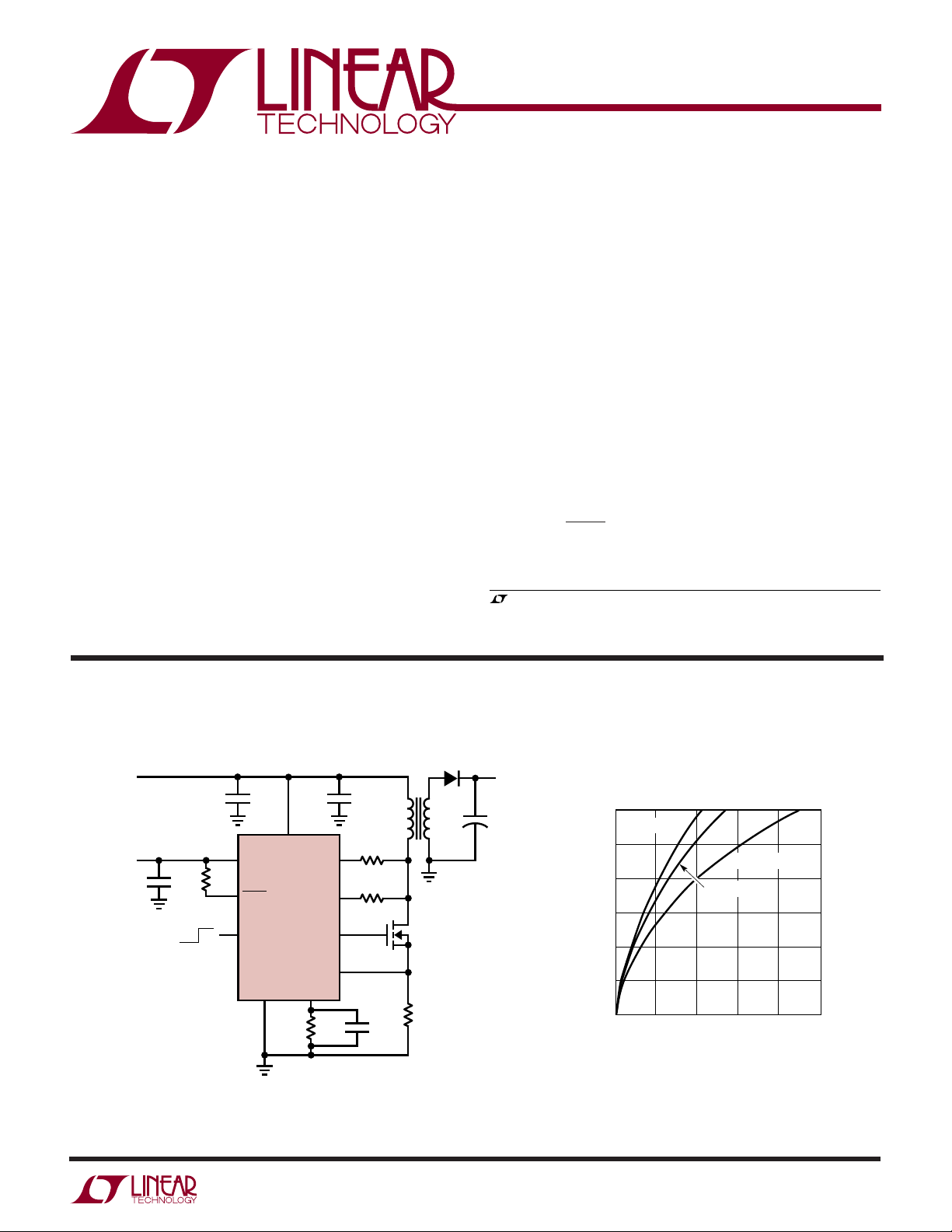
TYPICAL APPLICATIO
300V, 6A Capacitor Charger
V
TRANS
10µF
V
V
12V
CC
100k
10µF
OFF ON
TRANS
V
CC
DONE
LT3750
CHARGE
GND RBG
U
RV
OUT
RDCM
GATE
SOURCE
2.49k 100pF
56µF
×2
60.4k
43k
3750 TA01a
•
T1
1:10
M1
12mΩ
D1
•
V
OUT
300V
+
100µF
(V)
OUT
V
300
250
200
150
100
V
50
0
0
6A Charge Time
= 18V
TRANS
V
TRANS
0.1 0.2 0.3 0.4
TIME (SECONDS)
V
TRANS
= 12V
= 6V
0.5
3750 TA03c
3750fa
1
Page 2
LT3750
WWWU
ABSOLUTE AXI U RATI GS
PACKAGE/ORDER I FOR ATIO
UU
W
(Note 1)
VCC, V
RBG ....................................................................... 1.5V
SOURCE ................................................................... 1V
Current into RDCM Pin ........................................ ±1mA
Current into RV
, GATE, DONE, CHARGE ...................... 24V
TRANS
Pin ........................................ ±1mA
OUT
V
TRANS
DONE
CHARGE
V
GND
Current into DONE Pin ......................................... ±1mA
Operating Temperature Range (Note 2) .. – 40°C to 85°C
Storage Temperature Range ................ –65°C to 150°C
ELECTRICAL CHARACTERISTICS
temperature range, otherwise specifications are T
PARAMETER CONDITIONS MIN TYP MAX UNITS
Minimum V
Minimum V
VCC Quiescent Current Not Switching, CHARGE = 5V 1.6 2.5 mA
V
TRANS
CHARGE Pin Current CHARGE = 24V 24 µA
CHARGE Pin Enable Voltage
CHARGE Pin Disable Voltage
Minimum CHARGE Pin Low Time High→Low→High 20 µs
V
OUT
V
OUT
RBG Pin Bias Current RBG = 1.2V 70 500 nA
DCM Comparator Trip Voltage Measured as V
Current Limit Comparator Trip Voltage
DONE Output Signal High 100kΩ to 5V 4.9 5 V
DONE Output Signal Low 100kΩ to 5V 0.1 0.2 V
DONE Pin Leakage Current DONE = 2.5V 0.2 µA
NMOS Minimum On Time 0.6 µs
GATE Rise Time 50 ns
GATE High Voltage C
GATE Turn Off Propagation Delay C
CC
TRANS
Quiescent Current Not Switching, CHARGE = 5V 140 250 µA
Comparator Trip Voltage Measured RBG Pin
Comparator Overdrive 1µs Pulse Width, Measured on RBG Pin 30 mV
A
Not Switching, CHARGE = 0V 1 µA
Not Switching, CHARGE = 0V 1 µA
CHARGE = 5V 19 µA
CHARGE = 0V 1 µA
= 1nF, VCC = 5V 3 3.8 4.5 V
GATE
= 1nF, VCC = 24V 22 22.6 23.5 V
C
GATE
= 1nF 100 ns
GATE
The ● denotes specifications which apply over the full operating
= 25°C. VCC = V
– V
DRAIN
ORDER PART NUMBER MS PART MARKING
LT3750EMS
Order Options Tape and Reel: Add #TR
Lead Free: Add #PBF Lead Free Tape and Reel: Add #TRPBF
Lead Free Part Marking: http://www.linear.com/leadfree/
Consult LTC Marketing for parts specified with wider operating temperature ranges.
= 5V unless otherwise specified.
TRANS
, R
TRANS
= 43k (Note 3)
DCM
TOP VIEW
1
2
3
4
CC
5
MS PACKAGE
10-LEAD PLASTIC MSOP
T
= 125°C, θJA = 120°C/ W
JMAX
●
●
●
●
0.2 0.6 V
●
1.215 1.24 1.265 V
●
●
53680 mV
68 78 88 mV
10
RBG
9
RV
OUT
RDCM
8
GATE
7
SOURCE
6
LTBQD
2.8 3 V
2.5 3 V
0.87 1.1 V
Note 1: Stresses beyond those listed under Absolute Maximum Ratings
may cause permanent damage to the device. Exposure to any Absolute
Maximum Rating condition for extended periods may affect device
reliability and lifetime.
2
Note 2: The LT3750E is guaranteed to meet performance specifications
from 0°C to 70°C. Specifications over the –40°C to 85°C operating
temperature range are assured by design, characterization and correlation
with statistical process controls.
Note 3: Refer to Block Diagram for V
DRAIN
definition.
3750fa
Page 3
UW
V
CHARGE
(V)
0
0
CHARGE PIN CURRENT (µA)
5
15
20
25
16
45
3750 G03
10
8
4
20
12 24
30
35
40
–50°C
25°C
125°C
TEMPERATURE (°C)
–50 –25
0
GATE PIN VOLTAGE (V)
10
25
0
50
75
3750 G06
5
20
15
25
100
125
VCC = 24V
VCC = 12V
VCC = 5V
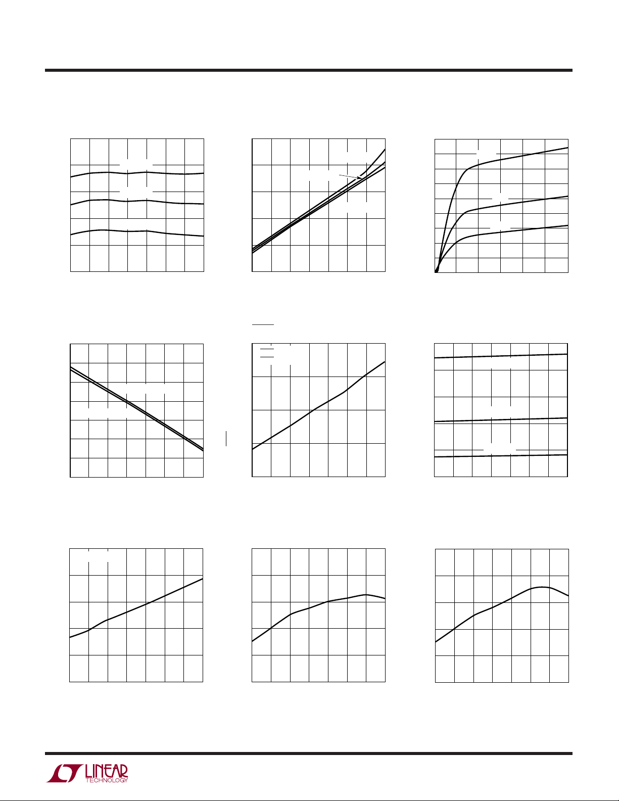
TYPICAL PERFOR A CE CHARACTERISTICS
LT3750
VCC Pin Current
1.8
1.7
1.6
1.5
PIN CURRENT (mA)
CC
V
1.4
1.3
–50 –25
VCC = 24V
VCC = 12V
VCC = 3V
25
0
TEMPERATURE (°C)
CHARGE Pin Enable/Disable
Voltage
0.9
0.8
0.7
0.6
CHARGE PIN DISABLE
0.5
CHARGE PIN ENABLE
V
Pin Current CHARGE Pin Current
TRANS
225
V
= 24V
200
V
TRANS
175
150
PIN CURRENT (µA)
TRANS
V
125
50
75
100
125
3750 G01
100
–50 –25
0
TEMPERATURE (°C)
DONE Output Signal Low
160
V
= 5V
DONE
= 100k
R
DONE
140
120
TRANS
= 12V
V
= 3V
TRANS
50
25
75
100
125
3750 G02
GATE High Voltage
0.4
CHARGE PIN VOLTAGE (V)
0.3
0.2
–50
60
50
40
30
20
DCM COMPARATOR TRIP VOLTAGE (mV)
10
–50 –25
50 100 125
–25 0
25 75
TEMPERATURE (°C)
DCM Comparator Trip Voltage
R
= 43k
DCM
50
25
0
TEMPERATURE (°C)
75
100
3750 G04
3750 G07
125
100
DONE PIN VOLTAGE (mV)
80
–50
–25 0 25 50
TEMPERATURE (°C)
V
Comparator Trip Voltage
OUT
1.240
1.236
1.232
1.228
COMPARATOR TRIP VOLTAGE (V)
1.224
OUT
V
1.220
–50 –25
25
0
TEMPERATURE (°C)
50
75 100 125
3750 G05
100
125
3750 G08
75
Current Limit Comparator Trip
Voltage
82
80
78
76
74
72
CURRENT LIMIT COMPARATOR TRIP VOLTAGE (mV)
–50 –25
0
TEMPERATURE (°C)
50
25
75
100
3750 G09
3750fa
3
125
Page 4

LT3750
U
UU
PI FU CTIO S
V
primary coil of the transformer as well as internal circuitry
that performs boundary mode detection. Bypass at the pin
with a 1µF to 10µF capacitor. Bypass the primary winding
of the transformer with a large capacitor.
DONE (Pin 2): Open Collector Indication Pin. When target
output voltage is reached, an NPN transistor turns on.
Requires a pull-up resistor or current source. Any fault
conditions such as thermal shutdown or undervoltage
lockout will also turn on the NPN.
CHARGE (Pin 3): Charge Pin. Initiates a new charge cycle
when brought high or discontinues charging and puts part
into shutdown when low. To properly enable the device, a
step input with a minimum ramp rate of 1V/µs is required.
Drive to 1.1V or higher to enable the device; drive below
0.2V to disable the device.
V
ceramic capacitor. A 1µF to 10µF ceramic capacitor should
be sufficient for most applications.
GND (Pin 5): Ground Pin. Connect directly to local ground
plane.
(Pin 1): Transformer Supply Pin. Powers the
TRANS
(Pin 4): Input Supply Pin. Bypass locally with a
CC
SOURCE (Pin 6): Source Pin. Senses NMOS drain current.
Connect NMOS source terminal and current sense resistor
to this pin. The current limit is 78mV/R
GATE (Pin 7): Gate Pin. Connect NMOS gate terminal to
this pin. Internal gate driver will drive voltage to within
VCC – 2V during each switching cycle.
RDCM (Pin 8): Discontinuous Mode Sense Pin. Senses
when current in transformer has decayed to zero and initiates a new charge cycle if output voltage target has not
been reached. Place a resistor between this pin and the drain
of the NMOS. A good choice is a 43k, 5% resistor.
RV
(Pin 9): Output Voltage VI Converter Pin. Develops
OUT
a current proportional to output capacitor voltage. Connect a resistor between this pin and the drain of the NMOS.
RBG (Pin 10): Output Voltage Sense Pin. Senses the
voltage across the RBG resistor, which is proportional to
the current flowing into the R
equals 1.24V, charging is disabled and DONE pin goes
low. Connect a resistor (2.5k or less is recommended)
from this pin to GND. A 2.49k, 1% resistor is a good
choice.
pin. When voltage
VOUT
SENSE
.
4
3750fa
Page 5
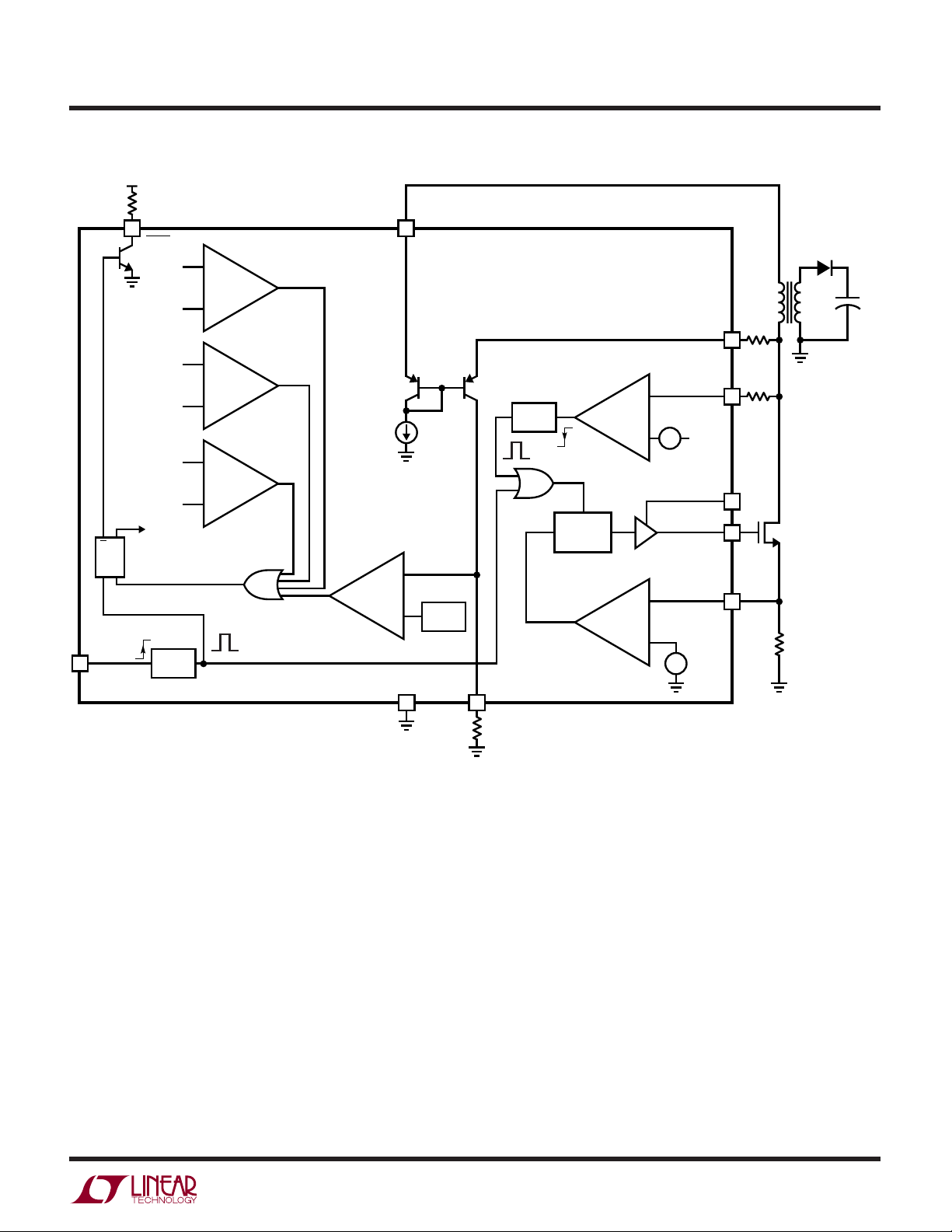
BLOCK DIAGRA
R
DONE
2
3
Q
RQS
CHARGE
DONE
2.8V
V
2.5V
V
TRANS
DIE
TEMP
160°C
M1
ENABLE
ONE
SHOT
CC
V
CC
UVLO
+
–
V
TRANS
UVLO
+
–
TSD
+
–
W
V
OUT
COMPARATOR
1
+
–
GND
5
V
TRANS
1.24V
LT3750
V
TRANS
D1
T1
1:N
•
R
RV
OUT
DCM
COMPARATOR
+
ONE
SHOT
–
S
QR
+
CURRENT LIMIT
COMPARATOR
RBG
10
R
BG
–
+
–
36mV
SOURCE
+
–
RDCM
V
TRANS
V
GATE
78mV
VOUT
9
R
DCM
8
V
CC
4
7
6
M1
R
3750 BD
DRAIN
SENSE
+
V
OUT
•
C
OUT
3750fa
5
Page 6

LT3750
OPERATIO
U
The LT3750 is designed to charge capacitors quickly and
efficiently. Operation can be best understood by referring
to Figures 1 and 2. Operation proceeds in four phases:
1. Start-up, 2. Primary-side charging, 3. Secondary energy transfer, 4. Discontinuous mode sensing.
1. Start-Up
Start-up occurs for approximately 20µs after the charge
pin is raised high. During this phase, a one-shot enables
the master latch and turns on the NMOS. The master latch
will remain in the set state until the target output voltage
is reached or a fault condition resets it.
I
LSEC
S2
+
•
V
SEC
–
3750 F01a
V
TRANS
I
LPRI
V
DRAIN
1:N
+
V
PRI
•
–
+
S1
–
2. Primary Side Charging
When the NMOS on latch is set, the gate driver rapidly
charges the gate pin to V
on forcing V
TRANS
– V
– 2V. The external NMOS turns
CC
across the primary winding.
DS(ON)
Consequently, current in the primary coil rises linearly at
I
LPRI
V
– V
TRANS
TRANS
DS(ON)
L
PRI
V
+ V
OUT
DIODE
L
SEC
– V
DS(ON)
I
I
LSEC
I
V
PK
PK
N
PRI
V
(1a) Equivalent Circuit During Primary-Side Charging
I
LSEC
S2
+
•
–
3750 F01b
V
TRANS
I
LPRI
V
DRAIN
+
+
V
•
–
1:N
PRIVSEC
S1
–
(1b) Equivalent Circuit During Secondary Energy
Transfer and Output Detection
I
LSEC
S2
+
•
V
SEC
–
3750 F01c
V
TRANS
I
V
LPRI
DRAIN
1:N
+
V
PRI
•
–
+
S1
–
(1c) Equivalent Circuit During Discontinuous Mode Detection
Figure 1. Equivalent Circuits
V
V
SEC
DRAIN
+
–(V
V
N
+ V
+
DIODE
DIODE
V
)
+ V
OUT
DIODE
N
DISCONTINUOUS
DETECTION
–N (V
TRANS
V
DS(ON)
1.
PRIMARY-SIDE
CHARGING
– V
)
DS(ON)
ENERGY TRANSFER
OUT
V
OUT
V
TRANS
2.
SECONDARY
AND OUTPUT
DETECTION
Figure 2. Idealized Charging Waveforms
3.
MODE
V
TRANS
V
DS(ON)
3750 F02
3750fa
6
Page 7

OPERATIO
LT3750
U
a rate (V
rored on the secondary winding –N • (V
TRANS
– V
DS(ON)
)/L
. The input voltage is mir-
PRI
TRANS
– V
DS(ON)
)
which reverse biases the diode and prevents current flow
in the secondary winding. Thus, energy is stored in the
core of the transformer.
3. Secondary Energy Transfer
When current limit is reached, the current limit comparator resets the NMOS on-latch and the device enters the
third phase of operation, secondary energy transfer. The
energy stored in the transformer core forward biases the
diode and current flows into the output capacitor. During
this time, the output voltage (neglecting the diode drop) is
reflected back to the primary coil. If the target output
voltage is reached, the V
comparator resets the master
OUT
latch and the DONE pin goes low. Otherwise, the device
enters the next phase of operation.
4. Discontinuous Mode Detection
Once all the current is transferred to the output capacitor,
(V
OUT
+ V
)/N will appear across the primary winding.
DIODE
A transformer with no energy cannot support a DC voltage,
so, the voltage across the primary will decay to zero. In
other words, the drain of the NMOS will ring down from
V
voltage falls to V
TRANS
+ (V
OUT
+ V
TRANS
DIODE
)/N to V
. When the drain
TRANS
+ 36mV, the DCM comparator sets
the NMOS on-latch and a new charge cycle begins. Steps
2-4 continue until the target output voltage is reached.
3750fa
7
Page 8

LT3750
WUUU
APPLICATIO S I FOR ATIO
Safety Warning
Large capacitors charged to high voltage can deliver a
lethal amount of energy if handled improperly. It is particularly important to observe appropriate safety measures when designing the LT3750 into applications. First,
create a discharge circuit that allows the designer to safely
discharge the output capacitor. Second, adequately space
high voltage nodes from adjacent traces to satisfy printed
circuit board voltage breakdown requirements. High voltage nodes are the drain of the NMOS, the secondary side
of the transformer, and the output.
Transformer Selection
The flyback transformer is critical to proper operation of
the LT3750. It must be designed carefully so that it does
not cause excessive current or voltage on any pin of the
part.
As with all circuits, the LT3750 has finite bandwidth. In
order to give the LT3750 sufficient time to detect the
output voltage, observe the following restrictions on the
primary inductance:
Switching Period
The LT3750 employs an open-loop control scheme causing the switching period to decrease with output voltage.
Typical switching frequency is between 100kHz to 300kHz.
Figure 3 shows typical switching period in an application
with a 3A peak current.
20
16
12
TIME (µs)
8
4
0
0
Figure 3. Typical Switching Period vs V
100 150 200
50
V
(V)
OUT
250 300
3750 F03
OUT
Output Diode Selection
When choosing the rectifying diode, ensure its peak
L
Vµs
OUT
≥
PRI
NI
••1
PK
repetitive forward current rating exceeds the peak cur-
otherwise, the LT3750 may overcharge the output.
Linear Technology has worked with several leading magnetic component manufacturers to produce flyback transformers for use with the LT3750. Table 1 summarizes the
particular transformer characteristics.
Table 1. Recommended Transformers
MANUFACTURER PART NUMBER SIZE L × W × H (mm) MAXIMUM I
TDK DCT15EFD-U44S003 22.5 × 16.5 × 8.5 5 10 1:10
(www.tdk.com) DCT20EFD-U32S003 30 × 22 × 12 10 10 1:10
Sumida C8118 Rev P1 21 × 14 × 8 3 10 1:10
(www.sumida.com) C8117 Rev P1 23 × 18.6 × 10.8 5 10 1:10
C8119 Rev P1 32.3 × 27 × 14 10 10 1:10
Midcom 32050 23.1 × 18 × 9.4 3 10 1:10
(www.midcom.com) 32051 28.7 × 22 × 11.4 5 10 1:10
32052 28.7 × 22 × 11.4 10 10 1:10
Coilcraft DA2032-AL 17.2 × 22 × 8.9 3 10 1:10
(www.coilcraft.com) DA2033-AL 17.4 × 24.1 × 10.2 5 10 1:10
DA2034-AL 20.6 × 30 × 11.3 10 10 1:10
rent (I
rating exceeds V
through the diode varies during the charge cycle because
the switching period decreases as V
average current through the diode is greatest when the
/N) and that the peak repetitive reverse voltage
PK
OUT
(A) L
PRI
+ (N)(V
(µH) TURNS RATIO (PRI:SEC)
PRI
). The average current
TRANS
increases. The
OUT
8
3750fa
Page 9

WUUU
APPLICATIO S I FOR ATIO
LT3750
output capacitor is almost completely charged and is
given by:
IV
•
I
AVG D
=
,
2
PK TRANS
VNV
()
OUT PK TRANS
()
•
+
The output diode’s continuous forward current rating
must exceed I
AVG,D
.
At a minimum, the diode must satisfy all the previously
mentioned specifications to guarantee proper operation.
However, to optimize charge time, reverse recovery time
and reverse bias leakage current should be considered.
Excessive diode reverse recovery times can cause appreciable discharging of the output capacitor thereby increasing charge time. Choose a diode with a reverse
recovery time of less than 100ns. Diode leakage current
under high reverse bias bleeds the output capacitor of
charge, also increasing charge time. Choose a diode that
has minimal reverse bias leakage current. Table 2 recommends several output diodes for various output voltages
with adequate reverse recovery time.
Table 2. Recommended Output Diodes
PEAK
REPETITIVE
REVERSE
PART I
MANUFACTURER NUMBER (A) (V) PACKAGE
Diodes Inc. MURS140 1 400 SMB
(www.diodes.com) MURS160 1 600 SMB
ES2G 2 400 SMB
US1M 1 1000 SMA
Philips BYD147 1 400 SOD87
(www.semiconductors. BYD167 1 500 SOD87
philips.com)
DC
VOLTAGE
Bypass Capacitor Selection
Use a high quality X5R or X7R dielectric ceramic capacitor
placed close to the LT3750 to locally bypass the VCC and
V
pins. For most applications, a 1µF to 10µF ceramic
TRANS
capacitor should suffice for VCC and a 1µF to 10µF for the
V
TRANS
pin.
can result in improper operation. This most often manifests itself in two ways. The first is when the primary winding current looks distorted instead of triangular. This
substantially reduces the efficiency and increases the
charge time. The second way is when the LT3750 fails to
detect discontinuous mode after the first switching cycle.
Both of these problems are solved by increasing the amount
of capacitive bypassing for the transformer. Choose capacitors that can handle the high RMS ripple currents
common in flyback regulators.
Output Capacitor Selection
For photoflash applications, the output capacitor will be
discharged into a Xenon flash bulb. Only a pulse capacitor
or photoflash capacitor is able to survive such a harsh
event. Igniting a typical Xenon bulb requires approximately 250V to 350V stored on a capacitor on the order of
hundreds of microfarads.
Table 3. Recommended Output Capacitor Vendors
VENDOR WEBSITE
Rubycon www.rubycon.com
Cornell Dubilier www.cornell-dubilier.com
NWL www.nwl.com
NMOS Selection
Choose an external NMOS with minimal gate charge and
on resistance that satisfies current limit and voltage breakdown requirements. The gate is nominally driven to VCC –
2V during each charge cycle. Ensure that this does not
exceed the maximum gate to source voltage rating of the
NMOS but enhaces the channel enough to minimize the on
resistance. Similarly, the maximum drain-source voltage
rating of the NMOS must exceed V
TRANS
+ V
/N or the
OUT
magnitude of the leakage inductance spike, whichever is
greater. The maximum instantaneous drain current must
exceed current limit. Because the switching period decreases with output voltage, the average current through
the NMOS is greatest when the output is nearly charged
and is given by:
The high peak currents flowing through the transformer
necessitate a larger (>>10µF) capacitor to bypass the pri-
mary winding of the transformer. Inadequate bypassing
I
AVG M
•
IV
=
,
PK OUT PK
2
VNV
()
()
OUT PK TRANS
+
()
•
3750fa
9
Page 10

LT3750
WUUU
APPLICATIO S I FOR ATIO
Table 4. Recommended NMOS Transisitors
MANUFACTURER PART NUMBER ID (A) V
Philips Semiconductor PHM21NQ15T 22.2 150 20 55 HVSON8
(www.semiconductors.philips.com) PHK12NQ10T 11.6 100 20 28 SO-8
PHT6NQ10Y 6.5 100 20 90 SOT223
PSMN038-100K 6.3 100 20 38 SO-8
International Rectifier IRF7488 6.3 80 20 29 SO-8
(www.irf.com) IRF7493 9.3 80 20 15 SO-8
IRF6644 10.3 100 20 10.7 DirectFET
DS(MAX)
(V) V
GS(MAX)
(V) R
(mΩ) PACKAGE
DS(ON)
The transistor’s continuous drain current rating must
exceed I
AVG,M
.
Table 4 lists recommended NMOS transistors.
Setting Current Limit
A sense resistor from the SOURCE pin to GND implements
current limit. The current limit is nominally 78mV/R
SENSE
.
The average power dissipation rating of the current sense
resistor must exceed:
P
RESISTOR
2
IR
•
PK SENSE
≥
3
⎛
⎜
⎝
V
OUT PK
()
+
VNV
OUT PK T
()
•
RRANS
⎞
⎟
⎠
Additionally, there is approximately a 100ns propagation
delay from the time that peak current limit is detected to
when the gate transitions to the low state. This delay
increases the peak current limit by (V
TRANS
)(t
DELAY
)/L
PRI
.
Setting The Target Output Voltage
The parameters that determine the target output voltage
are the resistors R
and RBG, the turns ratio of the
VOUT
transformer (N), and the voltage drop across the output
diode (V
). The target output voltage is set according
DIODE
to the following equation:
VV
⎛
=
OUT
124.• •–
⎜
⎝
R
VOUT
R
BG
⎞
NV
DIODE
⎟
⎠
Use at least 1% tolerance resistors for R
Choosing large value resistors for R
BG
and RBG.
VOUT
decreases the
amount of current that charges the parasitic internal
capacitances and degrades the response time of the V
OUT
comparator. This may result in overcharging of the output
capacitor. The maximum recommended value for R
BG
is
2.5k for typical applications.
When high primary currents are used, a voltage spike
can prematurely trip the output voltage comparator. A
33pF to 100pF capacitor in parallel with R
is sufficient to
BG
filter this spike for most applications. Always check that
the voltage waveform on RBG does not overshoot and that
it reaches a plateau at maximum V
OUT
.
Discontinuous Mode Detection
The R
resistor stands off voltage transients on the
DCM
drain node. A 43k, 5% resistor is recommended for 300V
applications. Higher output voltages will require a larger
resistor.
In order for the LT3750 to properly detect discontinuous
mode and start a new charge cycle, the reflected voltage to
the primary winding must exceed the discontinuous mode
comparator threshold which is nominally 36mV. The
worst-case condition occurs when V
is shorted to
OUT
ground. When this occurs, the reflected voltage is simply
the diode forward voltage drop divided by N.
10
3750fa
Page 11

WUUU
APPLICATIO S I FOR ATIO
LT3750
Board Layout
The high voltage operation of the the LT3750 demands
careful attention to board layout. Observe the following
points:
1. Minimize the area of the high voltage end of the secondary winding.
2. Provide sufficient spacing for all high voltage nodes
(NMOS drain, V
and the secondary winding of the
OUT
transformer) in order to meet breakdown voltage
requirements.
C
V
TRANS
R
DONE
CHARGE
V
TRANS
1
2
3
CC
4
5
C
IN
LT3750
R
R
SENSE
BG
10
9
8
7
6
3. Keep the electrical path formed by C1, the primary of T1
and drain of the NMOS as small as possible. Increasing
the size of this path effectively increases the leakage
inductance of T1 resulting in an overvoltage condition
on the drain of the NMOS.
D
C
PRI
R
DCMRVOUT
T1
1:N
PRIMARY
•
OUT
•
SECONDARY
+
C
OUT
M1
Figure 4. Recommended Board Layout
(Not to Scale)
3750 F04
3750fa
11
Page 12

LT3750
TYPICAL APPLICATIO S
V
TRANS
V
CC
12V
U
300V, 3A Capacitor Charger
C2
10µF
V
TRANS
V
C1
10µF
OFF ON
C1: 25V X5R OR X7R CERAMIC CAPACITOR
C2: 25V X5R OR X7R CERAMIC CAPACITOR
C3: 25V SANYO OS-CON 25SVP56M
C4: 330V RUBYCON PHOTOFLASH CAPACITOR
D1: DIODES INC. MURS160
M1: PHILIPS PHT6NQ10T
T1: TDK DCT15EFD-U44S003 FLYBACK TRANSFORMER
CC
100k
DONE
CHARGE
GND RBG
RV
RDCM
LT3750
SOURCE
C3
56µF
60.4k
OUT
43k
GATE
2.49k 33pF
1:10
4, 5
•
6, 7110
3750 TA02a
T1
M1
25mΩ
D1
•
V
OUT
300V
+
C4
100µF
100
90
80
70
EFFICIENCY (%)
60
50
0
3A Charging Efficiency 3A Charge Time
300
V
= 18V
(V)
OUT
V
250
200
150
100
TRANS
V
TRANS
V
= 12V
TRANS
50
0
0
0.2 0.4 0.6 0.8
TIME (SECONDS)
TRANS
100 150 200
50
V
TRANS
= 12V
V
OUT
(V)
= 18V
V
TRANS
= 6VV
250 300
3750 TA02b
= 6V
3750 TA02c
1.0
NMOS DRAIN
CURRENT
1A/DIV
NMOS DRAIN
VOLTAGE
20V/DIV
Typical Switching Waveforms
5µs/DIV
3750 TA02d
12
3750fa
Page 13

U
TYPICAL APPLICATIO S
V
TRANS
V
CC
12V
300V, 6A Capacitor Charger
C2
10µF
V
TRANS
V
C1
10µF
OFF ON
C1: 25V X5R OR X7R CERAMIC CAPACITOR
C2: 25V X5R OR X7R CERAMIC CAPACITOR
C3: 25V SANYO OS-CON 25SVP56M
C4: 330V RUBYCON PHOTOFLASH CAPACITOR
D1: DIODES INC. MURS160
M1: PHILIPS PHT6NQ10T
T1: TDK DCT20EFD-U32S003 FLYBACK TRANSFORMER
CC
100k
DONE
CHARGE
GND RBG
RV
RDCM
LT3750
SOURCE
C3
56µF
×2
60.4k
OUT
43k
GATE
2.49k 100pF
T1
1:10
3, 4, 5, 6
•
7, 8, 9, 10112
M1
12mΩ
3750 TA03a
LT3750
D1
•
V
OUT
300V
+
C4
100µF
100
90
80
70
EFFICIENCY (%)
60
50
0
6A Charging Efficiency 6A Charge Time
300
V
= 18V
TRANS
(V)
OUT
V
250
200
150
100
V
TRANS
V
= 12V
TRANS
50
0
0
0.1 0.2 0.3 0.4
TIME (SECONDS)
100 150 200
50
V
TRANS
V
TRANS
V
TRANS
V
OUT
= 18V
= 12V
= 6V
250 300
(V)
3750 TA03b
= 6V
3750 TA03c
0.5
NMOS DRAIN
CURRENT
2A/DIV
NMOS DRAIN
VOLTAGE
20V/DIV
Typical Switching Waveforms
5µs/DIV
3750 TA03d
3750fa
13
Page 14

LT3750
TYPICAL APPLICATIO S
V
TRANS
V
CC
12V
U
C1
10µF
OFF ON
300V, 9A Capacitor Charger
C2
10µF
V
TRANS
V
CC
100k
DONE
CHARGE
GND RBG
LT3750
RV
OUT
RDCM
GATE
SOURCE
2.49k 100pF
C3
56µF
×3
60.4k
43k
3, 4, 5, 6
7, 8, 9, 10
3750 TA04a
T1
D1
1:10
1
•
•
12
M1
8mΩ
V
OUT
300V
+
C4
100µF
100
90
80
EFFICIENCY (%)
70
60
0
C1: 25V X5R OR X7R CERAMIC CAPACITOR
C2: 25V X5R OR X7R CERAMIC CAPACITOR
C3: 25V SANYO OS-CON 25SVP56M
C4: 330V RUBYCON PHOTOFLASH CAPACITOR
D1: DIODES INC. MURS160
M1: PHILIPS PHM2INQ15T
T1: TDK DCT20EFD-U32S003 FLYBACK TRANSFORMER
9A Charging Efficiency 9A Charge Time
300
V
= 18V
TRANS
(V)
OUT
V
250
200
150
100
50
0
0
0.05 0.10 0.15 0.20
V
V
TRANS
TIME (SECONDS)
TRANS
100 150 200
50
V
TRANS
V
TRANS
V
TRANS
V
OUT
= 18V
= 12V
= 6V
250 300
(V)
3750 TA04b
= 12V
= 6V
3750 TA04c
0.300.25
NMOS DRAIN
CURRENT
4A/DIV
NMOS DRAIN
VOLTAGE
20V/DIV
Typical Switching Waveforms
5µs/DIV
3750 TA04d
14
3750fa
Page 15

PACKAGE DESCRIPTIO
U
MS Package
10-Lead Plastic MSOP
(Reference LTC DWG # 05-08-1661)
0.889 ± 0.127
(.035 ± .005)
LT3750
5.23
(.206)
MIN
0.305 ± 0.038
(.0120 ± .0015)
TYP
RECOMMENDED SOLDER PAD LAYOUT
0.254
(.010)
GAUGE PLANE
0.18
(.007)
NOTE:
1. DIMENSIONS IN MILLIMETER/(INCH)
2. DRAWING NOT TO SCALE
3. DIMENSION DOES NOT INCLUDE MOLD FLASH, PROTRUSIONS OR GATE BURRS.
MOLD FLASH, PROTRUSIONS OR GATE BURRS SHALL NOT EXCEED 0.152mm (.006") PER SIDE
4. DIMENSION DOES NOT INCLUDE INTERLEAD FLASH OR PROTRUSIONS.
INTERLEAD FLASH OR PROTRUSIONS SHALL NOT EXCEED 0.152mm (.006") PER SIDE
5. LEAD COPLANARITY (BOTTOM OF LEADS AFTER FORMING) SHALL BE 0.102mm (.004") MAX
3.20 – 3.45
(.126 – .136)
DETAIL “A”
DETAIL “A”
0.50
(.0197)
BSC
° – 6° TYP
0
0.53 ± 0.152
(.021 ± .006)
SEATING
PLANE
3.00 ± 0.102
(.118 ± .004)
(NOTE 3)
4.90 ± 0.152
(.193 ± .006)
0.17 – 0.27
(.007 – .011)
TYP
1.10
(.043)
MAX
12
0.50
(.0197)
BSC
8910
3
7
6
45
0.497 ± 0.076
(.0196 ± .003)
REF
3.00 ± 0.102
(.118 ± .004)
(NOTE 4)
0.86
(.034)
REF
0.127 ± 0.076
(.005 ± .003)
MSOP (MS) 0603
Information furnished by Linear Technology Corporation is believed to be accurate and reliable.
However, no responsibility is assumed for its use. Linear Technology Corporation makes no representation that the interconnection of its circuits as described herein will not infringe on existing patent rights.
3750fa
15
Page 16

LT3750
TYPICAL APPLICATIO
V
TRANS
V
12V
U
300V, 9A, 2.5mF Capacitor Charger
T1
D1
1:10
C3
60.4k
43k
56µF
×3
3750 TA05a
4, 5
•
6, 7110
M1
8mΩ
•
C2
10µF
V
CC
C1
100k
10µF
OFF ON
TRANS
V
CC
DONE
CHARGE
GND RBG
RV
RDCM
LT3750
GATE
SOURCE
OUT
2.49k 100pF
V
OUT
300V
+
C4
2.5mF
C1, C2: 25V X5R OR X7R CERAMIC CAPACITOR
C3: 25V SANYO OS-CON 25SVP56M
C4: CORNELL DUBILIER 7P252V360N082
D1: DIODES INC. MURS160
M1: PHILIPS PHM21NQ15T
T1: MIDCOM 32052 FLYBACK TRANSFORMER
Efficiency Charge Time
100
95
90
85
EFFICIENCY (%)
80
75
70
0
100 150 200
50
V
TRANS
V
TRANS
V
TRANS
V
OUT
= 18V
= 12V
= 6V
250 300
(V)
3750 TA05b
(V)
OUT
V
300
V
= 18V
TRANS
250
200
150
100
50
0
0
123456
TIME (SECONDS)
V
TRANS
= 6V
V
TRANS
= 12V
87
3750 TA05c
RELATED PARTS
PART NUMBER DESCRIPTION COMMENTS
LT3420/LT3420-1 1.4A/1A, Photoflash Capacitor Charger with Charges 220µF to 320V in 3.7 Seconds from 5V, VIN: 2.2V to 16V,
Automatic Top-Off I
LT3468/LT3468-1 1.4A, 1A, 0.7A, Photoflash Capacitor Charger VIN: 2.5V to 16V, Charge Time: 4.6 Seconds for LT3468 (0V to 320V, 100µF,
LT3468-2 V
LT3484-0/LT3484-1 1.4A, 0.7A, 1A Photoflash Capacitor Charger VIN: 1.8V to 16V, Charge Time: 4.6 Seconds for LT3484-0
LT3484-2 (0V to 320V, 100µF, V
LT3485-0/LT3485-1 1.4A, 0.7A, 1A, 2A Photoflash Capacitor Charger VIN: 1.8V to 10V, Charge Time: 3.7 Seconds for LT3485-0
LT3485-2/LT3485-3 with Output Voltage Monitor and Integrated IGBT (0V to 320V, 100µF, V
< 1µA, 10-Lead MS Package
SD
= 3.6V), ISD < 1µA, ThinSOT Package
IN
= 3.6V), ISD < 1µA, 2mm × 3mm 6-Lead
IN
DFN Package
= 3.6V), ISD < 1µA, 3mm × 3mm 10-Lead DFN
IN
Driver
16
Linear Technology Corporation
1630 McCarthy Blvd., Milpitas, CA 95035-7417
(408) 432-1900 ● FAX: (408) 434-0507
●
www.linear.com
3750fa
LT 0106 REV A • PRINTED IN THE USA
© LINEAR TECHNOLOGY CORPORATION 2005
 Loading...