

Page 1

LT3742
Dual, 2-Phase Step-Down
Switching Controller
FEATURES
■
Wide Input Voltage Range: 4V to 30V
■
Wide Output Voltage Range: 0.8V to V
■
Low Shutdown IQ: 20μA
■
Out-of-Phase Controllers Reduce Required Input
IN
Capacitance and Power Supply Induced Noise
■
0.8V ±1.5% Voltage Reference
■
500kHz Current Mode Fixed Frequency Operation
■
Internal Boost Converter Provides Bias Rail for
N-Channel MOSFET Gate Drive
■
Power Good Voltage Monitor for Each Output
■
Programmable Soft-Start
■
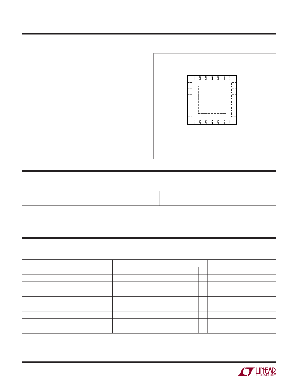
24-Lead 4mm × 4mm × 0.75mm Package
APPLICATIONS
■
Satellite and Cable TV Set-Top Boxes
■
Distributed Power Regulation
■
Automotive Systems
■
Super Capacitor Charger
DESCRIPTION
The LT®3742 is a dual step-down DC/DC switching regulator
controller that drives high side N-channel power MOSFETs.
A 500kHz fi xed frequency current mode architecture provides fast transient response with simple loop compensation components and cycle-by-cycle current limiting. The
output stages of the two controllers operate 180° out of
phase to reduce the input ripple current, minimizing the
noise induced on the input supply, and allowing less input
capacitance.
An internal boost regulator generates a bias rail of V
to provide gate drive for the N-channel MOSFETs allowing
low dropout and 100% duty cycle operation. The LT3742
can be used for applications where both controllers need
to operate independently, or where both controllers are
used to provide a single higher current output.
The device is available in a thermally enhanced 4mm ×
4mm QFN package.
, LT, LTC and LTM are registered trademarks of Linear Technology Corporation.
All other trademarks are the property of their respective owners.
IN
+ 7V
TYPICAL APPLICATION
8V and 5V Dual Step-Down Converter
V
IN
V
OUT1
RUN1
8V
4A
47μF
14V
V
IN
10μF
0.010Ω
1.8k
200Ω
1000pF
1nF
6.5μH
1μF
PG1
30k
45.3k
20.0k
V
UVLO
G1
SW1
SENSE1
SENSE1
FB1
PG1
RUN/SS1
V
10μH
SWB
IN
LT3742
+
SENSE2
–
SENSE2
C1
RUN/SS2
GND
BIAS
SW2
FB2
PG2
V
μF
4.7
Effi ciency vs Load Current
100
90
V
IN
1.05k
200Ω
1nF
10μF
47μF
3742 TA03a
V
OUT2
5V
4A
RUN2
G2
6.5μH
0.010Ω
+
–
PG2
C2
20k
1000pF
80
70
EFFICIENCY (%)
60
50
40
0.5 1.5
0
12
LOAD CURRENT (A)
8V
OUT
5V
OUT
3
2.5
3.5
3742 TA03b
4
3742f
1
Page 2
LT3742
ABSOLUTE MAXIMUM RATINGS
(Note 1)
VIN Voltage ................................................................30V
UVLO Voltage ............................................................30V
PG1, PG2 Voltage .....................................................30V
SWB, BIAS Voltage ...................................................40V
+
SENSE1
SENSE1
, SENSE2+ Voltage ......................................30V
–
, SENSE2– Voltage ......................................30V
RUN/SS1, RUN/SS2 Voltage .......................................6V
FB1, FB2 Voltage .........................................................6V
, VC2 Voltage ..........................................................6V
V
C1
Junction Temperature ........................................... 125°C
Operating Junction Temperature Range
(Note 2) .................................................. –40°C to 125°C
Storage Temperature Range ................... –65°C to 125°C
ORDER INFORMATION
PIN CONFIGURATION
TOP VIEW
SW1NCNC
24 23 22 21 20 19
1
V
2
IN
UVLO
3
BIAS
4
SWB
5
6
G2
7 8 9
SW2
24-LEAD (4mm × 4mm) PLASTIC QFN
T
EXPOSED PAD (PIN 25) IS GND, MUST BE SOLDERED TO PCB
JMAX
SENSE1+SENSE1–FB1
25
10 11 12
+
NC
–
SENSE2
SENSE2
NC
UF PACKAGE
= 125°C, θJA = 36°C/W
FB2
18G1
17
16
15
14
13
V
C1
PG1
RUN/SS1
RUN/SS2
PG2
V
C2
LEAD FREE FINISH TAPE AND REEL PART MARKING PACKAGE DESCRIPTION TEMPERATURE RANGE
LT3742EUF#PBF LT3742EUF#TRPBF 3742 24-Lead (4mm × 4mm) Plastic QFN –40°C to 125°C (Note 2)
Consult LTC Marketing for parts specifi ed with wider operating temperature ranges.
Consult LTC Marketing for information on non-standard lead based fi nish parts.
For more information on lead free part marking, go to: http://www.linear.com/leadfree/
For more information on tape and reel specifi cations, go to: http://www.linear.com/tapeandreel/
ELECTRICAL CHARACTERISTICS
The ● denotes the specifi cations which apply over the full operating
temperature range, otherwise specifi cations are at TA = 25°C. VIN = 5V unless otherwise specifi ed.
PARAMETER CONDITIONS MIN TYP MAX UNITS
Minimum Operating Input Voltage V
Quiescent Current V
Shutdown Current V
= 1.5V
UVLO
RUN/SS1
RUN/SS1
= V
= V
= V
= V
RUN/SS2
RUN/SS2
FB1
= 0V 20 35 μA
= 1V 5.0 7.0 mA
FB2
UVLO Pin Threshold UVLO Pin Voltage Rising
UVLO Pin Hysteresis Current V
= 1V, Current Flows Into Pin 1.8 2.7 4 μA
UVLO
RUN/SS Pin Threshold 0.2 0.6 V
RUN/SS Pin Charge Current V
= 0V 0.5 0.9 1.5 μA
RUN/SS
FB Pin Voltage
FB Pin Voltage Line Regulation V
= 5V to 30V 0.01 %/V
IN
●
●
1.20 1.24 1.28 V
●
0.788 0.800 0.812 V
3.5 4.0 V
2
3742f
Page 3

LT3742
ELECTRICAL CHARACTERISTICS
The ● denotes the specifi cations which apply over the full operating
temperature range, otherwise specifi cations are at T
PARAMETER CONDITIONS MIN TYP MAX UNITS
FB Pin Bias Current V
FB Pin Voltage Matching –4 0 4 mV
Error Amplifi er Transconductance 250 μmho
Error Amplifi er Voltage Gain 500 V/V
Pin Source Current VFB = 0.6V 15 μA
V
C
Pin Sink Current VFB = 1V 15 μA
V
C
Controller Switching Frequency 440 500 560 kHz
Switching Phase 180 Deg
Maximum Current Sense Voltage V
Current Sense Matching Between Controllers ±5 %
Current SENSE Pins Total Current SENSE
Gate Rise Time C
Gate Fall Time C
Gate On Voltage (V
Gate Off Voltage (V
PG Pin Voltage Low I
Lower PG Trip Level (Relative to V
Lower PG Trip Level (Relative to V
Upper PG Trip Level (Relative to V
Upper PG Trip Level (Relative to V
PG Pin Leakage Current V
PG Pin Sink Current V
Bias Pin Voltage V
SWB Pin Current Limit 250 340 500 mA
SWB Pin Leakage Current V
Bias Supply Switching Frequency 0.88 1.0 1.12 MHz
– VSW)V
G
– VSW)V
G
)V
FB
)V
FB
)V
FB
)V
FB
= 25°C. VIN = 5V unless otherwise specifi ed.
A
= 0.8V, VC = 0.4V 50 200 nA
FB
–
= 3.3V
SENSE
–
, SENSE+ = 0V
–
SENSE
, SENSE+ = 3.3V
= 3300pF 40 ns
LOAD
= 3300pF 60 ns
LOAD
= 5V, V
IN
= 5V, V
IN
= 100μA 0.20 0.5 V
PG
Increasing –7 –10 –13 %
FB
Decreasing –10 –13 –16 %
FB
Increasing 7 10 13 %
FB
Decreasing 4 7 10 %
FB
= 2V, VFB = 1V 0.1 μA
PG
= 0.5V 200 500 μA
PG
= 12V 0.01 1 μA
SWB
= 12V 6.0 6.7 7.0 V
BIAS
= 12V 0.4 0.75 V
BIAS
●
50 60 70 mV
–1.0
40
+ 6.6 VIN + 7 VIN + 7.7 V
IN
mA
μA
Note 1: Stresses beyond those listed under Absolute Maximum Ratings
may cause permanent damage to the device. Exposure to any Absolute
Maximum Rating condition for extended periods may affect device
reliability and lifetime.
Note 2: The LT3742E is guaranteed to meet performance specifi cations
from 0°C to 125°C operating junction temperature range. Specifi cations
over the –40°C to 125°C operating junction temperature range are
assured by design, characterization and correlation with statistical process
controls.
3742f
3
Page 4
LT3742
TYPICAL PERFORMANCE CHARACTERISTICS
IQ-SHDN vs Temperature IQ-Running vs Temperature
50
40
10
9
8
Controller Current Sense Voltage
vs Temperature
70
65
30
CURRENT (μA)
20
10
–50
–25 0 25 50
TEMPERATURE (°C)
75 100 125
3742 G01
7
6
CURRENT (mA)
5
4
3
–50
–25 0
50 100 125
25 75
TEMPERATURE (°C)
3742 G02
VIN Minimum vs Temperature UVLO Threshold vs Temperature V
3.0
2.5
2.0
1.5
UVLO (V)
1.0
0.5
0
–50
–25 0
50 100 125
25 75
TEMPERATURE (°C)
3742 G05
(V)
IN
V
5
4
3
2
1
–50
–25 0 25 50
TEMPERATURE (°C)
75 100 125
3742 G04
60
SENSE VOLTAGE (mV)
55
50
–50
–25 0 25 50
vs Temperature
FB
830
820
810
(mV)
800
FB
V
790
780
770
–50
–25 0
TEMPERATURE (°C)
50 100 125
25 75
TEMPERATURE (°C)
75 100 125
3742 G03
3742 G06
4
RUN/SS Current vs Temperature UVLO I
1.8
1.2
(μA)
HYST
I
0.6
RUN/SS CURRENT (μA)
0
–25–50
0 255075
TEMPERATURE (°C)
100 125
3742 G07
3.0
2.8
2.6
2.4
2.2
2.0
–50 –25
vs Temperature
HYST
25
0
TEMPERATURE (°C)
50
75
100
125
3742 G08
3742f
Page 5
TYPICAL PERFORMANCE CHARACTERISTICS
Controller Frequency vs
Temperature
600
PG Threshold vs Temperature V
1.0
LT3742
– V
BIAS
10
vs Temperature
IN
550
500
FREQUENCY (kHz)
450
400
–50
–25 0 25 50
TEMPERATURE (°C)
75 100 125
SWB Current Limit vs
Temperature
380
360
340
320
SWB CURRENT LIMIT (mA)
3742 G09
0.9
0.8
0.7
FEEDBACK VOLTS RISING (V)
0.6
–50
–25 0 25 50
POWER GOOD
TEMPERATURE (°C)
75 100 125
3742 G10
RUN/SS Threshold vs
Temperature
1.0
0.7
0.4
RUN/SS VOLTS (V)
8
) (V)
IN
– V
BIAS
(V
6
4
–50 –25 0 25 50
TEMPERATURE (°C)
75 100 125
3742 G11
300
–50
–25 0 25 50
TEMPERATURE (°C)
75 100 125
3742 G12
0.1
–25
0255075
TEMPERATURE (°C)
100 125
3742 G13
3742f
5
Page 6

LT3742
PIN FUNCTIONS
G1, G2 (Pins 1, 6): Gate Drives. These pins provide high
current gate drive for the external N-channel MOSFETs.
These pins are the outputs of fl oating drivers whose voltage swings between the BIAS and SW pins.
(Pin 2): Input Voltage. This pin supplies current to the
V
IN
internal circuitry of the LT3742. This pin must be locally
bypassed with a capacitor.
UVLO (Pin 3): Undervoltage Lockout. Do not leave this
pin open ; connect it to V
connected to V
input voltage at which the LT3742 will operate. When this
pin is less than 1.25V, the controllers are disabled (the
RUN/SS pins are still used to turn on each switching
regulator). Once this pin drops below 1.25V, a 3μA current
sink draws current into the pin to provide programmable
hysteresis for UVLO.
BIAS (Pin 4): Bias for Gate Drive. This pin provides a bias
voltage higher than the input voltage to drive the external
N-channel MOSFETs. The voltage on this pin is regulated
+ 7V.
to V
IN
SWB (Pin 5): Bias Regulator Switch. This is the collector of an internal NPN switch used to generate the bias
voltage to provide gate drive for the external N-channel
MOSFETs.
is tied to this pin to program the minimum
IN
if not used. A resistor divider
IN
PG1, PG2 (Pins 17, 14): Power Good. These pins are
open-collector outputs of internal comparators. PG remains
low until the FB pin is within 90% of the fi nal regulation
voltage. As well as indicating output regulation, the PG
pins can be used to sequence the switching regulators.
The PG outputs are valid when V
and either of the RUN/SS pins is high. The power good
comparators are disabled in shutdown. If not used, these
pins should be left unconnected.
, VC2 (Pins 18, 13): Control Voltage and Compensation
V
C1
Pins for Internal Error Amplifi ers. Connect a series RC
from these pins to ground to compensate each switching
regulator loop.
FB1, FB2 (Pins 19, 12): Feedback Pins. The LT3742
regulates these pins to 800mV. Connect the feedback
resistors to this pin to set the output voltage for each
switching regulator.
–
SENSE1
Sense Inputs. These pins (along with the SENSE
are used to sense the inductor current for each switching
regulator.
SENSE1
Inputs. These pins (along with the SENSE
sense the inductor current for each switching regulator.
, SENSE2– (Pins 20, 11): Negative Current
+
, SENSE2+ (Pins 21, 10): Positive Current Sense
is greater than 3.5V
IN
+
pins)
–
pins) are used to
RUN/SS1, RUN/SS2 (Pins 16, 15): Run/Soft-Start Pins.
These pins are used to shut down each controller. They
also provide a soft-start function with the addition of an
external capacitor. To shut down any regulator, pull the
RUN/SS pin to ground with an open-drain or open-collector device. If neither feature is used, leave these pins
unconnected.
SW1, SW2 (Pins 24, 7): Switch Nodes. These pins connect
to the source of the external N-channel MOSFETs and to
the external inductors and diodes.
Exposed Pad (Pin 25): Ground. The Exposed Pad of the
package provides both electrical contact to ground and
good thermal contact to the printed circuit board. The
Exposed Pad must be soldered to the circuit board to
ensure proper operation.
3742f
6
Page 7
BLOCK DIAGRAM
LT3742
SHDN
SWB
5
BIAS
SENSE
SENSE
SW
4
G
+
–
FB
V
C
GND
25
V
IN
2
3
V
IN
UVLO
RUN/SS
1.25V
LT3742 CONTROLLER 1 AND 2
COMPARATOR
3μA
TO ENABLE
1μA
UNDERVOLTAGE
+
–
UVLO
≈0.5V
TO
RUN/SS1
RUN/SS2
LOCKOUT
ENABLE
COMPARATOR
–
+
+
PWM
COMPARATOR
SS
ENABLE
R
Q
S
GATE DRIVE BIAS
BOOST REGULATOR
THERMAL
SHUTDOWN
PHASE SYNC
500kHz SLAVE
OSCILLATOR
Σ
+
–
V
REF
INTERNAL
SUPPLY
1MHz MASTER
OSCILLATOR
CURRENT
SENSE
AMPLIFIER
ERROR
AMPLIFIER
1.25V
0.86V
0.80V
0.74V
DC/DC CONTROLLERS
BIAS
GATE
DRIVER
+
–
–
+
0.80V
+
BIAS
ENABLE
QDQ
PHASE SYNC FOR
V
IN
V
IN
V
OUT
PGOOD
–
PG
POWER GOOD
COMPARATORS
0.86V
+
FB
–
+
0.74V
3742 BD1
3742f
7
Page 8

LT3742
OPERATION
The LT3742 is a dual, constant frequency, current mode
DC/DC step-down controller. The two controllers in each
device share some common circuitry including protection circuitry, the internal bias supply, voltage reference,
master oscillator and the gate drive boost regulator. The
Block Diagram shows the shared common circuitry and
the independent circuitry for both DC/DC controllers.
Important protection features included in the LT3742 are
undervoltage lockout and thermal shutdown. When either
of these conditions exist, the gate drive bias regulator and
both DC/DC controllers are disabled and both RUN/SS pins
are discharged to ~0.7V to get ready for a new soft-start
cycle. Undervoltage lockout (UVLO) is programmed using
two external resistors. When the UVLO pin drops below
1.25V, a 3μA current sink is activated to provide programmable hysteresis for the UVLO function. A separate, less
accurate, internal undervoltage lockout will disable the
LT3742 when V
The gate drive boost regulator is enabled when all internal
fault conditions have been cleared. This regulator uses
both an internal NPN power switch and Schottky diode to
generate a voltage at the BIAS pin that is 7V higher than
the input voltage. Both DC/DC controllers are disabled until
the BIAS voltage has reached ~90% of its fi nal regulation
voltage. This ensures that suffi cient gate drive to fully
enhance the external MOSFETs is present before the driver
is allowed to turn on.
The master oscillator runs at 1MHz and clocks the gate
drive boost regulator at this frequency. The master oscillator also generates two 500kHz clocks, 180° out of phase,
for the DC/DC controllers.
is less than 3V.
IN
A power good comparator pulls the PG pin low whenever
the FB pin is not within ±7.5% of the 800mV internal
reference voltage. PG is the open-collector output of an
NPN that is off when the FB pin is in regulation, allowing
an external resistor to pull the PG pin high. This power
good indication is valid only when the device is enabled
(RUN/SS is high) and V
The LT3742 enables each controller independently when its
RUN/SS pin is above ~0.5V and each controller generates
its own soft-start ramp. During start-up, the error amplifi er
compares the FB pin to the soft-start ramp instead of the
precision 800mV reference, which slowly raises the output
voltage until it reaches its resistor programmed regulation
point. Control of the inductor current is strictly maintained
until the output voltage is reached. The LT3742 is ideal
for applications where both DC/DC controllers need to
operate separately.
A pulse from the 500kHz oscillator sets the RS fl ip-fl op
and turns on the external N-channel MOSFET. Current in
the switch and the external inductor begins to increase.
When this current reaches a level determined by the control
voltage (V
turning off the MOSFET. The current in the inductor then
fl ows through the external Schottky diode and begins to
decrease. This cycle begins again at the next set pulse from
the slave oscillator. In this way, the voltage at the V
controls the current through the inductor to the output.
The internal error amplifi er regulates the output voltage
by continually adjusting the V
of the peak inductor current on a cycle-by-cycle basis is
managed by the current sense amplifi er. Because the inductor current is constantly monitored, the devices inherently
provide excellent output short-circuit protection.
), the PWM comparator resets the fl ip-fl op,
C
is 4V or greater.
IN
pin voltage. Direct control
C
pin
C
8
3742f
Page 9

APPLICATIONS INFORMATION
LT3742
Soft-Start and Shutdown
The RUN/SS (Run/Soft-Start) pins are used to enable each
controller independently, and to provide a user-programmable soft-start function that reduces the peak input
current and prevents output voltage overshoot during
start-up. To disable either controller, pull its RUN/SS pin
to ground with an open-drain or open-collector device.
If both RUN/SS pins are pulled to ground, the LT3742 is
placed in shutdown mode, and quiescent current is reduced to ~20μA. Internal 1μA current sources pull up on
each RUN/SS pin, and when either pin reaches ~0.5V, that
controller is enabled, along with the internal bias supply,
gate drive boost regulator, voltage reference and master
oscillator. If both outputs are always enabled together,
one soft-start capacitor can be used with both RUN/SS
pins tied together.
The Benefi ts of Soft-Start
When a capacitor is tied from the RUN/SS pin to ground,
the internal 1μA pull-up current source generates a voltage ramp on this pin. During start-up, the error amplifi er
compares the FB pin to this ramp instead of to the 800mV
reference; this slowly and smoothly increases the output
voltage to its fi nal value, while maintaining control of the
inductor current. Always check the inductor current and
output voltage waveforms to ensure that the programmed
soft-start time is long enough. A new soft-start cycle will
be initiated whenever V
drops low enough to trigger
IN
undervoltage lockout (programmed using the UVLO pin),
or the LT3742 die temperature exceeds thermal shutdown.
A typical value for the soft-start capacitor is 1nF.
Soft-start is strongly recommended for all LT3742 applications, as it provides the least amount of stress on
the external power MOSFET and catch diode. Without
soft-start, both of these components will see the maximum current limit every start-up cycle. Figures 1a and 1b
show start-up waveforms with and without soft-start for
the circuit of Figure 1. Notice the large inductor current
spike and the output voltage overshoot when soft-start is
not used. While this may be acceptable for some systems,
the addition of a single capacitor dramatically improves
the start-up behavior of each DC/DC controller.
V
OUT
5V/DIV
I
L
2A/DIV
0.5ms/DIV
Figure 1a. Start-Up Waveforms Without Soft-Start Figure 1b. Start-Up Waveforms with 1nF Soft-Start Capacitor
3742 F01a
V
OUT
5V/DIV
2A/DIV
I
L
0.5ms/DIV
3742 F01b
3742f
9
Page 10

LT3742
APPLICATIONS INFORMATION
Power Good Indicators
The PG pin is the open-collector output of an internal
window comparator that is pulled low whenever the FB
pin is not within ±7.5% of the 800mV internal reference
voltage. Tie the PG pin to any supply less than 30V with
a pull-up resistor that will supply less than 200μA. This
pin will be open when the LT3742 is placed in shutdown
mode regardless of the voltage at the FB pin. The power
good indication is valid only when the LT3742 is enabled
(RUN/SS is high) and V
SHDN
Figure 2a. Supply Sequencing with Controller 2 Delayed Until After Controller 1 is in Regulation
is 3V or greater.
IN
4.7nF
4.7nF
LT3742
RUN/SS1
PG1
RUN/SS2
SHDN (REFERENCE)
Output Sequencing and Tracking
The RUN/SS and PG pins can be used together to sequence
the two outputs of the LT3742. Figure 3 shows three
circuits to do this. For the fi rst two cases, controller 1
starts fi rst.
In Figure 2a, controller 2 turns on only after controller
1 has reached within 10% of its fi nal regulation voltage.
A larger value for the soft-start capacitor on RUN/SS2
will provide additional delay between the outputs. One
V
OUT1
5V/DIV
V
OUT2
10V/DIV
5ms/DIV
3742 F02a
LT3742
SHDN
RUN/SS1
4.7nF
RUN/SS2
10nF
SHDN (REFERENCE)
V
OUT1
5V/DIV
V
OUT2
10V/DIV
5ms/DIV
Figure 2b. Supply Sequencing with Controller 2 Having a Fixed Delay Relative to Controller 1
LT3742
SHDN
RUN/SS1
10nF
RUN/SS2
SHDN (REFERENCE)
V
OUT1
5V/DIV
V
OUT2
10V/DIV
5ms/DIV
Figure 2c. Both Conditions Start Up Together with Ratiometic Tracking
3742 F02b
3742 F02c
3742f
10
Page 11

APPLICATIONS INFORMATION
LT3742
characteristic to notice about this method is that if the
output of controller 1 goes out of regulation enough
to trip the power good comparator, controller 2 will be
disabled.
In Figure 2b, a slightly larger capacitor on RUN/SS2 delays
the turn-on of controller 2 with respect to controller 1. The
start-up waveforms for this method look very similar to
the one shown in Figure 6a, but here controller 2 is not
disabled if controller 1 goes out of regulation.
In Figure 2c, both RUN/SS pins share a single capacitor
and start up at the same time. By sharing the same softstart signal, this method provides ratiometric tracking of
the two outputs.
Undervoltage Lockout (UVLO)
An external resistor divider can be used to accurately
set the minimum input voltage at which the LT3742 will
operate. Figure 3 shows the basic UVLO operation. Once
the UVLO pin drops below 1.25V, an undervoltage lockout event is signaled, turning on a 3μA current source to
provide hysteresis.
During a UVLO event, both controllers and the gate drive
boost regulator are disabled. For the LT3742, all RUN/SS
pins are discharged to get ready for a new soft-start cycle.
For each controller that is enabled, it’s RUNSS pin will be
held to ~700mV until the input voltage rises above the
upper UVLO trip voltage. The UVLO function is only active
when one or more of the controllers are enabled using the
RUN/SS pin. The UVLO pin can not be used to directly
start the part. Do not leave the UVLO pin unconnected;
tie it to V
undervoltage lockout will disable the LT3742 when V
if not used. A separate, less accurate, internal
IN
is
IN
less than 3.5V.
The UVLO resistor values are chosen to give the desired
minimum operating voltage (V
amount of hysteresis (V
). The LT3742 will turn on
HYST
when the input voltage is above (V
once on, will turn off when V
the value for R
V
=
R
UV
1
27
RR
UV UV
21
fi rst, then select the value for R
UV1
HYST
μ=.
A
•
V
()
IN MIN
drops below V
IN
125
.
V
125
–.
) and the desired
IN(MIN)
+ V
IN(MIN)
IN(MIN)
VV
HYST
), and
. Select
.
UV2
Input Voltage Range
The minimum input voltage is determined by either the
LT3742’s minimum operating voltage of 4V, UVLO or by
the output voltages of a given application. The LT3742 can
operate at 100% duty cycle, so if the input voltage drops
close to or equal to one of the output voltages, the controller will go into low dropout operation (100% duty cycle).
The duty cycle is the fraction of the time the N-channel
MOSFET is on every switch cycle, and is determined by
the input and output voltages:
⎛
VV
+
DC
=
OUT D
⎜
⎝
VV V
–
IN DS D
⎞
⎟
⎠
+
where VD is the forward drop of the catch diode (~0.4V)
and V
is the typical MOSFET voltage drop (~0.1V).
DS
V
V
IN
R
UV1
R
UV2
IN
2
1.25V
UVLO
3
Figure 3. Undervoltage Lockout
+
–
3μA
UVLO
3742 F03
3742f
11
Page 12

LT3742
APPLICATIONS INFORMATION
The maximum input voltage is determined by the absolute
maximum ratings of the V
spectively) and by the minimum duty cycle, DC
⎛
VV
OUT D
⎜
⎝
DC
V
IN MAX
and BIAS pins (30V and 40V, re-
IN
⎞
+
MIN
VV
+
⎟
SW D()
⎠
–=
MIN
= 15%.
The formula above calculates the maximum input voltage
that allows the part to regulate without pulse-skipping,
and is mainly a concern for applications with output voltages lower than 3.3V. For example, for a 2.5V output, the
maximum input voltage is:
V
IN MAX()
⎛
25 04
..
+
VV
⎜
015
⎝
.
⎞
+=
01 04 19
.–.=
⎟
⎠
VVV
If an input voltage higher than ~19V is used, the 2.5V output
will still regulate correctly, but the part must pulse-skip
to do so. Pulse skipping does not damage the LT3742,
but it will result in erratic inductor current waveforms
and higher peak currents. Note that this is a restriction
on the operating input voltage only for a specifi c output
voltage; the circuit will tolerate inputs up to the absolute
maximum rating.
The Benefi ts of 2-Phase Operation
Traditionally, dual controllers operate with a single phase.
This means that both power MOSFETs are turned on at
the same time, causing current pulses of up to twice the
amplitude of those from a single regulator to be drawn
from the input capacitor. These large amplitude pulses
increase the RMS current fl owing in the input capacitor,
require the use of larger and more expensive input capacitors, increase EMI, and causes increased power losses in
the input capacitor and input power supply.
The two controllers of the LT3742 are guaranteed by design
to operate 180° out of phase. This assures that the current
in each power MOSFET will never overlap, always presenting a signifi cantly low peak and RMS current demand to
the input capacitor. This allows the use of a smaller, less
expensive input capacitor, improving EMI performance
and real world operating effi ciency.
Figure 4 shows example waveforms for a single phase dual
controller versus a 2-phase LT3742 system. In this case,
5V and 3.3V outputs, each drawing a load current of 2A,
are derived from a 12V supply. In this example, 2-phase
Single Phase
Dual Controller
SW1 (V)
SW2 (V)
I
L1
I
L2
I
IN
Figure 4. Example Waveforms for a Single Phase Dual Controller vs the 2-Phase LT3742
2-Phase
Dual Controller
3742 F04
3742f
12
Page 13

APPLICATIONS INFORMATION
LT3742
operation would reduce the RMS input capacitor current
from ~1.8A
RMS
to ~0.8A
. While this is an impressive
RMS
reduction by itself, remember that power losses are pro-
2
portional to I
, meaning that the actual power wasted
RMS
due to the input capacitor is reduced by a factor of ~4.
Figure 5 shows the reduction in RMS ripple current for a
typical application.
The reduced input ripple current also means that less
power is lost in the input power path. Improvements in
both conducted and radiated EMI also directly accrue as
a result of the reduced RMS input current and voltage.
Signifi cant cost and board footprint savings are also realized by being able to use smaller, less expensive, lower
RMS current-rated input capacitors.
Of course, the improvement afforded by 2-phase operation is a function of the relative duty cycles of the two
controllers, which in turn, are dependent upon the input
voltage (DC ≈ V
OUT/VIN
).
It can be readily seen that the advantages of 2-phase operation are not limited to a narrow operating range, but in
fact extend over a wide region. A good rule of thumb for
most applications is that 2-phase operation will reduce the
input capacitor requirement to that for just one channel
operating at maximum current and 50% duty cycle.
Inductor Value Selection
The inductor value directly affects inductor ripple current,
I
RIPPLE
, and maximum output current, I
OUT(MAX)
. Lower
ripple current reduces core losses in the inductor, ESR
losses in the output capacitors and output voltage ripple.
Too large of a value, however, will result in a physically
large inductor. A good tradeoff is to choose the inductor
ripple current to be ~30% of the maximum output current.
This will provide a good tradeoff between the inductor
size, maximum output current, and the amount of ripple
current. Note that the largest ripple current occurs at the
highest the input voltage, so applications with a wide V
range should consider both V
IN(TYP)
and V
IN(MAX)
IN
when
calculating the inductor value:
VVIV
≥
03
IN OUT
.•
OUT MAX
()
L
OUT
••
V kHz
IN
–
1
500
This equation provides a good starting point for picking the inductor value. Most systems can easily tolerate
ripple currents in the range of 10% to 50%, so deviating
slightly from the calculated value is acceptable for most
applications. Pick a standard value inductor close to the
3.0
SINGLE PHASE
2.5
2.0
1.5
1.0
INPUT RMS CURRENT (A)
0.5
VO1 = 5V/3A
= 3.3V/3A
V
O2
0
0
Figure 5. RMS Input Current Comparison
DUAL CONTROLLER
2-PHASE
DUAL CONTROLLER
10 20 30 40
INPUT VOLTAGE (V)
3742 F05
3742f
13
Page 14

LT3742
APPLICATIONS INFORMATION
value calculated above, and then recheck the amount of
ripple current:
VVLV
I
RIPPLE
–
IN OUT OUT
=
••
V kHz
IN
1
500
The DC resistance (DCR) of the inductor can have a
signifi cant impact on total system effi ciency, as it causes
2
R
an I
power loss. Consider inductance value, DCR,
DCR
and current rating when choosing an inductor. Table 1
shows several recommended inductor vendors. Each offers numerous devices in a wide variety of values, current
ratings, and package sizes.
Table 1. Recommended Inductor Manufacturers
VENDOR WEBSITE
Sumida www.sumida.com
Toko www.toko.com
Würth www.we-online.com
NEC-Tokin www.nec-tokinamerica.com
TDK www.tdk.com
Maximum Output Current (R
Value Selection)
SENSE
Maximum output current is determined largely by the
values of the current sense resistor, RSENSE (which sets
the inductor peak current), and the inductor (which sets
the inductor ripple current). The LT3742 current comparator has a guaranteed minimum threshold of 50mV, which
does not vary with duty cycle. The maximum output current is calculated:
–=
I
RIPPLE
2
I
OUT MAX
()
50
R
SENSE
mV
Rearranging the equation above to solve for RSENSE
gives:
mV
R
SENSE
=
I
OUT MAX
50
+
()
I
⎛
RIPPLE
⎜
⎝
⎞
⎟
⎠
2
Inductor, Catch Diode and MOSFET Current Rating
Once the inductor and R
values have been chosen, the
SENSE
current ratings of the inductor, catch diode and MOSFET
can then be determined. The LT3742 current comparator
has a guaranteed maximum threshold of 70mV, and there
is a small amount of current overshoot resulting from
the response time of the current sense comparator. The
components should be rated to handle:
I
RATED
70
mV
≥+
R
SENSE
V
⎛
IN
⎜
⎝
L
⎞
100•
ns
⎟
⎠
Schottky Catch Diode Selection
During output short-circuits, the diode will conduct current
most of the time, so it is important to choose a device
with a suffi cient current rating. In addition, the diode must
have a reverse voltage rating greater than the maximum
input voltage. Many surface mount Schottky diodes are
available in very small packages. Read their data sheets
carefully as they typically must be temperature derated.
Basically, excessive heating prevents them from being
used effectively at their rated maximum current. A few
recommended diodes are listed in Table 2.
Table 2. Recommended Schottky Diodes
VENDOR DEVICE
Diodes, Inc.
www.diodes.com
Microsemi
www.microsemi.com
On Semiconductor
www.onsemi.com
PDS540 (5A, 40V)
SBM1040 (10A, 40V)
UPS340 (3A, 40V)
UPS840 (8A, 40V)
MBRD320 (3A, 20V)
MBRD340 (3A, 40V)
Power MOSFET Selection
There are several important parameters to consider when
choosing an N-channel power MOSFET: drain current
(maximum I
); threshold voltage (V
V
GS
reverse transfer capacitance (C
); breakdown voltage (maximum VDS and
D
); on-resistance (R
GS(TH)
); and total gate charge
RSS
DS(ON)
);
14
3742f
Page 15

APPLICATIONS INFORMATION
LT3742
(QG). A few simple guidelines will make the selection
process easier.
The maximum drain current must be higher than the
maximum rated current, I
page. Note that the I
dependent (lower I
specifi cation is largely temperature
D
at higher ambient temperatures), so
D
most data sheets provide a graph or table of I
, calculated on the previous
RATED
versus
D
temperature to show this.
Ensure that the V
the maximum input voltage and that the V
breakdown voltage is greater than
DS
breakdown
GS
voltage is 8V or greater. The peak-to-peak gate drive
for each MOSFET is ~7V, so also ensure that the device
chosen will be fully enhanced with a V
preclude the use of some MOSFETs with a 20V V
of 7V. This may
GS
rating,
GS
as some have too high of a threshold voltage. A good rule
of thumb is that the maximum threshold voltage should be
V
GS(TH)(MAX)
≤ 3V. 4.5V MOSFETs will work as well.
Power losses in the N-channel MOSFET come from two
main sources: the on-resistance, R
transfer capacitance, C
2
ohmic losses (I
R
DS(ON)
. The on-resistance causes
RSS
) which typically dominate at
, and the reverse
DS(ON)
input voltages below ~15V. The reverse transfer capacitance results in transition losses which typically dominate
for input voltages above ~15V. At higher input voltages,
transition losses rapidly increase to the point that the use
of a higher R
device with lower C
DS(ON)
will actually
RSS
provide higher effi ciency. The power loss in the MOSFET
can be approximated by:
P ohmic loss transition loss
=
LOSS
P
LOSS
()
⎛
V
OU
≈
TTD
⎜
VV
+
⎝
IN D
VI
••
2
()
IN O
V
+
2
+
()
2
IR
OUT DS ON T
Cf••
UUT RSS
()
⎞
ρ
⎟
⎠
+••
where f is the switching frequency (500kHz) and ρT is a
normalizing term to account for the on-resistance change
due to temperature. For a maximum ambient temperature
of 70°C, using ρ
The tradeoff in R
≈ 1.3 is a reasonable choice.
T
DS(ON)
and C
can easily be seen in an
RSS
example using real MOSFET values. To generate a 3.3V,
3A (10W) output, consider two typical N-channel power
MOSFETs, both rated at V
= 30V and both available in
DS
the same SO-8 package, but having ~5x differences in
on-resistance and reverse transfer capacitance:
= 11.5A, VGS = 12V, R
M1: I
D
= 6.5A, VGS = 20V, R
M2: I
D
DS(ON)
DS(ON)
= 10mΩ, C
= 50mΩ, C
RSS
RSS
= 230pF
= 45pF
Power loss is calculated for both devices over a wide input
voltage range (4V ≤ V
≤ 30V), and shown in Figure 6 (as
IN
a percentage of the 10W total power). Note that while the
low R
device power loss is 5× lower at low input
DS(ON)
0.7
0.6
0.5
0.4
0.3
0.2
MOSFET POWER LOSS (W)
0.1
0
0
Figure 6a. Power Loss Example for M1 (10mΩ, 230pF)
OHMIC + TRANSITION
510
INPUT VOLTAGE (V)
TOTAL =
TRANSITION
OHMIC
20 30
15 25
3742 F06a
0.7
0.6
0.5
0.4
0.3
0.2
MOSFET POWER LOSS (W)
0.1
0
0
510
Figure 6b. Power Loss Example for M2 (50mΩ, 45pF)
TOTAL =
OHMIC + TRANSITION
OHMIC
TRANSITION
INPUT VOLTAGE (V)
20 30
15 25
3742 F06b
15
3742f
Page 16

LT3742
APPLICATIONS INFORMATION
voltages, it is also 3× higher at high input voltages when
compared to the low C
Total gate charge, Q
gate charge corresponds to a small value of C
device.
RSS
, is closely related to C
G
RSS
RSS
. Low
. Many
manufacturers have MOSFETs advertised as “low gate
charge” devices (which means they are low C
devices)
RSS
that are specifi cally designed for low transition loss, and
are ideal for high input voltage applications.
Input Capacitor Selection
For most applications, 10μF to 22μF of input capacitance
per channel will be suffi cient. A small 1μF bypass capacitor
between the V
and ground pins of the LT3742, placed
IN
close to the device, is also suggested for optimal noise
immunity. Step-down regulators draw current from the
input supply in pulses with very fast rise and fall times.
The input capacitor is required to reduce the resulting
voltage ripple at the LT3742 and to force this very high
frequency switching current into a tight local loop, minimizing EMI. The input capacitor must have low impedance at
the switching frequency to do this effectively, and it must
have an adequate ripple current rating. With two controllers operating at the same frequency but with different
phases and duty cycles, calculating the input capacitor
RMS current is not simple. However, a conservative value
is the RMS input current for the channel that is delivering
• I
the most power (V
I
I
RMS CIN
I
RMS(CIN)
OUT
V
IN
is largest (I
OUT
••–=
OUT
):
OUT
VVV
()
OUT IN OUT()
/2) when VIN = 2V
(at DC =
OUT
50%). As the second, lower power channel draws input
current, the input capacitor’s RMS current actually decreases as the out-of-phase current cancels the current
drawn by the higher power channel, so choosing an input
capacitor with an RMS ripple current rating of I
OUT,MAX
/2
is suffi cient.
The combination of small size and low impedance (low
equivalent series resistance, or ESR) of ceramic capacitors
make them the preferred choice. The low ESR results in
very low input voltage ripple and the capacitors can handle
plenty of RMS current. They are also comparatively robust
and can be used at their rated voltage. Use only X5R or
X7R types because they retain their capacitance over wider
voltage and temperature ranges than other ceramics.
An alternative to a high value ceramic capacitor is a lower
value (1μF) along with a larger value (10μF to 22μF) electrolytic or tantalum capacitor. Because the input capacitor
is likely to see high surge currents when the input source
is applied, tantalum capacitors should always be surge
rated. The manufacturer may also recommend operation
below the rated voltage of the capacitor. Be sure to place
the 1μF ceramic as close as possible to the N-channel
power MOSFET.
Output Capacitor Selection
A good starting value for output capacitance is to provide
10μF of C
for every 1A of output current. For lower
OUT
output voltages (under 3.3V) and for applications needing
the best possible transient performance, the ratio should
be 20μF to 30μF of C
for every 1A of output current.
OUT
X5R and X7R ceramics are an excellent choice for the
output capacitance. Aluminum electrolytics can be used,
but typically the ESR is too large to deliver low output
voltage ripple. Tantalum and newer, lower ESR organic
electrolytic capacitors are also possible choices, and the
manufactures will specify the ESR. Because the volume of
the capacitor determines the ESR, both the size and value
will be larger than a ceramic capacitor that would give you
similar output ripple voltage performance.
The output capacitor fi lters the inductor ripple current to
generate an output with low ripple. It also stores energy
in order to satisfy transient loads and to stabilize the
16
3742f
Page 17

APPLICATIONS INFORMATION
LT3742
LT3742’s control loop. Output ripple can be estimated
with the following equation:
VI
RIPPLE L
⎛
=Δ +
⎜
⎝
1
fC
8• •
SW OUT
ESR
⎞
⎟
⎠
where ΔIL is the inductor ripple current and fSW is the
switching frequency (500kHz). The ESR is so low for ceramic capacitors that it can be left out of the above calculation. The output voltage ripple will be highest at maximum
input voltage (ΔI
increases with input voltage). Table 3
L
shows several low-ESR capacitor manufacturers.
Table 3. Low ESR Surface Mount Capacitors
VENDOR TYPE SERIES
Taiyo Yuden
www.t-yuden.com
Murata
www.murata.com
Kemet
www.kemet.com
Sanyo
www.sanyo.com
Panasonic
www.panasonic.com
TDK
www.tdk.com
Nippon Chemicon
www.chemi-con.co.jp
Ceramic X5R, X7R
Ceramic X5R, X7R
Tantalum
Ta Organic
Al Organic
Ta or Al Organic POSCAP
Al Organic SP CAP
Ceramic X5R, X7R
Ceramic X5R, X7R
T491, T494, T495
T520
A700
Setting Output Voltage
The output of a bipolar controller requires a minimum load
to prevent current sourced from the switch pin charging
the output capacitor above the desired output voltage.
This current, approximately 5mA, may be accounted for
in the feedback string or the user may choose to force a
minimum load in their application.
The output voltage for each controller is programmed
with a resistor divider between the output and the FB pin.
Always use 1% resistors (or better) for the best output
voltage accuracy. The value of R
should be 8k or less,
A
and the value of R1 should be chosen according to:
RR
BA
⎛
=
OUT
•
⎜
⎝
.–08
⎞
1
⎟
⎠
V
V
Output Short-Circuit Protection
Because the LT3742 constantly monitors the inductor
current, both devices inherently providing excellent output
short-circuit protection. The N-channel MOSFET is not allowed to turn on unless the inductor current is below the
threshold of the current sense comparator. This guarantees that the inductor current will not “run away” and the
controller will skip cycles until the inductor current has
dropped below the current sense threshold.
Loop Compensation
An external resistor and capacitor connected in series from
pin to ground provides loop compensation for each
the V
C
controller. Sometimes a second, smaller valued capacitor
is placed in parallel to fi lter switching frequency noise from
pin. Loop compensation determines the stability
the V
C
and transient performance of each controller.
A practical approach is to start with values of R
and C
= 330pF, then tune the compensation network to
C
= 10k
C
optimize the performance. When adjusting these values,
change only one value at a time (R
or CC), then see how
C
the transient response is affected. The simplest way to
check loop stability is to apply a load current step while
observing the transient response at the output. Stability
should then be checked across all operating conditions,
including load current, input voltage, and temperature to
ensure a robust design.
V
OUT1
LT3742
R1B
V
FB1
R1A
Figure 7. Setting Output Voltage with the FB Pin
V
FB2
3742 F07
V
OUT2
R2B
R2A
3742f
17
Page 18

LT3742
APPLICATIONS INFORMATION
Bias Supply Considerations
The LT3742 uses an internal boost regulator to provide a
bias rail for enhancement of the external MOSFETs. This
bias rail is regulated to V
+ 7V and must be in regula-
IN
tion before either controller is allowed to start switching.
As this is a high speed switching regulator, standard
procedures must be followed regarding placement of the
external components. The SWB node should be kept small
to reduce EMI effects and the bias decoupling capacitor
) should be kept close to the BIAS pin and VIN. A
(C
BIAS
slight surplus of power is available from this supply and
it can be tapped after stringent engineering evaluation.
PC Board Layout Considerations
As with all switching regulators, careful attention must be
paid to the PCB board layout and component placement.
■
Place the power components close together with short
and wide interconnecting traces. The power components consist of the top MOSFETs, catch diodes and
the inductors C
and C
IN
. One way to approach this
OUT
is to simply place them on the board fi rst.
■
Similar attention should be paid to the power compo-
nents that make up the boost converter. They should also
be placed close together with short and wide traces.
■
Always use a ground plane under the switching regulator
to minimize interplane coupling.
■
Minimize the parasitic inductance in the loop of CIN,
MOSFET and catch diode, which carry large switching
currents.
■
Use compact plane for switch node (SW) to improve
cooling of the MOSFETs and to keep EMI low.
■
Use planes for VIN and V
to maintain good voltage
OUT
fi ltering and to keep power losses low. Unused areas
can be fi lled with copper and connect to any DC node
, V
(V
IN
■
Place CB close to BIAS pin and input capacitor.
■
Keep the high dv/dt nodes (SW1, SW2, G1, G2, C
C
IN2
, GND).
OUT
IN1
, SWB) away from sensitive small-signal nodes.
,
Demo board gerber fi les are available to assist with a
reliable layout. It will be diffi cult to achieve data sheet
performance specifi cations with improper layout.
18
3742f
Page 19

APPLICATIONS INFORMATION
V
IN
V
IN
SYSTEM
GROUND
V
OUT1
LT3742
RUN1
SHDN
RUN2
SHDN
V
IN
VIAS TO LOCAL GROUND PLANE
OUTLINE OF LOCAL GROUND PLANE
Figure 8. A Good PCB Layout Ensures Proper, Low EMI Operation
V
OUT2
3742 F08
3742f
19
Page 20

LT3742
TYPICAL APPLICATIONS
Supercap Charger Plus a DC/DC Buck Converter
V
OUT1
PG1
5V
4A
V
5.5V TO 30V
V
RUN1
IN
IN
C2
150μF
C5
1μF
C1
6.8μF
R
S1
4.7μH
0.010Ω
R1
1.05k
R2
200Ω
M3
C7
1nF
C
C1
680pF
D1, D2: DIODES INC. PDS1040
M1, M2: SILICONIX Si7884DP
L1
357k
124k
D1
R7
R8
M1
R
51k
L3
μH
22
254
V
SWB
IN
3
UVLO
LT3742
1
G1
24
SW1
21
20
19
17
16
18
C1
SENSE1
SENSE1
FB1
PG1
RUN/SS1
V
C1
+
–
GND
25
BIAS
SW2
SENSE2
SENSE2
FB2
PG2
RUN/SS2
V
C6
μF
4.7
V
3742 TA02
IN
SUPERCAP
CHARGER
OUTPUT
150mF
RUN2
PG2
6
G2
+
–
C2
M2
L2
7
10
11
12
14
15
13
47μH
D2
C8
1nF
C
C2
1000pF
R
S2
0.030Ω
6.8μF
47μF
M4
C3
C4
V
OUT1
PG1
8V and 5V Dual Step-Down Converter
L3
μH
V
IN
14V
1μF
V
IN
C1
10μF
R
S1
8V
4A
C2
47μF
RUN1
0.01Ω
R1
1.8k
R2
200Ω
M3
C2, C4: MURATA GRM32ER71A476K
D1, D2: DIODES INC. PDS1040
L1, L2: WÜRTH ELEKTRONIK 744314650
M1, M2: FAIRCHILD FDS4470
C5
C7
1nF
1000pF
C
L1
6.5μH
C1
45.3k
20k
D1
R1
R1
M1
R
30k
24
21
20
19
17
16
18
C1
22
254
V
SWB
IN
3
UVLO
LT3742
1
G1
SW1
+
SENSE1
–
SENSE1
FB1
PG1
RUN/SS1
V
C1
GND
25
BIAS
SW2
SENSE2
SENSE2
FB2
PG2
RUN/SS2
V
C6
μF
2.2
V
6
G2
+
–
C2
M2
L2
R
20k
6.5μH
D2
C8
C2
1nF
C
C2
1000pF
7
10
11
12
14
15
13
R
S2
0.01Ω
10μF
1.05k
200Ω
M4
C3
IN
V
OUT2
5V
R3
C4
47μF
R4
RUN2
3742 TA05
4A
PG2
3742f
20
Page 21

TYPICAL APPLICATIONS
V
IN
14V
V
IN
10μF 10μF
V
OUT1
3.3V
220μF
4A
10mΩ 10mΩ
619Ω
200Ω
5V and 3.3V Dual Step-Down Converter
L3
μH
1μF
L1
3.3μH
348k
130k
V
IN
UVLO
G1
SW1
SENSE1
SENSE1
FB1
22
SWB
LT3742
+
–
BIAS
SW2
SENSE2
SENSE2
2.2
G2
+
–
FB2
LT3742
μF
V
IN
L2
4.7μH
D2
1.05k
200Ω
V
5V
4A
150μF
OUT2
PG1
PG1
RUN/SS1
1nF 1nF
680pF 68pF
51k
D1, D2: DIODES INC. PDS1040
L1: VISHAY IHLP2525CZER3R3
L2: VISHAY IHLP2525CZER4R7
L3: COILCRAFT: ME3220-223KL
M1, M2: VISHAY Si7848DP-T1-E3
V
C1
GND
PG2
RUN/SS2
V
PG2
C2
51k
680pF
Effi ciency vs Load Current
90
5V
OUT
3.3V
80
70
EFFICIENCY (%)
60
50
0
1
LOAD CURRENT (A)
OUT
2
3
4
3742 TA01b
3742 TA01
3742f
21
Page 22

LT3742
TYPICAL APPLICATIONS
High Current, Low Ripple 12V Step-Down Converter
V
IN
24V
V
IN
V
OUT1
12V
8A
C
OUTA-COUTD
D1, D2: DIODES INC. PDS1040
L1, L2: NEC/TOKIN PLC12458R2
M1, M2: ROHM RSS065N03
: KEMET T495E107K020E060
C1
10μF
R1
2.8k
R2
200Ω
R
S1
0.010Ω
C7
1nF
C
680pF
8.2μH
C1
L1
C5
1μF
D1
M1
R7
124k
R8
20.0k
R
C1
51k
C
OUTA
100μF
20V
PG1
L3 10μH
V
IN
UVLO
G1
SW1
SENSE1
SENSE1
PG1
FB1
RUN/SS1
V
C1
C
OUTB
100μF
20V
SWB
LT3742
+
–
GND
BIAS
SW2
SENSE2
SENSE2
FB2
PG2
RUN/SS2
V
C
OUTC
100μF
20V
C6
4.7
μF
V
IN
R
S2
0.010Ω
C3
10μF
3742 TA04a
PG2
C
100μF
20V
M2
L2
8.2μH
D2
OUTD
G2
+
–
C2
22
12V
OUT
100
90
85
EFFICIENCY (%)
70
60
0
1234
Effi ciency vs Load Currnt
5678
LOAD CURRENT (A)
3742 TA04b
3742f
Page 23

PACKAGE DESCRIPTION
LT3742
UF Package
24-Lead Plastic QFN (4mm × 4mm)
(Reference LTC DWG # 05-08-1697)
0.70 ±0.05
4.50 ± 0.05
3.10 ± 0.05
2.45 ± 0.05
(4 SIDES)
RECOMMENDED SOLDER PAD PITCH AND DIMENSIONS
4.00 ± 0.10
(4 SIDES)
PIN 1
TOP MARK
(NOTE 6)
NOTE:
1. DRAWING PROPOSED TO BE MADE A JEDEC PACKAGE OUTLINE MO-220 VARIATION (WGGD-X)—TO BE APPROVED
2. DRAWING NOT TO SCALE
3. ALL DIMENSIONS ARE IN MILLIMETERS
4. DIMENSIONS OF EXPOSED PAD ON BOTTOM OF PACKAGE DO NOT INCLUDE
MOLD FLASH. MOLD FLASH, IF PRESENT, SHALL NOT EXCEED 0.15mm ON ANY SIDE, IF PRESENT
5. EXPOSED PAD SHALL BE SOLDER PLATED
6. SHADED AREA IS ONLY A REFERENCE FOR PIN 1 LOCATION
ON THE TOP AND BOTTOM OF PACKAGE
0.25 ±0.05
0.50 BSC
PACKAGE OUTLINE
0.75 ± 0.05
2.45 ± 0.10
(4-SIDES)
0.200 REF
0.00 – 0.05
BOTTOM VIEW—EXPOSED PAD
R = 0.115
TYP
2423
PIN 1 NOTCH
R = 0.20 TYP OR
0.35 × 45° CHAMFER
0.40 ± 0.10
1
2
(UF24) QFN 0105
0.25 ± 0.05
0.50 BSC
Information furnished by Linear Technology Corporation is believed to be accurate and reliable.
However, no responsibility is assumed for its use. Linear Technology Corporation makes no representation that the interconnection of its circuits as described herein will not infringe on existing patent rights.
3742f
23
Page 24

LT3742
RELATED PARTS
PART NUMBER DESCRIPTION COMMENTS
TM
LTC1625/LTC1775 No R
Current Mode Synchronous Step-Down
SENSE
Controllers
LTC1735 High Effi ciency Synchronous Step-Down Switching
Regulator
LTC1778 No R
Wide Input Range Synchronous Step-Down
SENSE
Contr oller
LT3430/LT3431 Monolithic 3A, 200kHz/500kHz Step-Down Regulators 5.5V = <V
LTC3703/LTC3703-5 100V Synchronous Switching Regulator Controllers No R
LT3724 High Voltage Current Mode Switching Regulator Controllers V
LT3800 High Voltage Synchronous Controller V
LT3844 High Voltage Current Mode Controller with Programmable
Operating Frequency
LTC3727A-1 Dual, 2-Phase Synchronous Controller Very Low Dropout; V
LTC3728 2-Phase 550kHz, Dual Synchronous Step-Down Controller QFN and SSOP Packages, High Frequency for Smaller L and C
LTC3729
20A to 200A PolyPhase
®
Synchronous Controllers
LTC3731 3-Phase, 600kHz Synchronous Step-Down Controller 0.6V ≤ V
LTC3773 Triple Output DC/DC Synchronous Controller 3-Phase Step-Down DC/DC Controller, 3.3V ≤ VIN ≤ 36V,
LTC3826/LTC3826-1 30μA IQ, Dual, 2-Phase Synchronous Step-Down Controllers 2-Phase Operation, 30μA One Channel No Load IQ (50μA Total),
LTC3827/LTC3827-1 Low I
LTC3834/LTC3834-1 Low I
LTC3835/LTC3835-1 Low I
Dual Synchronous Controllers 2-Phase Operation, 115μA Total No Load IQ, 4V ≤ VIN ≤ 36V, 80μA
Q
Synchronous Step-Down Controllers 30μA No Load IQ, 4V ≤ VIN ≤ 36V, 0.8V ≤ V
Q
Synchronous Step-Down Controllers 80μA No Load IQ, 4V ≤ VIN ≤ 36V, 0.8V ≤ V
Q
LTC3850 Dual, 2-Phase Synchronous Step-Down DC/DC Controller 2-Phase Operation, 4V ≤ V
LT3845 High Voltage Synchronous Step-Down Single Output
Controller
PolyPhase is a registered trademark of Linear Technology Corporation. No R
97% Effi ciency, No Sense Resistor, 16-Pin SSOP
Output Fault Protection, 16-Pin SSOP
Up to 97% Effi ciency, 4V ≤ VIN ≤ 36V, 0.8V ≤ V
I
up to 20A
OUT
= <60V, 0.1Ω Saturation Switch, 16-Lead SSOP Package
IN
, Voltage Mode Control, GN16 Package
SENSE
up to 60V, I
IN
Regulator, Burst Mode Operation, I
up to 60V, I
IN
Burst Mode Operation, I
up to 60V, I
V
IN
Operation, Sync Capability, I
≤ 5A, 16-Lead TSSOP Package, Onboard Bias
OUT
≤ 20A, Current Mode, Onboard Bias Regulator,
OUT
OUT
= 100μA, 16-Lead TSSOP Package
Q
≤ 5A, Onboard Bias Regulator, Burst Mode
≤ 14V
OUT
< 100μA, 200kHz Operation
Q
= 120μA, 16-Lead TSSOP Package
Q
Expandable from 2-Phase to 12-Phase, Uses All Surface Mount
Components, No Heat Sink
≤ 6V, 4.5V ≤ VIN ≤ 32V, I
OUT
OUT
≤ 60A,
Integrated MOSFET Drivers
Fixed Frequency 160kHz to 700kHz
4V ≤ V
≤ 36V, 0.8V ≤ V
IN
No Load I
Option, I
with One Channel On
Q
up to 20A, 4mm × 4mm QFN
OUT
Very Low Quiescent Current (120μA), V
≤ 10V
OUT
OUT
OUT
≤ 24V, 95% Effi ciency, No R
IN
up to 60V, Fixed Frequency
IN
100kHz to 500kHz, Synchronizable up to 600kHz
is a trademark of Linear Technology Corporation.
SENSE
≤ (0.9)(VIN),
OUT
≤ 10V
≤ 10V
SENSE
24
Linear Technology Corporation
1630 McCarthy Blvd., Milpitas, CA 95035-7417
(408) 432-1900 ● FAX: (408) 434-0507
●
www.linear.com
3742f
LT 1207 • PRINTED IN USA
© LINEAR TECHNOLOGY CORPORATION 2007
 Loading...