

FEATURES
LT3710
Secondary Side
Synchronous Post Regulator
U
DESCRIPTIO
■
Generates a Regulated Auxiliary Output in Isolated
DC/DC Converters
■
0.8V ±1.5% Accurate Voltage Reference
■
Dual N-Channel MOSFET Synchronous Drivers
■
High Switching Frequency: Up to 500kHz
■
Programmable Current Limit Protection
■
Programmable Soft-Start
■
Automatic Frequency Synchronization
■
Small 16-Pin Thermally Enhanced TSSOP Package
U
APPLICATIO S
■
48V Isolated DC/DC Converters
■
Multiple Output Supplies
■
Offline Converters
U
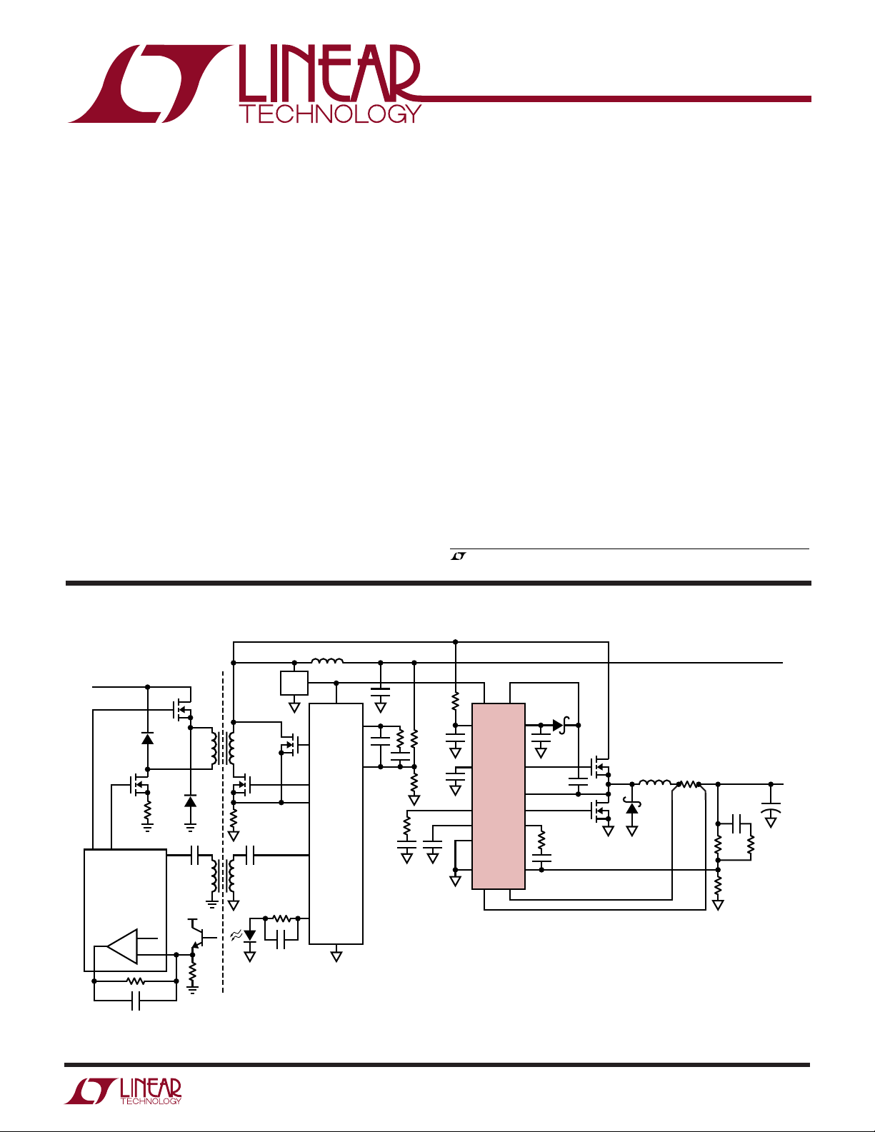
TYPICAL APPLICATIO
The LT®3710 is a high efficiency step-down switching
regulator intended for auxiliary outputs in single secondary winding, multiple output power supplies.
The LT3710 drives dual synchronous N-channel MOSFETs
and achieves high efficiency. With leading edge modulation, it operates well with either primary side peak current
or voltage mode control. It is synchronized to the falling
edge of the transformer secondary winding and can be
used in both single-ended and double-ended isolated
power converter topologies. A high speed operational
amplifier is incorporated to achieve optimum compensation and fast transient response. A user selectable discontinuous conduction mode improves light load efficiency.
The LT3710 is available in a thermally enhanced TSSOP-16
exposed pad power package.
, LTC and LT are registered trademarks of Linear Technology Corporation.
36V
TO 72V
+
220Ω
V
OUT1
3.3V
AT 10A
V
OUT2
1.8V
AT 10A
C
OUT2
3710 F01
L1
V
IN
••
BG
TG
V
C
LT3781
SG
V
REF
+
V
FB
–
ISOLATION
BOUNDARY
••
V
CC
BIAS
V
DD
V
COMP
CG
V
FB
FG
I
SNS
LTC1698
SYNC
OPTODRV
GND
: POSCAP, 680µF/4V
C
OUT2
L2: SUMIDA CEP125-IR8MC-H
Q1, Q2: SILICONIX Si7440DP
180pF
10k
10pF
680pF
10k
V
BOOST
CC
SYNC
LT3710
CSET
C
S
ILCOMP
SS
0.01µF
BGS
PGND
CL–CL
PLEASE REFER TO FIGURE 3
IN THE APPLICATIONS SECTION
FOR THE COMPLETE SCHEMATIC
GBIAS
SW
VA
OUT
V
CMDSH-3
4.7µF
L2
TG
0.1µF
BG
3.3k
33nF
FB
+
Q1
1.8µH
Q2 B340A
0.006Ω
4700pF
3.01k
2.32k
Figure 1. Simplified Single Secondary Winding 3.3V and 1.8V Output Isolated DC/DC Converter
3710f
1
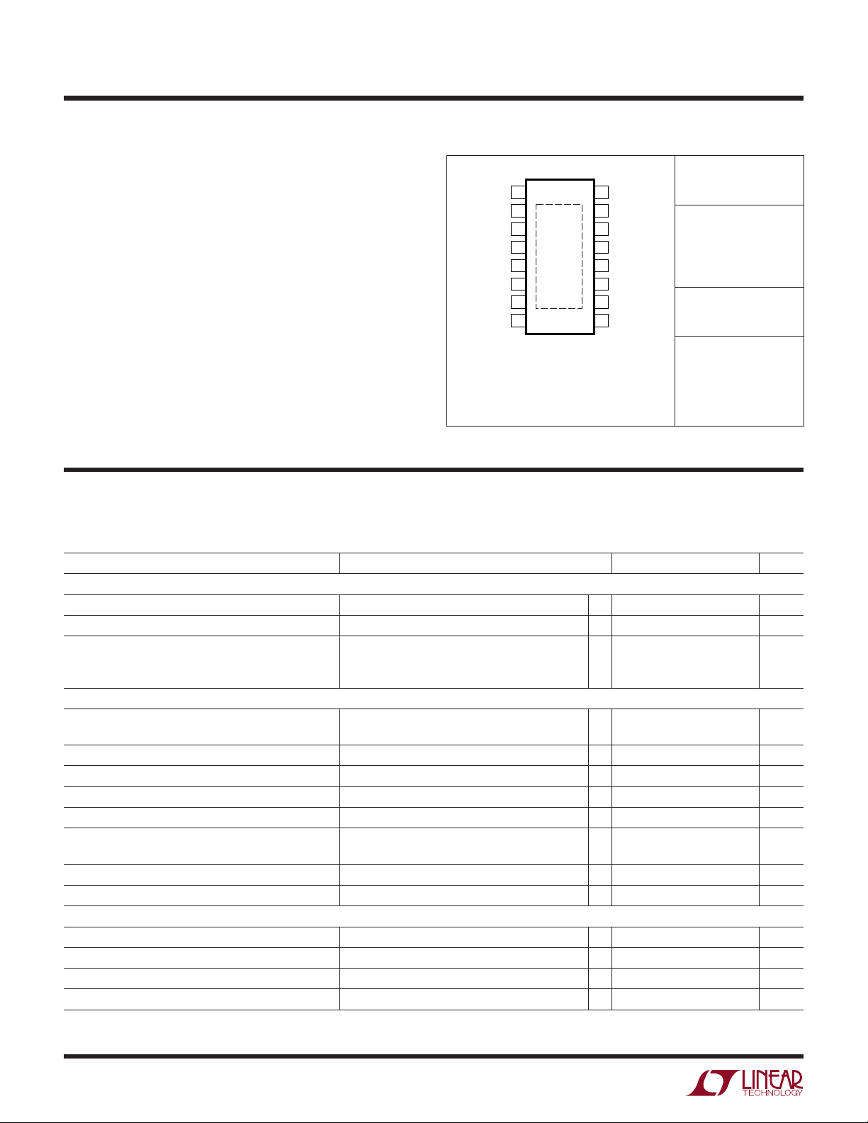
LT3710
1
2
3
4
5
6
7
8
TOP VIEW
FE PACKAGE
16-LEAD PLASTIC TSSOP
16
15
14
13
12
11
10
9
BOOST
TGATE
SW
CSET
SYNC
ILCOMP
SS
V
FB
GBIAS
BGATE
PGND
V
CC
CL
–
CL
+
VA
OUT
BGS
17
WW
W
ABSOLUTE AXI U RATI GS
U
UUW
PACKAGE/ORDER I FOR ATIO
(Note 1)
VCC Supply Voltage.................................................. 26V
BOOST Pin Voltage With Respect to SW pin ........... 10V
BOOST Pin Voltage With Respect to GND pin.......... 35V
SYNC Pin Voltage .................................................... 30V
ORDER PART
NUMBER
LT3710EFE
Operating Junction Temperature Range
(Notes 2, 3) ...................................... – 40°C to 125°C
Storage Temperature Range ................. –65°C to 150°C
Lead Temperature (Soldering, 10 sec)..................300°C
Note: If higher than 30V on SYNC pin is needed, add a 10k resistor in series with the pin.
FE PART
MARKING
3710EFE
T
= 125°C, θJA = 38°C/W
JMAX
EXPOSED PAD IS SGND (PIN 17) MUST BE
CONNECTED TO PGND AND SOLDERED TO PCB
Consult LTC Marketing for parts specified with wider operating temperature ranges.
ELECTRICAL CHARACTERISTICS
temperature range, otherwise specifications are at TA = 25°C. VCC = 11V, operating maximum VCC = 24V, no load on any outputs
unless otherwise noted.
The ● denotes the specifications which apply over the full operating
PARAMETER CONDITIONS MIN TYP MAX UNITS
Overall
Supply Voltage (VCC) ● 824V
Supply Current (I
Boost Pin Current V
) VA
VCC
≤ 1.2V (Switching Off) 7 12 mA
OUT
= VSW + 8V, 0V ≤ VSW ≤ 24V
BOOST
TGATE High 2 3 mA
TGATE Low 2 3 mA
Voltage Amplifier VA
Reference Voltage (V
FB Pin Input Current VFB = V
VA
High 4.5 V
OUT
VA
Low 0.8 V
OUT
VA
Source Current ● 100 300 µA
OUT
) 0.788 0.8 0.812 V
REF
REF
● 0.780 0.820 V
0.2 0.5 µA
Open-Loop Gain 100 dB
Gain Bandwidth Product 10 MHz
Soft-Start Current 51218 µA
Current Limit Amplifier CA1
Current Limit Threshold at (V
BGATE Off Threshold at (V
Switching Off Threshold at ILCOMP V
Input Current (CL+, CL–)V
+
–
– V
CL
+
– V
CL
) Common Mode Voltage from 0V to VCC – 2.5V ● 50 70 85 mV
CL
–
), BGS Pin Float Common Mode Voltage from 0V to VCC – 2.5V 0 8 15 mV
CL
ILCOMP
+
= V
CL
–
CL
100 µA
0.15 V
3710f
2
LT3710
ELECTRICAL CHARACTERISTICS
The ● denotes the specifications which apply over the full operating
temperature range, otherwise specifications are at TA = 25°C. VCC = 11V, operating maximum VCC = 24V, no load on any outputs
unless otherwise noted.
PARAMETER CONDITIONS MIN TYP MAX UNITS
Oscillator
Switching Frequency CS = 500pF (No SYNC) ● 170 200 240 kHz
C
= 333pF (No SYNC) ● 240 280 340 kHz
S
Synchronization Frequency Range CS = 500pF ● 245 400 kHz
C
= 333pF ● 345 500 kHz
S
CSET Ramp Valley Voltage CS = 1000pF (No SYNC) 0.90 1.15 1.4 V
CSET Peak-to-Peak Voltage CS = 1000pF (No SYNC) 2.4 V
Synchronization Pulse Threshold on SYNC Pin Falling Edge V
Maximum Duty Cycle VFB = V
SYNC
– 5mV, CS > 500pF ● 85 90 %
REF
Gate Drivers (TGATE, BGATE)
V
GBIAS
V
High (V
TGATE
V
High I
BGATE
V
Low (V
TGATE
V
Low I
BGATE
– VSW)I
TGATE
– VSW)I
TGATE
I
< 25mA ● 7.5 8.0 8.5 V
GBIAS
< 50mA, V
TGATE
< 50mA ● 5 6 7.5 V
BGATE
< –50mA ● 0.5 V
TGATE
< –50mA ● 0.5 V
BGATE
BOOST
= V
– 0.5V ● 567 V
GBIAS
Peak Gate Drive Current 10nF Load 1 A
Gate Drive Rise and Fall Time 1nF Load 25 ns
Note 1: Absolute Maximum Ratings are those values beyond which the life
of a device may be impaired.
Note 2: The LT3710E is guaranteed to meet performance specifications
from 0°C to 125°C. Specifications over the –40°C to 125°C operating
temperature range are assured by design, characterization and correlation
Note 3: This IC includes overtemperature protection that is intended to
protect the device during momentary overload conditions. Junction
temperature will exceed 125°C when overtemperature protection is active.
Continuous operation above the specified maximum operating junction
temperature may impair device reliability.
with statistical process controls.
2.5 V
UW
TYPICAL PERFOR A CE CHARACTERISTICS
V
vs I
GBIAS
Temperature ICC vs VCC (Switching Off)
8.1
8.0
(V)
7.9
GBIAS
V
7.8
7.7
0
over Junction
GBIAS
–40°C
25°C
125°C
10 20 26
I
(mA)
GBIAS
3710 G01
13
TA = 25°C
12
11
10
9
(mA)
CC
I
8
7
6
5
8 1012141618202224
VCC (V)
3710 G02
Voltage Amplifier VA Gain and
Phase
120
TA = 25°C
80
40
GAIN (dB)
0
–20
10
GAIN
0dB, 10MHz
100 1k 10k 100k 1M 10M 100M
FREQUENCY (Hz)
(–111°)
PHASE
–0
–50
PHASE (DEG)
–100
–150
–180
3710 G03
3710f
3
LT3710
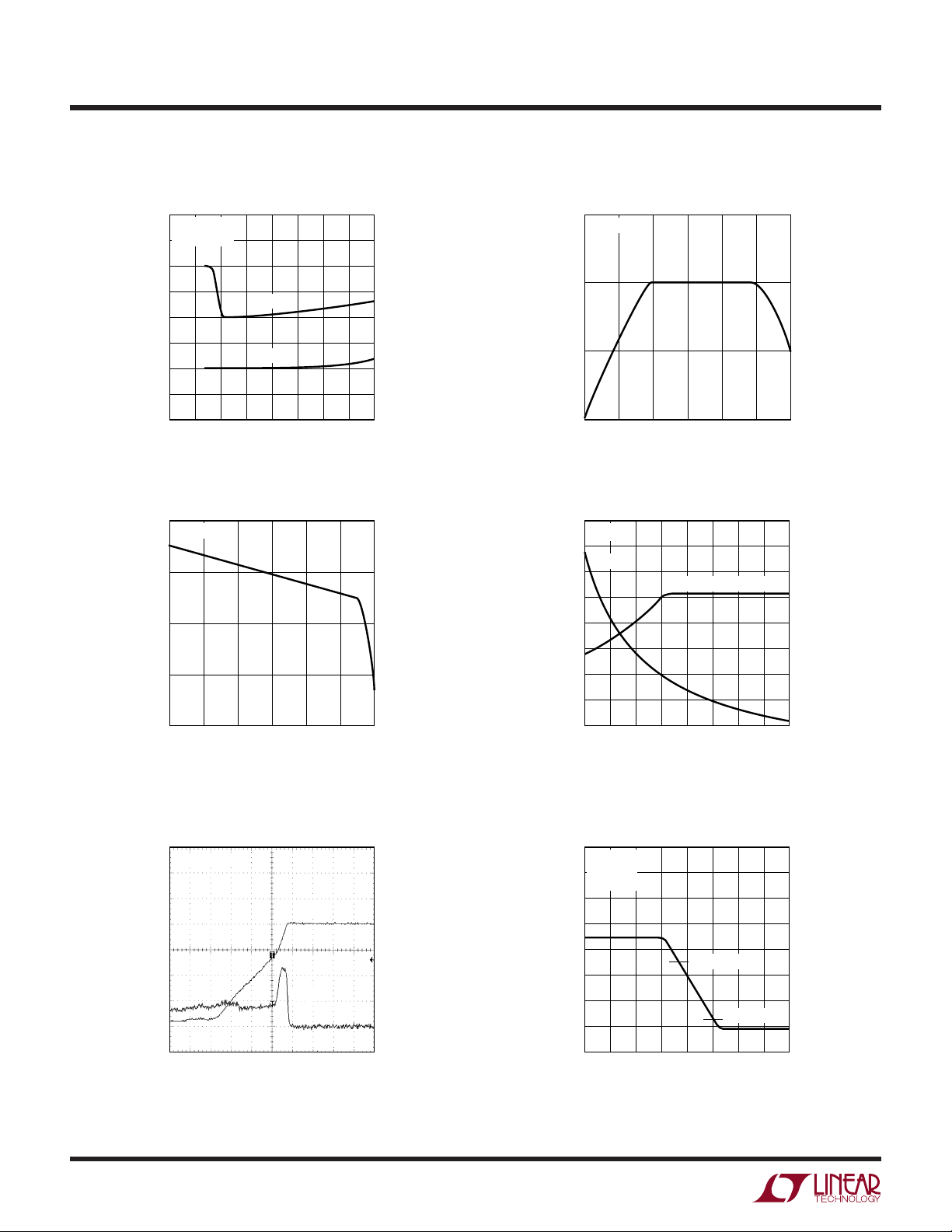
JUNCTION TEMPERATURE (°C)
–20–40 2507550 125
V
REF
(V)
0.801
0.800
0.799
0.798
3710 G05
CSET = 500pF
UW
TYPICAL PERFOR A CE CHARACTERISTICS
∆V
vs VCC, ∆FREQ vs V
(mV)
REF
∆V
–1
REF
CSET = 500pF
= 25°C
T
A
3
2
1
0
∆V
REF
∆FREQ
10 15 20 25
VCC (V)
CC
3710 G04
∆FREQ (kHz)
1
0
–1
V
vs Temperature
REF
Frequency vs Temperature
195
CSET = 500pF
200
205
210
SWITCHING FREQUENCY (kHz)
215
300
250
200
150
100
(mA)
GBIAS
I
–20–40 2507550 125
JUNCTION TEMPERATURE (°C)
G
vs I
BIAS
C
50
0
0
GBIAS
GBIAS
= 2.2µF
3710 G06
(Charging 2.2µF)
V
GBIAS
I
GBIAS
500µs
TIME
3710 G08
1ms
CSET vs Switching Frequency
500
TA = 25°C
CSET
400
300
FREQUENCY (kHz)
200
100
Current Limit Amplifier CA1 Gain
at VCC = 11V, V
8
VCC = 11V
= 5V
V
CLN
(V)
OUT
VA
7
= 25°C
T
A
6
5
4
3
2
1
0
12
10
8
V
GBIAS
6
(V)
4
2
0
MAXIMUM DUTY CYCLE
400200 600 800 1000
CSET (pF)
–
= 5V
CL
CSET PEAK
CSET VALLEY
6050 70 80 90
+
V
–
– V
(mV)
CL
CL
3710 G07
3710 G09
1.00
MAXIMUM DUTY CYCLE
0.95
0.90
0.85
0.80
0.75
0.70
4
3710f

UUU
PI FU CTIO S
LT3710
BOOST (Pin 1): Topside (Boosted) Driver Supply. This pin
is used to bootstrap and supply the topside power switch
gate drive circuitry. In normal operation V
from the internally generated 8V GBIAS, V
8.2V when TGATE is on.
TGATE (Pin 2): Topside (Boosted) N-Channel MOSFET
Driver. When TGATE is on, the voltage is equal to VSW + 6V.
SW (Pin 3): Switch Node Connection to Inductor.
CSET (Pin 4): Oscillator Timing Pin. The capacitor on this
pin sets the PWM switching frequency.
SYNC (Pin 5): Synchronization Input. This pin should be
connected to the secondary side output of the power
transformer with a series resistor. A filtering capacitor of
10pF is recommended.
ILCOMP (Pin 6): Current Limit Amplifier Compensation
Node. At current limit, CA1 pulls down on this pin to
regulate the output current.
SS (Pin 7): Soft-Start. A capacitor on this pin sets the
output ramp up rate. The typical time for SS to reach the
programmed level is (C • 0.8V)/10µA.
VFB (Pin 8): Voltage Amplifier Inverting Input. A resistor
divider to this pin sets the output voltage. Nominal voltage
at this pin is 0.8V.
BOOST
BOOST
is powered
= VSW +
BGS (Pin 9): Bottom Gate Switching Control. CA2 monitors the inductor current and prohibits BGATE from turning on when the inductor current is low (below 8mV across
the current sense resistor RS1) to allow discontinous
mode operation. Grounding this pin disables comparator
CA2.
VA
(Pin 10): Voltage Amplifier Output.
OUT
CL+ (Pin 11): Current Limit Amplifier Positive Input. The
threshold is set at 70mV.
CL– (Pin 12): Current Limit Amplifier Negative Input.
When used, CL– is connected to the output capacitor side
of the current + sense resistor and CL+ is connected to the
inductor side of the current sense resistor.
VCC (Pin 13): Supply of the IC. For proper bypassing, a low
ESR capacitor is required.
PGND (Pin 14): Ground of the Bottom Side N-Channel
MOSFET Driver.
BGATE (Pin 15): Bottom Side N-Channel MOSFET Driver.
GBIAS (Pin 16): 8V Regulator Output for Boostrapping
V
BOOST .
Exposed Pad (Pin 17): Connect to PGND (Pin 14).
A bypass capacitor of at least 2µF is needed.
3710f
5

LT3710
–
+
A11
A6
A2
SS
SW
1.6V
+
8mV
+
+
–
A10
+
–
PWM
3.5V
+
+
–
2.5V
+
70mV
–
+
A8
7V
+
8V
+
+
–
VA
+
–
CA1
A5
+
–
A3
BGATE
2.5V
+
A4
A1
TGATE
2
SW
3
GBIAS
C3
2µF
D3
16
BOOST
1
R1
BGATE
15
PGND14BGS
9
R2
2V
M1
L1
I
L
R
S1
M2
C2
0.3µF
CL
+
11
CL
–
12
VA
OUT
10
V
FB
8
SYNC
5
CSET
4
7
R3
R4
C4
2nF
R5
2k
C1
500pF
C
OUT
100µF
V
OUT2
D6
D4
I
1
10µA
5V
D7
V
REF
0.8V
C7
5nF
SS
C5
500pF
NOTE: EXPOSED PAD (PIN 17) IS SGND
AND MUST BE CONNECTED TO PGND (PIN 14).
SGND
CS10pF
C8
2µF
R8
R7
V
S
A7
E4
+
–
8V
+
V
CC
13
ONE
SHOT
OSC
RS
RESET
+
–
CA2
ILCOMP
6
R6
5k
C6
100pF
3710 BD
+
D5
D2
Q1
I2200µA
E2
SHUTDOWN
R
S
10k
D1
I
O
17
BLOCK DIAGRA
W
6
3710f

OPERATIO
LT3710
U
To generate isolated multiple outputs, most systems use
either multiple secondary windings or cascade regulators
for each additional output. Multiple secondary windings
sacrifice regulation of the auxiliary outputs. Cascaded
regulators require a larger inductor for the main output,
because all of the power is processed in series.
By generating the auxiliary output(s) from the secondary
winding of the main output, the LT3710 allows for parallel
processing of the output power. This minimizes the main
output inductor size and directly regulates the auxiliary
output. With synchronous rectification, the system efficiency is greatly improved.
Refering to the Block Diagram, the LT3710 basic functions
include a voltage amplifier, VA, to regulate the output
voltage to within typically 1.5%, a voltage mode PWM with
trailing edge synchronization and leading edge modulation, a current limit amplifier, CA1, and high speed synchronous switch drivers.
During normal operation (see Figure 2), a switching cycle
begins at the falling edge of the transformer secondary
voltage VS. The internal oscillator is reset, turning off the
top MOSFET M1 and turning on the bottom MOSFET M2.
During this portion of the cycle, the inductor current is
discharged by the output voltage V
. The transformer
OUT2
secondary voltage VS will go high during this portion of the
cycle. Since M1 is off, the switch node voltage V
SW
remains zero. The inductor current continues to be discharged by the output voltage V
. This condition lasts
OUT2
until the ramp signal intersects the feedback error amplifier output VA
. The top MOSFET M1 turns on, pulling
OUT
the switch node voltage to VS. The inductor current of the
LT3710 circuit is then charged by VS – V
. The effective
OUT2
on time of this buck circuit ends when the secondary
voltage becomes zero. The next cycle repeats.
The ideal equation for duty cycle of the LT3710 is:
D2 = V
OUT2/VSP
where V
is the auxiliary output voltage, VSP is the
OUT2
amplitude of the secondary voltage and D2 is the duty
cycle of the switching node voltage VSW, as defined in
Figure 2.
V
RESET
T
D1T
TRANSFORMER
SECONDARY VOLTAGE
SYNC SIGNAL V
RAMP V
SWITCH NODE V
Figure 2. Leading Edge Modulation,
Trailing Edge Synchronization
RESET
CSET
VA
OUT
TGATE
BGATE
V
S
I
L
T
SW
D2T
3710 F02
V
SP
V
SP
U
WUU
APPLICATIO S I FOR ATIO
Synchronization and Oscillation Frequency Setting
The switching is synchronized to the secondary winding
falling edge and the synchronization threshold is typically
2.5V. The synchronization falling edge triggers an internal
inverted ramp (see Figure 2) and starts a new switching
cycle for the leading edge voltage mode PWM. The reason
for using leading edge modulation is to keep the transformer primary side peak current sensing undisturbed.
For proper synchronization, the oscillator frequency should
be set lower than the system switching frequency with
tolerances taken into account.
f
< (fSL • 0.8)
OSC
f
is the low limit of the system switching frequency and
SL
0.8 is the tolerance of f
OSC
.
For example, a system of 200KHz with 15% tolerance,
then fSL = 200k • 85% = 170kHz; and f
f
should be set below 136kHz.
OSC
Once f
CSET = (107250pf/f
For f
is determined, CSET can be calculated by
OSC
OSC(kHz)
= 100kHz, CSET = 1022.5pF.
OSC
) – 50pF.
< (170k • 0.8),
OSC
3710f
7

LT3710
U
WUU
APPLICATIO S I FOR ATIO
Output N-Channel MOSFET Drivers
The LT3710 employs high speed N-channel MOSFET
synchronous drivers to achieve high system efficiency.
GBIAS is the 8V regulator output to bias and supply the
drivers and should be properly bypassed with a low ESR
capacitor to ground plane. A Schottky catch diode is
required on the switch node.
Light Load Operation
If the BGS pin is grounded, the LT3710 stays in continuous
mode independent of load condition except in soft-start
operation (see Soft-Start section). If the BGS pin is left
open, under light load and V
will be turned off(see comparator CA2 of Block Diagram)
and the LT3710 goes into discontinous mode operation.
Current Limit
Current limit is set by the 70mV threshold across CL+ and
CL–, the inputs of the amplifier CA1. By connecting an
external resistor RS1(see Block Diagram), the current
limit is set for 70mV/RS1. R6 and C6 stablize the current
limit loop. If current limit is not used, both CL+ and CL
should be grounded and the BGS pin should also be
grounded to disable comparator CA2.
Soft-Start and Shutdown
During soft-start, VSS is the reference voltage that controls
the output voltage and the output ramps up following VSS.
The effective range of VSS is from 0V to V
time for the output to reach the programmed level is
(C • 0.8V)/10µA.
During start up, BGATE will stay off until VSS gets up to
1.6V. This prevents the bottom MOSFET from turning on
if the output is precharged.
To shut down the LT3710, the SS pin should be pulled
below 50mV by a VN2222 type N-channel transistor. Note
that during shutdown BGATE will be locked off when V
drops below 0.6V. This prevents the bottom MOSFET from
drops below 8mV, BGATE
RS1
. The typical
REF
–
SS
discharging the output, which would cause the output to
undershoot below ground.
Layout Considerations
For maximum efficiency, the switching rise and fall times
are less than 20ns. To prevent radiation, the power
MOSFETs, SW pin and input bypass capacitor leads should
be kept as short as possible. A ground plane should be
used under the switching circuitry to prevent interplane
coupling and to act as a thermal spreading path. Note that
the bottom metal of the package is the heat sink, as well as
the IC signal ground, and must be soldered to the ground
plane.
Output Voltage Programming
The feedback reference voltage is 0.8V. The output voltage
can be easily programmed by the resistor divider, R3 and
R4, as shown in the Block Diagram.
R
3
V
Filtering on the SYNC Input
It is necessary to add RC filtering on the SYNC input of the
LT3710 to eliminate the negative glitch at the turn on of the
top MOSFET. When the top MOSFET M1 turns on, the
transformer secondary current instantly changes from the
original first output inductor current to the sum of two
output inductor currents. The high di/dt on the transformer leakage inductance causes the transformer secondary voltage VS to drop for a short interval. If the leakage
inductance is large enough, the VS dip will be lower than
the synchronization threshold (about 2.5V), falsely triggering the synchronization. The top MOSFET is turned off
immediately. As a result, the output voltage will not be
regulated properly.
A filter circuit is needed to ensure proper operation. A
small RC filter with RS = 10k and CS = 10pF are typical.
=+
OUT2
08 1
.•
R
4
8
3710f

LT3710
U
WUU
APPLICATIO S I FOR ATIO
Output Inductor Selection
The key parameters for choosing the inductor include
inductance, RMS and saturation current ratings and DCR.
The inductance must be selected to achieve a reasonable
value of ripple current, which is determined by:
12•
VD
∆=
OUT2
I
L
Typically, the inductor ripple current is designed to be
20% to 40% of the maximum output current.
The RMS current rating must be high enough to deliver the
maximum output current. A sufficient saturation current
rating should prevent the inductor core from saturating.
These two current ratings can be determined by:
II
≥+
RMS O
II
≥+
SAT O
−
()
•
fL
2
I
∆
2
LMAX
12
I
∆
LMAX
2
The R
of the MOSFETs should be selected to deliver
DS(ON)
the required current at the desired efficiency as well as to
meet the thermal requirement of the MOSFET package.
The conduction power losses of the MOSFETs are:
PM1 ≅ I
PM2 ≅ I
2
O
2
O
• R
• R
DS(ON)M1
DS(ON)M2
• D2
• (1 – D2)
where IO is the maximum output current of LT3710 circuit,
R
DS(ON)M1
and bottom MOSFETs, respectively. The R
and R
DS(ON)M2
are the on-resistance for the top
must be
DS(ON)
determined with 6.5V gate drive and the expected operating temperature.
A good number of high performance power MOSFET
selections are available from Siliconix, International Rectifier and Fairchild. If the V
DSS
and R
ratings are the
DS(ON)
same, the MOSFETs with the lowest gate charge QG should
be chosen to minimize the power loss associated with the
MOSFET gate drives, the switching transitions and the
controller bias supply.
Output Capacitor Selection
where IO is the maximum output current and ∆I
LMAX
is the
maximum peak-to-peak inductor ripple current.
To optimize the efficiency, we usually choose the inductor
with the minimum DCR if the inductance and current
ratings are the same.
Power MOSFET Selection
The LT3710 drives two external N-channel MOSFETs to
deliver high currents at high efficiency. The gate drive
voltage is typically 6.5V. The key parameters for choosing MOSFETs include drain to source voltage rating V
and R
at 6.5V gate drive. Note that the transformer
DS(ON)
DSS
secondary voltage waveform will overshoot at its rising
edge due to the ringing between transformer leakage
inductance and parasitic capacitance. The V
DSS
of both
top and bottom MOSFETs must be sufficiently higher
than the maximum overshoot. It is recommended that an
RC snubber or a voltage clamping circuitry be placed
across the transformer secondary winding to limit the V
S
overshoot.
The selection of the output capacitor is determined by the
output ripple and load transient requirements. In low
output voltage applications, always choose capacitors
with low ESR. The output ripple voltage is approximated
by:
∆≈∆ +
V I ESR
OUT L
8
fC
1
OUT
where ∆IL is the inductor peak-to-peak ripple current.
A partial list of low ESR high performance capacitor types
includes SP capacitors from Panasonic and Cornell Dubilier,
POSCAPs and OS-CON capacitors from Sanyo, T510 and
T520 surface mount capacitors from Kemet.
Design Example
Figure 3 shows an application example for the LT3710. It
is a dual output, high efficiency, isolated DC/DC power
supply with 36V to 72V input, 3.3V/10A and 1.8V/10A
outputs. The basic power stage topology is a 2-transistor
3710f
9

LT3710
V
CC
13
2
1
5
1µF 82pF
1nF
OVLO
SHDN
1.24k
73.2k
20k
11V
MMSZ5241B
FZT
853
B0540W
10k
1N4148
270k
4.7µF
5V
REF
6
F
SET
4.7nF
8
SS
10
14
BAS21
BAT54
T2
PULSE
P2033
BAS21
BAT54
BAT54
ZVN3310F
9
V
C
PGND
V
FB
374
THERM
LT3781
SYNC SGND
52.3k
1%
10Ω
1k
3k
1k
470Ω
4.7k
2k
FZT690B
4.7µF
0.22µF
NOTE UNLESS NOTED:
ALL CAPS 25V
ALL RESISTORS 0.1W, 5%
Q1, Q2 SILICONIX Si7456DP
V
CCS
CMPZ5240B
10V
1
3.3Ω
5V
REF
7
143
1
4
8
7
5
14
15
6
5
82
3.3nF
4.7nF
0.1µF
5V
REF
12
SG
0.1µF
ON/OFF
11
SENSE
15
BG
18
BSTREF
19
TG
20
BAS21
DO1608C-105
V
BST
220pF
1.5µF
100V
1.2µH
COILCRAFT
D01813P-122HC
1.5µF
100V
22nF
1nF
••
SYNC V
FB
OVPIN
MARGIN
I
COMP
V
DD
OPTODRV
V
AUX
0.1µF
0.01µF
V
OUT1
12
I
SNS
11
I
SNSGND
16
FG
2
CG
PGND GND
LTC1698
PWRGD
6
8
9
7
13
1.24k
1%
1.78k
1%
2.43k
1%
1043
V
COMP
V
OUT1
TRIM
3710 F03a
3.01k
1%
B0540W
0.025Ω
1/2W
3
4
Q2
1nF
100V
2.2nF
250VAC
1nF
100V
Si7440DP
×2
Si7440DP
470µF
4V
POSCAP
MUR120S
MUR120S
2
7
5
•
••
1
Q1
T1
PULSE
PA0191
V
IN
+
V
IN
–
V
OUT1
+
3.3V
AT 10A
V
OUT
RTN
10Ω
10Ω
SEC
2.5µH
SUMIDA CEP125-2R5
+
470µF4VPOSCAP
+
1µF
B0540W
1µF
0.1µF
330pF
10k
U
APPLICATIO S I FOR ATIO
WUU
ee Next Page)
Figure 3a. 36V to 72V DC to 3.3V/10A and 1.8V/10A (or 2.5V/10A) Dual Output Isolated Power Supply-Basic Circuit (Part 1 of 2, S
10
3710f

LT3710
U
WUU
APPLICATIO S I FOR ATIO
forward converter with synchronous rectification. The
primary side controller uses an LT3781, a current mode
2-transistor forward controller with built-in MOSFET drivers. On the secondary side, an LTC1698 is used to provide
the voltage feedback for the 3.3V output, as well as the gate
drive for the synchronous MOSFETs. The error amplifier
output is fed into the optocoupler and then relayed to
LT3781 on the primary side to complete the 3.3V regulation. The 1.8V output is generated by the LT3710 circuit.
A planar transformer PA0191 built by Pulse Engineering is
employed as the power transformer in this design. This
transformer is constructed on a PQ20 core with a nine turn
primary winding, two turn secondary winding and seven
turn auxiliary winding for the LT3781 bias supply. Because
4.7µF
10pF
SEC
V
CCS
1µF
10k
0.01µF
C37 680pF
180pF
10k
5
7
13
4
14
6
17
BOOST
SYNC GBIAS
SS
V
CC
LT3710
CSET
PGND
ILCOMP
PGND
VA
OUT
10
0.033µF
16V
1
16
2
TGATE
3
SW
15
BGATE
9
BGS
11
+
CL
12
–
CL
V
FB
8
3.3k
CMDSH-3
CMDSH-3
0.01µF
the maximum secondary voltage VSP is about 16V, 30V
MOSFETs are chosen with the consideration that the
secondary voltage overshoot is typically 20% to 30% of
VSP. In this particular design, Si7440DP is selected due to
its low R
SD(ON)
, 30V V
rating and its compact and
DSS
thermally enhanced PowerPak SO-8 package.
The switching frequency of the circuit is about 230kHz.
1500V input to output isolation is provided. Additional
features of this design include primary side on/off control,
±5% secondary side trimming on the 3.3V output, input
overvoltage protection and undervoltage lockout. The
complete design will mount within a standard half brick PC
board with about half inch height.
0.1µF
16V
Si7440DP
10Ω
Si7440DP
1.8µH
SUMIDA
CEP125-IR8
B340A
0.006Ω
1%
3.01k
1%
+
4700pF
220Ω
680µF
4V
POSCAP
V
OUT2
1.8V/10A
680µF
+
4V
POSCAP
330pF
2.32k
1%
3710 F03b
Figure 3b. 36V to 72V DC to 3.3V/10A and 1.8V/10A Dual Output Isolated Power Supply (Part 2 of 2, See Previous Page)
3710f
Information furnished by Linear Technology Corporation is believed to be accurate and reliable.
However, no responsibility is assumed for its use. Linear Technology Corporation makes no representation that the interconnection of its circuits as described herein will not infringe on existing patent rights.
11

LT3710
PACKAGE DESCRIPTIO
2.74
(.108)
U
FE Package
16-Lead Plastic TSSOP (4.4mm)
(Reference LTC DWG # 05-08-1663)
Exposed Pad Variation BA
4.90 – 5.10*
(.193 – .201)
2.74
(.108)
16 1514 13 12 11
10 9
6.60 ±0.10
4.50 ±0.10
0.09 – 0.20
(.0036 – .0079)
NOTE:
1. CONTROLLING DIMENSION: MILLIMETERS
2. DIMENSIONS ARE IN
3. DRAWING NOT TO SCALE
RELATED PARTS
2.74
(.108)
SEE NOTE 4
0.45 ±0.05
1.05 ±0.10
0.65 BSC
RECOMMENDED SOLDER PAD LAYOUT
4.30 – 4.50*
(.169 – .177)
0.45 – 0.75
(.018 – .030)
MILLIMETERS
(INCHES)
1345678
2
° – 8°
0
0.65
(.0256)
BSC
0.195 – 0.30
(.0077 – .0118)
4. RECOMMENDED MINIMUM PCB METAL SIZE
FOR EXPOSED PAD ATTACHMENT
*DIMENSIONS DO NOT INCLUDE MOLD FLASH. MOLD FLASH
SHALL NOT EXCEED 0.150mm (.006") PER SIDE
0.05 – 0.15
(.002 – .006)
2.74
(.108)
1.10
(.0433)
MAX
FE16 (BA) TSSOP 0203
6.40
BSC
PART NUMBER DESCRIPTION COMMENTS
LT1339 High Power Synchronous DC/DC Controller Operation Up to 60V Maximum
LT1425 Isolated Flyback Switching Regulator General Purpose with External Application Resistor
LT1431 Programmable Reference 0.4% Initial Voltage Tolerance
LT1680 High Power DC/DC Step-Up Controller Operation Up to 60V Maximum
LT3781 Dual Transistor Synchronous Forward Controller Operation Up to 72V Maximum
LT1725 General Purpose Isolated Flyback Controller Drives External Power MOSFET with External I
SENSE
Resistor
LT1737 High Power Isolated Flyback Controller Sense Output Voltage Directly from Primary-Side Winding
LT1950 PWM Controller for Flyback, Forward and SEPIC 15W to 500W, Isolated and Nonisolated Power Supply 50% Smaller
Applications Transformer, Protects MOSFET
LT3804 Secondary Side Dual Output Controller Regulates Two Outputs, Optocoupler Feedback Driver and Second Output
with Optodriver Synchronous Driver Controller
LT/TP 0803 1K • PRINTED IN USA
12
Linear Technology Corporation
1630 McCarthy Blvd., Milpitas, CA 95035-7417
(408) 432-1900 ● FAX: (408) 434-0507
●
www.linear.com
LINEAR TECHNOLOGY CORPORA TION 2002
3710f
 Loading...