

Page 1
µPower Buck Regulator Safely Rides Through Automotive
Load Dumps – Design Note 475
Juan G. Aranda
Introduction
W h e n a b u c k r e g u l a t o r i s u s e d i n a p p l i c a t i o n s w h e r e o u t p u t
s h o r t - c i r c u i t a n d o v e r l o a d c o n d i t i o n s o c c u r , t h e d u t y c y c l e
required to keep the inductor current under control can
be lower than the regulator’s minimum duty cycle when
operating at full speed. Therefore, to effectively protect a
traditional regulator under such conditions, its switching
frequency must be reduced to a speed that can safely
handle the maximum expected input voltage.
In some cases, frequency foldback can help reduce the
effective duty cycle by reducing the switching frequency
as the output voltage falls out of regulation. However,
this technique might not provide enough protection if the
folded frequency is not low enough. In the end, the duty
cycle problem imposes a limit on the maximum switching
frequency at which the regulator can be safely operated,
especially in automotive applications where the input
supply can see positive voltages several times higher
than the normal 12V operating voltage.
®
The LT
3682 is a new 1A buck regulator that overcomes
the dut y cycle limitation by monitoring t he current t hrough
the external catch diode, and delaying the generation
of new switch pulses if this current exceeds a defi ned
value. The LT3682 safely accommodates output shorts
and overload conditions up to its maximum adjustable
operating frequency of 2.2MHz regardless of input voltage. This added level of protection allows automotive
systems designers to take advantage of the maximum
switching frequency of the regulator without concern for
transients on the input supply.
The LT3682 accepts input voltages from 3.6V to 36V and
transients up to 60V. Additional features such as softstart, power good fl ag, frequency foldback and thermal
shutdown are all included in the thermally enhanced
12-lead 3mm × 3mm DFN package.
Minimum Switch On-Time
Under normal load conditions the internal switch current
limit is regulated to meet the required peak inductor current. Due to intern al delays, the power switch does not turn
off immedia tely when the internal current limi t is reached,
but instead t akes the minimum on-time (t
ON(MIN)
) to do so.
This delay allows the inductor current to continue rising
to values that depend on the current slope and the value
of t
ON(MIN)
. During positive input voltage transients the
slope of the rising inductor current is greatly increased,
thus raising its p eak value. A well designed buck converter
must sk ip swi tc h pulse s to ma int ai n re gulat ion i f th e new
duty cycle requirements cannot be met due to minimum
on-time limitations.
Overload conditions during the input transients may aggravate the situation further. Under extreme overloads
the internal current limit is ultimately clamped to its
maximum value, I
, and the output voltage falls out of
LIM
regulation, reducing the negative slope of the inductor
L, LT, LTC, LTM, Linear Technology and the Linear logo are registered trademarks of
Linear Technology Corporation. All other trademarks are the property of their respective
owners.
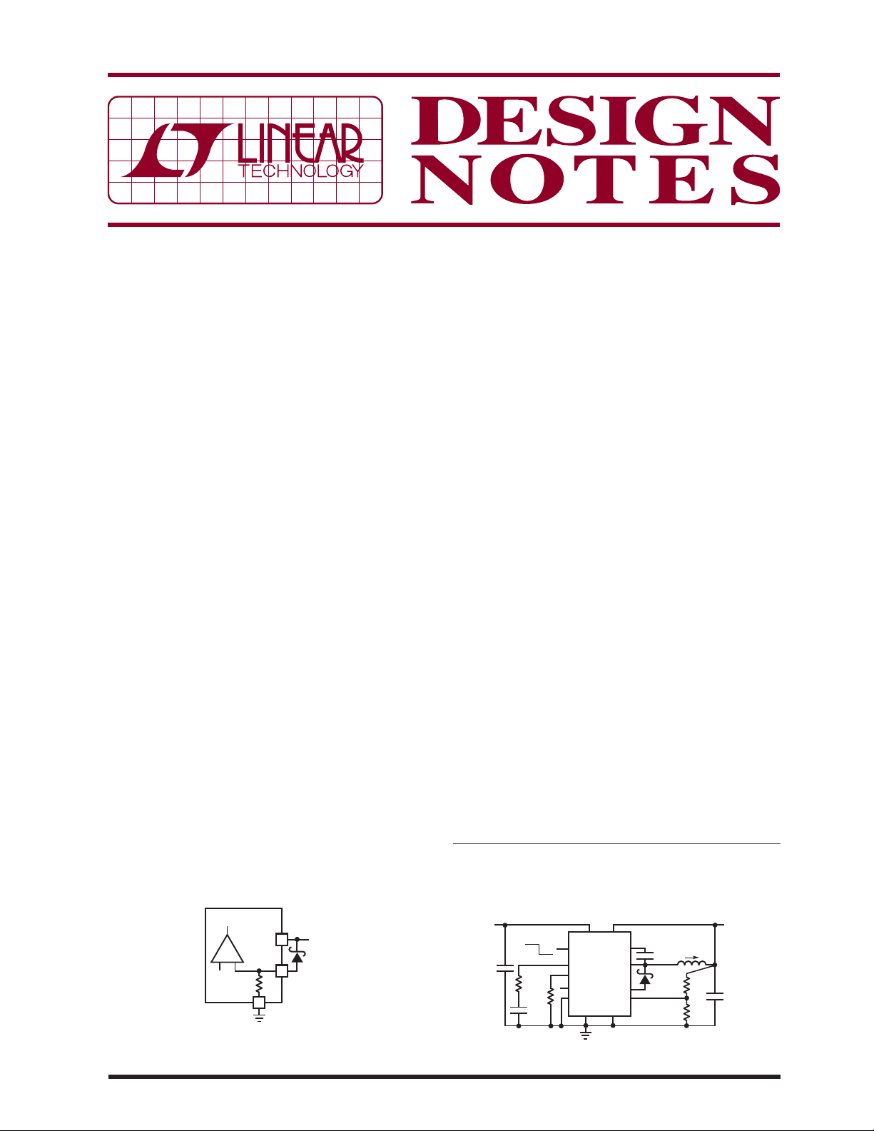
SW INHIBIT
V
LT3682
SW
+
–
R
SENSE
PGND
DA
DN475 F01
IDA
CATCH
DIODE
Figure 1. The LT3682 Monitors the Current Flowing
Through the External Catch Diode at the DA Pin
02/10/475
6.9V TO 36V
TRANSIENT
TO 60V
2.2μF
V
IN
BD
V
IN
RUN/SS BOOST
OFFON
C
IN
16.2k
40.2k
470pF
LT3682
V
C
R
T
PG
SYNC
GND PGND
f = 800kHz
0.22μF
SW
B150
DA
FB
Figure 2. A Typical 800kHz Application
10μH
L
536k
102k
DN475 F02
V
OUT
5V
0.9A, V
1A, V
C
OUT
10μF
6.9V
IN
12V
IN
Page 2
current accordingly. If during the switch off-time the
inductor current does not return to the same or smaller
values it had at the end of the previous cycle, its peak
value will ratchet higher in every cycle and increase to
unacceptably high levels.
Monitoring Current Via the DA Pin
The LT3682 constantly monitors the inductor current
during the switch off-time by looking at the current fl owing through the external catch diode via the DA (diode
anode) pin (see Figure 1) and delays the generation of
new switch pulses if this current does not fall below a
defi ned threshold, I
, thus reducing the regulator’s ef-
DA
fective duty cycle.
Thus, it is now possible to use th e small footprint inductors
found in high frequency applications without sacrifi cing
robustness during a number of fault conditions. Figures 2
and 5 show how to confi gure the LT3682 in a 5V
OUT
application with a 800kHz and 1.7MHz programmed
switching frequency, respectively. The resistive load at
is increased until the regulator hits its maximum
V
OUT
current limit. Figures 3, 4, 6 and 7 show the DA pin current sense protection for input voltages of 12V and 36V
for both applications. In all cases the lowest value of the
inductor current is pinned to about 1.1A, which keeps its
peak value well under control. By delaying the generation
of new switch pulses the switching frequency is effectively reduced to satisfy the new duty cycle requirements
introduced by the fault condition.
V
OUT
2V/DIV
I
L
1A/DIV
V
SW
20V/DIV
1μs/ DIV
Figure 3. The 800kHz Application with VIN = 12V. Overload
Condition Forces V
V
OUT
2V/DIV
I
L
1A/DIV
V
SW
20V/DIV
to Drop to About 3.2V
OUT
1μs/ DIV
Figure 4. The 800kHz Application with VIN = 36V. Overload
Condition Forces V
to Drop to About 3.5V
OUT
0V
0A
0V
DN475 F03
0V
0A
0V
DN475 F04
Conclusion
The LT3682 is a 1A monolithic buck switching regulator that accepts input voltages from 3.6V to 36V and
transients up to 60V. It features an adjustable and
synchronizable switching frequency from 250kHz to
2.2MHz. It also has the ability to monitor the current
fl owing through the external catch diode, thus providing
an extr a level of protection against out put faul t conditions
over the entire operating frequency range, regardless of
input voltage. These features, together with its typical
75μA no load quiescent current makes the LT3682 the
right choice in high frequency automotive and batterypowered applications.
V
IN
9V TO 19.5V
TRANSIENT
TO 60V
C
2.2μF
IN
OFFON
13.3k
13.7k
680pF
Figure 5. A Typical 1.7MHz Application
V
OUT
2V/DIV
I
L
1A/DIV
V
SW
20V/DIV
Figure 6. The 1.7MHz Application with VIN = 12V.
Overload Condition Forces V
V
OUT
2V/DIV
I
L
1A/DIV
V
SW
20V/DIV
Figure 7. The 1.7MHz Application with VIN = 36V.
Overload Condition Forces V
BD
V
IN
RUN/SS BOOST
LT3682
C
T
GND PGND
f = 1.7MHz
500ns/DIV
SW
V
R
PG
SYNC
OUT
500ns/DIV
OUT
L
4.7μH
0.22μF
B150
DA
FB
536k
102k
DN475 F05
0V
0A
0V
DN475 F06
to Drop to About 4.4V
0V
0A
0V
DN475 F07
to Drop to About 4.4V
V
OUT
5V
0.9A
C
OUT
10μF
Data Sheet Download
www.linear.com
Linear Technology Corporation
1630 McCarthy Blvd., Milpitas, CA 95035-7417
(408) 432-1900
●
FAX: (408) 434-0507 ● www.linear.com
For applications help,
call (408) 432-1900, Ext. 3513
dn475 LT/TP 0210 116K • PRINTED IN THE USA
© LINEAR TECHNOLOGY CORPORATION 2010
 Loading...