

36V 2A Buck Regulator Integrates Power Schottky
Design Note 412
David Ng
Introduction
Everyone wants more power in less space. However, the
task of designing a power supply is easy to describe but
d i f fi c u l t t o e x e c u t e . H o w d o e s a d e s i g n e r s e l e c t a n o p t i m a l
set of components that yields the best possible power
supply in terms of size, cost and performance? Well, it
is easier if the selection is reduced to only a handful of
components.
®
For instance, the LT
3681 reduces parts selection to only
a few passive components by integrating all of the power
semiconductors necessary to make a buck converter
into a single package. Don’t think that this high level of
integration limits the usefulness of this part. The LT3681
accepts inputs from 3.6V to 34V, provides excellent line
and load regulation and dynamic response, and offers a
high effi ciency solution over a wide lo ad range while keep-
®
ing the output ripple low during Burst Mode
operation.
Furthermore, its frequency is adjustable from 300kHz to
2.8MHz, enabling the use of small, low cost inductors
and ceramic capacitors.
V
IN
6.3V TO
34V
OFF ON
20k
4.7µF
330pF
60.4k
L: TAYIO YUDEN NP06DZB6R8M
RUN/SS BOOST
V
C
RT
PG
f = 800kHz
V
IN
LT3681
GND
BD
SW
DC
DA
BIAS
6.8µH
0.47µF
FB
590k
200k
A Small, Simple Solution
The LT3681 integrates a wide input voltage range, high
performance buck controller, power switch, high side
bootstr apping boost diode and a power Schottk y diode. All
of these attributes are
effi cient 14-pin 3mm × 4mm DFN package. So, all a designer needs to implement a full-fe atured buck converter
is to add the output LC fi lter and a few passives.
The most obvious adv antage of having the power Schot tky
d io d e i nt eg ra te d i n to th e LT 3 6 81 i s s pa c e s av in gs , r e du cing the amount of board space required by the complete
regulator by 15% or more. Moreover, the power Schottky
diode has been optimized for the intended operation of
the LT3681, so there is no need to agonize over fi nding
the perf ect form, fi t and function diode for t he application.
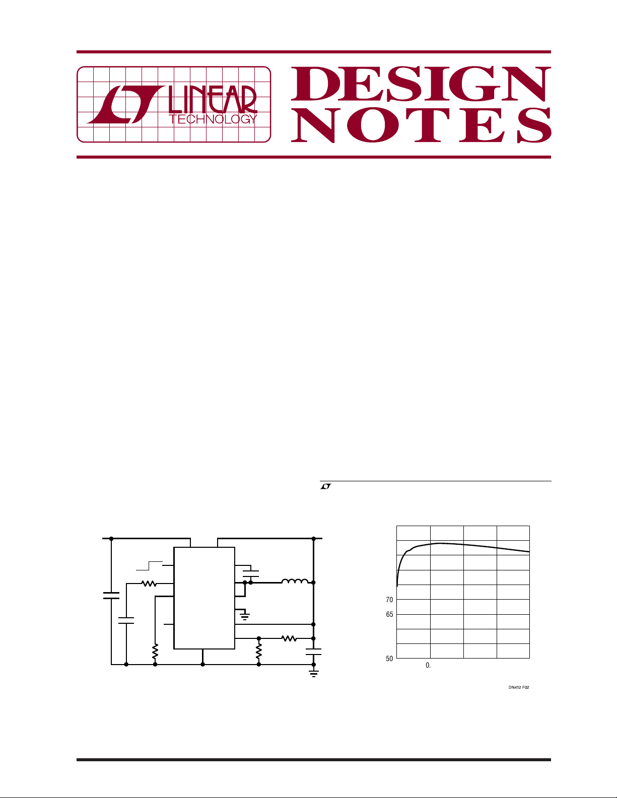
Figure 1 shows a schematic of the LT3681 producing 5V
at 2A from an input of 6.3V to 34V and Figure 2 shows
the effi ciency for a 12V input.
, LT, LTC, LTM and Burst Mode are registered trademarks of Linear Technology
Corporation. All other trademarks are the property of their respective owners.
V
OUT
5V
2A
L
22µF
DN412 F01
Figure 1. The LT3681 Integrates All of the Power Semiconductors
Necessary to Make a Simple 2A Buck Converter
crammed into a tiny but thermally
95
90
85
80
75
70
EFFICIENCY (%)
65
60
55
50
0
0.5
Figure 2. The LT3681 Boasts High Effi ciency
(12V Input to 5V Output)
1
LOAD CURRENT (A)
1.5
2
03/07/412
Low Ripple and High Effi ciency Solution over a
Wide Load Range
The LT3681 switching frequency can be programmed
from 300kHz to 2.8MHz by using a resistor tied from
the RT pin to ground. The LT3681 offers low ripple Burst
Mode operation that maintains high effi ciency at light
loads while keeping the no load output voltage ripple
below 15mV
P-P
.
D u r i n g B u r s t M o d e o p e r a t i o n , t h e L T 3 6 8 1 i s a b l e t o d e l i v e r
current in as little as one cycle to the output capacitor
followed by sleep periods where all of the output power
is delivered to the load by the output capacitor. Between
bursts, all circuitry associated with controlling the output
switch is shut down, reducing the input supply current to
only 55µA. As the load current decreases toward no load,
the percentage of time that the LT3681 operates in sleep
mode increases and the average input current is greatly
reduced, so high effi ciency is maintained.
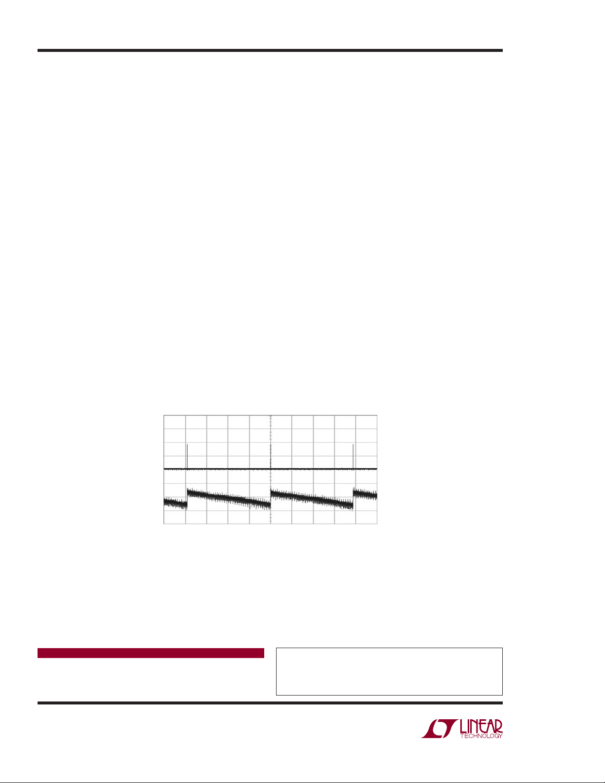
Figure 3 shows the low ripple and single cycle burst
inductor current at no load for the 3.3V regulator shown
in Figures 1 and 2. The LT3681 has a very low shutdown
current (less than 1µA), signifi cantly extending battery
life in applications that spend long periods in sleep or
shutdown mode.
For systems that rely on a well-regulated power source,
the LT3681 provides a power good fl ag that signals when
reaches 90% of the programmed output voltage.
V
OUT
A resistor and capacitor on the RUN/SS pin programs the
LT3681’s soft-start, reducing the inrush current during
star t-up. In applications w here the circuit is plugged into a
live input source through long leads, an electrolytic input
capacitor, which has higher ESR than a ceramic capacitor,
is recommended to dampen the overshoot voltage. Refer
to AN88 for further details.
Frequency Foldback Saves Chips
During short circuit, the LT3681 offers cycle-by-cycle
current limit and frequen cy foldback, which decrease s the
switching frequency. This increa ses the off time, reducing
the RMS current through the power switch and allowing
the inductor current to safely discharge before the next
switching cycle begins.
Conclusion
The robust design, small package and high level of integration of the LT3681 make it an excellent choice for a
wide variety of step-down applications where a compact
footprint and component optimization are critical. The
high input voltage rating, high power switch capability
and excellent package thermal conductivity adds to its
versatility.
INDUCTOR
CURRENT
200mA/DIV
OUTPUT
RIPPLE
10mV/DIV
Figure 3. This LT3681 Design Has Only 15mV of Output
Ripple, Even at No Load under Burst Mode Operation
Data Sheet Download
http://www.linear.com
Linear Technology Corporation
1630 McCarthy Blvd., Milpitas, CA 95035-7417
(408) 432-1900
●
FAX: (408) 434-0507 ● www.linear.com
500µs/DIV
DN412 F03
For applications help,
call (408) 432-1900, Ext. 2759
dn412f LT/TP 0307 305K • PRINTED IN THE USA
© LINEAR TECHNOLOGY CORPORATION 2007
 Loading...