

L DESIGN IDEAS
I
C N V V
N T
CHARGE
EFF FC UV
RECHARGE
=
( )
• –
•
V
IN
GND
V
OUT
LT3663 BUCK
GND
TOP RAIL
+
TOP ENA
TOP RAIL
–
BOT RAIL
+
BOT ENA
GND
BIAS
GND
TOP CAP
+
TOP CAP
–
BOT CAP
+
BOT CAP
–
GND
V
CAP
12V
GND
C
BOT
50F
C
TOP
50F
RUN
V
IN
GND
V
OUT
LT3663 BUCK
CONTROL
CIRCUIT
(FIGURE 3)
GND
RUN
V
IN
V
IN
ENA
I
LIM
RUN
V
OUT
V
OUT
2.65V
1.2A
I
SENSE
BOOST
SW
IR05H40CSPTR
L1
3.3µH
L1: TDK VLCF5020T-3R3N1R7-1
LT3663
GND FB
4.7µF
50V
1206
40V
2.0A
DFLS240
10k
R
ILIM
28.7k
0.1µF
16V
47µF
1206
16V
R
FB2
86.6k
R
FB1
200k
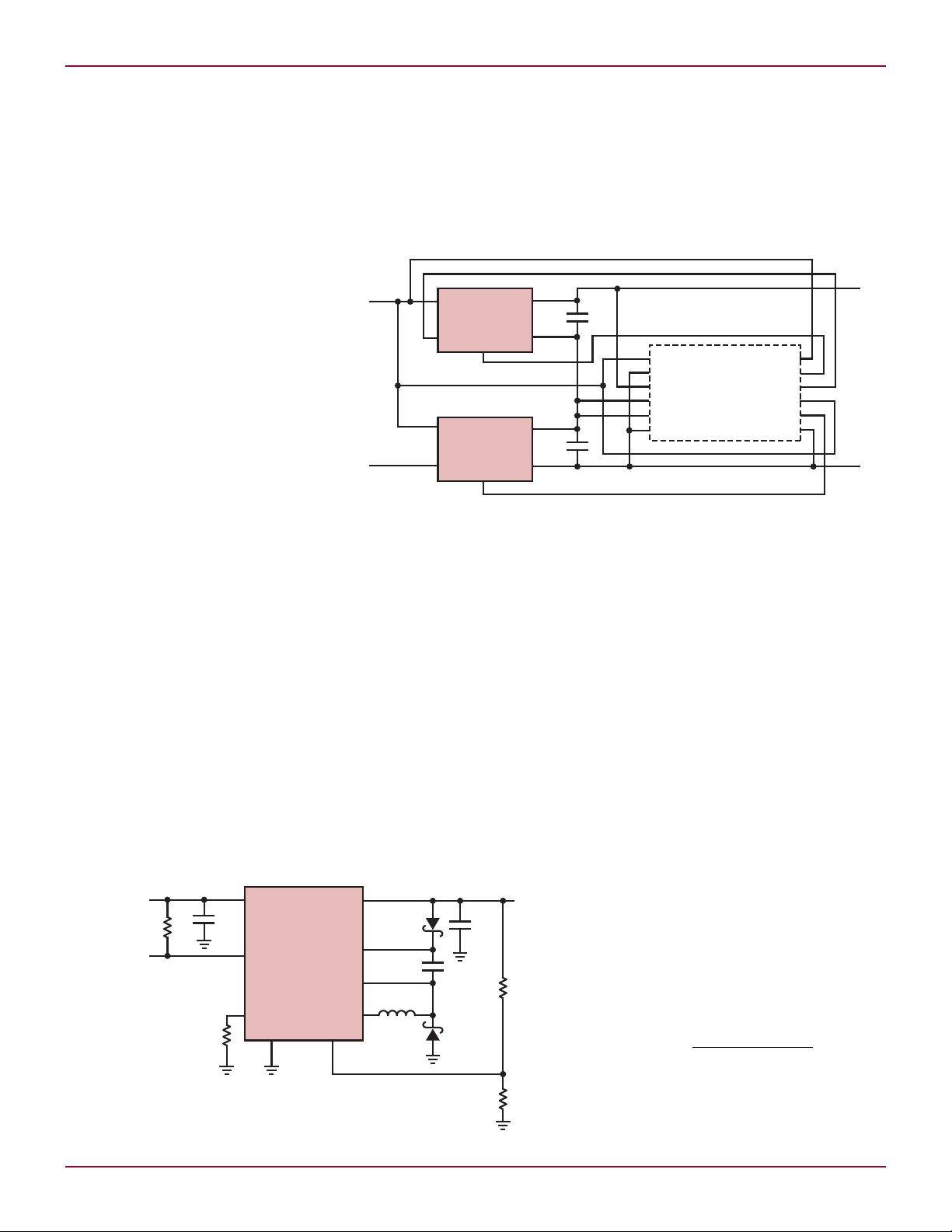
Supercapacitor Charger with
Adjustable Output Voltage and
Adjustable Charging Current Limit
Introduction
For applications using larger value
supercapacitors (tens to hundreds of
farads), a charger circuit with a relatively high charging current is needed
to minimize the recharge time of the
system. Supercapacitors are used as
energy hold up devices in applications
such as solid state RAID disks, where
information stored in high speed volatile memory must be transferred to
non-volatile flash memory when power
is lost. This transfer time may take
minutes, requiring hundreds of farads
to hold up the power supply until the
transfer is complete. The requirement
for the recharge time of these banks
of supercapacitors is typically less
than one hour. To accomplish this,
a high charging current is required.
This article describes a supercapacitor
charging circuit using the LT3663 that
meets these difficult requirements.
The LT3663 is a 1.2A, 1.5MHz stepdown switching regulator with output
current limit ideal for supercapacitor
applications. The part has an input
voltage range of 7.5V to 36V,has
adjustable output voltage and adjustable output current limit. The output
voltage is set with a resistor divider
network in the feedback loop while
the output current limit is set by a
single resistor connected from the I
30
30
Figure 2. Capacitor charger circuit using the LT3663
Figure 1. Block diagram for charging two supercapacitors in series
pin to ground. With its internal compensation network and internal boost
diode, the LT3663 requires a minimal
number of external components.
Power Ride-Through
Application
A procedure for selecting the size of
the supercapacitor is outlined in the
September 2008 edition of Linear
Technology, in an article titled “Replace Batteries in Power Ride-Through
Applications with Supercaps and
3mm × 3mm Capacitor Charger.” The
procedure determines the effective
supercapacitor (C
0.3Hz, based on the power level to
LIM
) capacitance at
EFF
by Jim Drew
be held up, the minimum operating
voltage of the DC/DC converter supporting the load, the distributed circuit
resistances including the ESR of the
supercapacitors, and the required
hold up time.
Once the size of the supercapacitor
is known, the charging current can
be determined to meet the recharge
time requirements. The recharge
time (T
RECHARGE
to recharge the supercapacitors from
the minimum operating voltage (VUV)
of the DC/DC converter to the full
charge voltage (VFC) of the supercapacitors. The voltage on the individual
supercapacitors at the start of the
recharge cycle is the minimum operating voltage divided by the number
(N) of supercapacitors in series. From
here on, this article describes an application with two supercapacitors in
series. The recharge current (I
is determined by the capacitor charge
control law:
This assumes that the voltage
across the supercapacitor doesn’t
discharge below the VUV/N value. This
assumption is valid if the time period
Linear Technology Magazine • June 2009
) is the time required
)
CHARGE
DESIGN IDEAS L
T
C V
I
CHARGE
EFF FC
CHARGE
=
•
IN OUT
BIAS
(FIGURE 1
CONNECTIONS)
(FIGURE 1
CONNECTIONS)
GND
BYP
GND
V
–
V
+
SHDN
U6
LT1761-3.3
3.3V
3.3V
3.3V
3.3V
10µF
16V
0.01µF
0.01µF
10µF
TOP ENA
TOP CAP +
TOP CAP
–
150k
V
REF
U7
LT1634-1.25
BOT_CHRG_L
100k 100k
100k 100k
OUT A V+
–IN A OUT B
–IN B
+IN B
+IN A
GND
0.1µF
–
+
U1
LT1784
V
–
V
+
3.3V
0.01µF
BOT CAP
+
BOT CAP
–
100k 100k
100k 100k
–
+
U2
LT1784
V
–
V
+
3.3V
0.01µF
100k
10k
1M
100k
R2
402k
R1
10k
R3
10k
R4
402k
1M
1k
1M
100k 100k
10k
–
+
U3
LT1784
0.01µF
TOP RAIL
–
U5
4N25
BOT ENA
2N7002
10k
GND
U4
LT6702
while input power isn’t available is
such that the supercapacitor’s leakage
current hasn’t significantly reduced
the voltage across the capacitor. The
voltage across the supercapacitor may
actually rise slightly after the DC/DC
converter shuts down due to the dielectric absorption effect. The initial charge
time T
for a fully discharged
CHARGE
bank of supercapacitors is:
Figure 1 shows a block diagram of
the components for this supercapacitor charger application.
Charging Circuit
Using the LT3663
To set the charging current, a resistor
R
is connected from the I
ILIM
the LT3663 to ground. Table 1 shows
the nominal charging currents for
various values of R
The full charge voltage is set by
the resistor divider network in the
.
ILIM
pin of
LIM
Figure 3. Charger control circuit
feedback loop. Table 2 shows various
full charge voltages versus the value
of R
ground) when resistor R
tied between the V
pin) is 200k. Figure 2 shows the charging circuit for each supercapacitor.
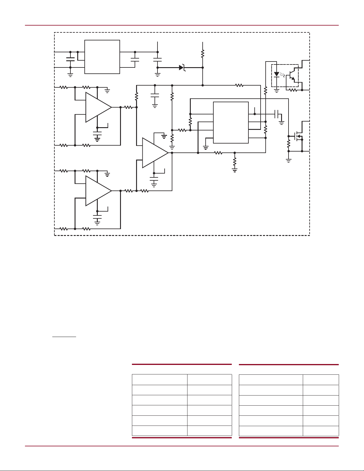
Control Circuit
(resistor from the FB pin to
FB2
pin and the FB
OUT
(resistor
FB1
for Charging Supercapacitors
The control circuit in Figure 3 is used
to balance the voltages of the supercapacitors while they are charging.
This is accomplished by prioritizing
Charging Current (A)
Table 1. Charging current vs R
0.4 140
0.6 75
R
Value (kΩ)
ILIM
0.8 48.7
1.0 36.5
1.2 28.7
ILIM
charge current to the lower voltage
supercapacitor—specifically by enabling the charging circuit for the
supercapacitor with the lower voltage
while disabling the circuit for the other
supercapacitor.
If the top charging circuit is enabled
while the bottom charging circuit is
disabled, the bottom supercapacitor
is charged by the input return current from the top charger. This return
current is a fraction of the charging
current so the top supercapacitor
charges faster. The control circuit
Full Charge Voltage (V)
Table 2. Full charge voltage vs R
2.65 86.6
2.5 93.1
2.4 100
2.2 115
2.0 133
continued on page 33
FB2
R
(kΩ)
FB2
Linear Technology Magazine • June 2009
3131

occurs at the midpoint of the avail-
V
OUT1
100mV/DIV
V
OUT2
100mV/DIV
V
OUT3
100mV/DIV
100µs/DIV
V
OUT1
1V/DIV
V
OUT2
1V/DIV
V
OUT3
1V/DIV
500µs/DIV
ENABLE TOP
ENABLE BOTTOM
ENABLE PINS
5V/DIV
V
C
TOP
500mV/DIV
0V
0V
0V
V
C
BOT
500mV/DIV
5s/DIV
C
TOP
= 50F
C
BOT
= 50F
INITIAL V
C
TOP = INITIAL VCBOT
ENABLE PINS
5V/DIV
V
C
TOP
500mV/DIV
0V
0V
0V
V
C
BOT
500mV/DIV
5s/DIV
C
TOP
= 50F
C
BOT
= 100F
INITIAL V
C
TOP < INITIAL VCBOT
ENABLE TOP
ENABLE BOTTOM
able output current range—ensuring
high efficiency under most operating
conditions. When the application enters low power mode, the converters
can be independently set to Burst
Mode operation to further improve
efficiency at light loads. In Burst Mode
operation, the total quiescent current
of the converters is reduced to 35µA.
During noise critical phases, Burst
Mode operation can be temporarily
forced to low noise by dynamically
driving the PWM pin high.
Supply Sequencing
Digital applications with multiple
supplies typically specify sequenced
start-up and shut-down of the supplies. Supply sequencing is important
to prevent powering up I/O pins that
are driven by unpowered core logic.
Without defined logic states, erratic
fluctuations may occur at the I/O pins.
LTC3521 provides individual control
of shutdown and PGOOD indicator
pins, which can be used for supply
sequencing. The three outputs of
LTC3521 can be powered sequentially
by tying the SHDN and PGOOD pins
Figure 4. Sequenced power-up waveforms
as shown in Figure 2. A low-to-high
transition on SHDN3 pin powers up
channel 3. When channel 3 is powered
up, PGOOD3 pulls SHDN2 high to
turn on channel 2. When channel 2
is powered up and PGOOD2 is high,
SHDN1 is pulled high, finally turning
on all three outputs (Figure 4).
Inter-Channel Performance
While in PWM mode, all three converters operate synchronously from
a common 1MHz oscillator. This
minimizes the interaction between the
converters so that load steps on the
output of one converter have minimum
impact on the others. For example, Figure 5 shows the output voltages as two
DESIGN IDEAS L
Figure 5. Alternating light to full load
step responses show little crosstalk
between channels.
separate 20mA to 600mA load steps
are applied to the buck channels and
a 0A to 1A load step is applied to the
buck-boost channel. In this case, even
with small 10µF output capacitors on
the buck converters and 22µF on the
buck-boost converter, the interaction
among channels is minimal.
Conclusion
The LTC3521 provides a highly
integrated monolithic solution for applications requiring multiple voltage
rails in a compact footprint. Its high efficiency and exceptional performance
make the LTC3521 well suited for
even the most demanding handheld
applications.
L
LT3663, continued from page 31
consists of a 3.3V LDO (U6) and a
precision 1.25V reference (U7). U1
and U2 are configured as difference
amplifiers with a gain of one to measure
the voltage across each supercapacitor
while U3 is a level shifted difference
amplifier used to determine the voltage
difference between the two supercapacitors. By level shifting the output
of U3 to the reference voltage, the two
comparators in U4 determine which
supercapacitor needs charging.
An additional pair of level shifting
resistors (R14 and R15, R16 and R17)
are used to allow both supercapacitors
to charge when they are within a 50mV
window. When both supercapacitors
are being charged, the bottom supercapacitor charges faster because it is
being charged by its charging current
plus the input return current of the
top charger. This effect can be seen
in Figure 4. The enable signal of the
bottom charger is toggling as the bot-
Linear Technology Magazine • June 2009
tom supercapacitor is being charged
faster than the top supercapacitor to
maintain the 50mV difference between
the two supercapacitors. Figure 5
shows the effect of a 2-to-1 mismatch
in capacitance value where the top is a
50F supercapacitor and the bottom is
a 100F. Here the voltage on the bottom
supercapacitor rises more slowly and
the top supercapacitor charger enable
signal toggles to allow it to maintain
Conclusion
The LT3663 allows for a low component
count supercapacitor charging circuit
with adjustable full charge voltage
and adjustable current limit ideal for
larger value supercapacitors. A control
circuit can monitor and balance the
voltage across each supercapacitor,
even if the supercapacitors are grossly
mismatched in capacitance or initial
voltage.
L
voltage balance.
Figure 4. Charging with equal value capacitors Figure 5. Charging with mismatched capacitors
3333
 Loading...