

Page 1
LT3598
F
6-String 30mA LED Driver
with 1.5% Current Matching
FEATURES
n
True Color PWM™ Dimming Delivers Up to 3000:1
Dimming Ratio
n
Drives Six Strings of LEDs at Up to 30mA
n
1.5% Accurate LED Current Matching
n
Wide Input Voltage Range: 3.2V to 30V
n
Output Voltage Up to 44V
n
Regulates Current Even When VIN > V
n
Disconnects LEDs in Shutdown
n
Programmable Open LED Protection (Regulated)
n
OPENLED Alert Pin
n
Programmable LED Current Derating
n
Adjustable Frequency: 200kHz to 2.5MHz
n
Synchronizable to an External Clock
n
Parallel Channels for Higher Current per LED String
n
Thermally Enhanced 4mm × 4mm QFN Package
OUT
APPLICATIONS
n
Notebook Computer Display
n
Medium Size Displays
n
Automotive LCD Display
DESCRIPTION
The LT®3598 is a fi xed frequency step-up DC/DC converter
designed to drive up to six strings of LEDs at an output
voltage up to 44V. LED dimming can be achieved with
analog dimming on the CTRL pin, and with pulse width
modulation dimming on the PWM pin. The LT3598 accurately regulates LED current even when the input voltage
is higher than the LED output voltage. The switching frequency is programmable from 200kHz to 2.5MHz through
an external resistor.
Additional features include programmable overvoltage
protection, switching frequency synchronization to an
external clock, LED current derating based on junction
temperature and/or LED temperature, LED string disable
control, OPENLED alert pin and output voltage limiting
when all LED strings are disconnected. The LT3598 is
available in a thermally enhanced 24-pin (4mm × 4mm)
QFN package.
LT, LTC and LTM are registered trademarks of Linear Technology Corporation.
True Color PWM is a trademarkof Linear Technology Corporation. All other trademarks are the
property of their respective owners. Protected by U.S. Patents, including
7199560, 7321203.
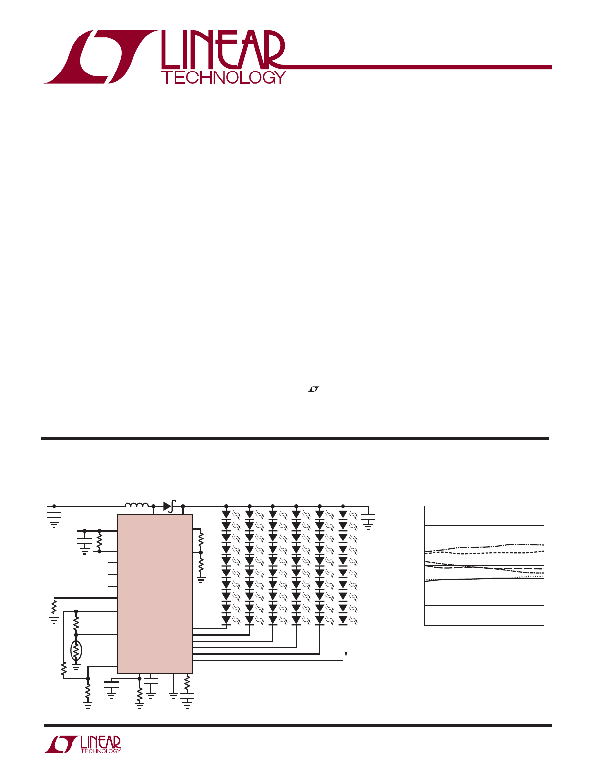
TYPICAL APPLICATION
90% Effi cient LED Driver for 60 White LEDs
PV
IN
8V TO 40V
2.2μF
2.2μF
51.1k
60.4k
V
IN
5V
SHDN
PWM
SYNC
10k
100k
100k
100k
10μH
V
IN
OPENLED
SHDN
PWM
SYNC
RT
V
REF
CTRL
T
SETISET
47pF
14.7k
SW
LT3598
SS GND
10nF
V
V
OUT
O_SW
LED1
LED2
LED3
LED4
LED5
LED6
FB
V
C
2.61k
15nF
1.00M
30.9k
3598 TA01a
20mA
4.7μ
1.5
ALL SIX LED STRINGS
1.0
0.5
0
MATCHING (%)
–0.5
–1.0
–1.5
–50
LED Current Matching
050
–25
25 75 100 125
TEMPERATURE (°C)
3598 TA01b
3598f
1
Page 2
LT3598
(Note 1)
SHDN ................................................................VIN + 3V
, OPENLED ...........................................................30V
V
IN
SW Voltage ...............................................................45V
, V
V
OUT
LED1 to LED6 ............................................................44V
PWM, SYNC, CTRL, RT, SS, V
, FB Voltage..........................................................6V
V
REF
, T
I
SET
Operating Junction Temperature Range
(Note 2) .................................................. –40°C to 125°C
Maximum Junction Temperature........................... 125°C
Storage Temperature Range ................... –65°C to 150°C
Voltage .................................................44V
O_SW
...................................6V
C
.....................................................................6V
SET
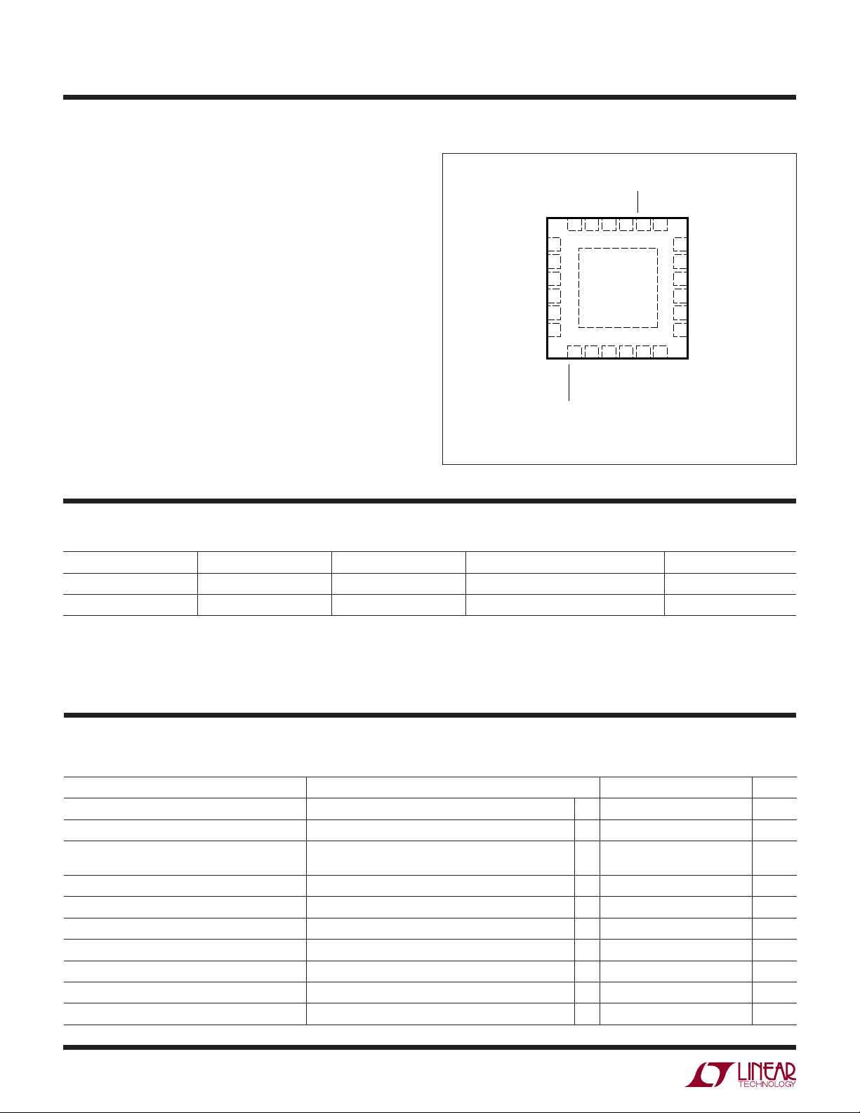
PIN CONFIGURATION ABSOLUTE MAXIMUM RATINGS
TOP VIEW
O_SWVOUT
V
SW
VINSHDN
GND
24 23 22 21 20 19
LED1
1
LED2
2
LED3
3
LED4
4
LED5
5
LED6
6
24-LEAD (4mm × 4mm) PLASTIC QFN
T
EXPOSED PAD (PIN 25) IS GND, MUST BE SOLDERED TO PCB
JMAX
25
7 8 9
OPENLED
10 11 12
C
V
SET
I
CTRL
UF PACKAGE
= 125°C, θJA = 37°C/W
18
V
REF
SS
17
RT
16
PWM
15
SYNC
14
13
NC
FB
SET
T
ORDER INFORMATION
LEAD FREE FINISH TAPE AND REEL PART MARKING* PACKAGE DESCRIPTION TEMPERATURE RANGE
LT3598EUF#PBF LT3598EUF#TRPBF 3598
LT3598IUF#PBF LT3598IUF#TRPBF 3598
Consult LTC Marketing for parts specifi ed with wider operating temperature ranges. *The temperature grade is identifi ed by a label on the shipping container.
Consult LTC Marketing for information on non-standard lead based fi nish parts.
For more information on lead free part marking, go to:
For more information on tape and reel specifi cations, go to:
ELECTRICAL CHARACTERISTICS
The l denotes the specifi cations which apply over the full operating
http://www.linear.com/leadfree/
http://www.linear.com/tapeandreel/
temperature range, otherwise specifi cations are at TA = 25°C. VIN = 5V, V
PARAMETER CONDITIONS MIN TYP MAX UNITS
Minimum Operating Voltage 3 3.2 V
Maximum Operating Voltage 30 V
Reference Voltage
Reference Voltage Line Regulation 3 < VIN < 30V, VC = 0.3V 0.01 0.03 %/V
Maximum V
FB Pin Bias Current V
FB Error Amp Transconductance ΔI = 5μA 300 μmhos
FB Error Amp Voltage Gain 600 V/V
FB Pin Voltage 1.22 1.24 1.26 V
Current Loop Amp Transconductance 21 μmhos
Pin Current Out of Pin 200 μA
REF
= 1.230V (Note 3) 100 250 nA
FB
24-Lead (4mm × 4mm) Plastic QFN
24-Lead (4mm × 4mm) Plastic QFN
= VIN unless otherwise noted. (Note 2)
SHDN
1.216
l
1.210
–40°C to 125°C
–40°C to 125°C
1.230 1.260
1.260
3598f
V
V
2
Page 3

LT3598
ELECTRICAL CHARACTERISTICS
The l denotes the specifi cations which apply over the full operating
temperature range, otherwise specifi cations are at T
= 25°C. VIN = 5V, V
A
PARAMETER CONDITIONS MIN TYP MAX UNITS
Current Loop Amp Voltage Gain 80 V/V
Sink Current 10 μA
V
C
Quiescent Current V
Quiescent Current in Shutdown V
Voltage V
I
SET
LED Current R
= 5V, PWM = 0V, Not Switching 3.5 5 mA
SHDN
= 0V 0 1 μA
SHDN
= 1.5V, V
CTRL
= 14.7kΩ 19.5 20 20.7 mA
ISET
TSET
= 1.5V, R
LED String Current Matching 20mA LED Current
LED Open Detection Threshold 0.2 0.25 V
OPENLED Sink Current 2mA
Minimum LED Regulation Voltage 0.8 V
LED1-6 Leakage Current V
CTRL Pin Bias Current V
= 1V, V
LED1-6
V
= 42V, V
LED1-6
= 0.8V (Note 4) 50 125 nA
CTRL
= 5V, PWM = 0V
OUT
= 44V, PWM = 0V
OUT
Switching Frequency RT = 309kΩ
RT = 51.1kΩ
RT = 14.7kΩ
T
Voltage 602 mV
SET
Maximum Switch Duty Cycle RT = 309kΩ
RT = 51.1kΩ
RT = 14.7kΩ
Switch Current Limit (Note 5) 1.5 2 2.5 A
Switch V
CESAT
Switch Leakage Current V
SHDN Pin Current V
ISW = 0.5A 0.12 V
= 40V 0.2 5 μA
SW
V
SHDN
SHDN
= 0V, V
= 5V, V
IN
IN
= 0V
= 5V
SHDN Voltage High 1.6 V
SHDN Voltage Low 0.4 V
Soft-Start Charging Current V
= 0.1V 5 10 15 μA
SS
PWM Input High Voltage 1V
PWM Input Low Voltage 0.4 V
PWM Pin Bias Current PWM = 3.3V 0.1 1 μA
SYNC Input High Voltage 1.5 V
SYNC Input Low Voltage 0.4 V
SYNC Pin Bias Current SYNC = 0V
SYNC = 3.3V
V
Switch Resistance 1000 Ω
O_SW
Note 1: Stresses beyond those listed under Absolute Maximum Ratings
may cause permanent damage to the device. Exposure to any Absolute
Maximum Rating condition for extended periods may affect device
reliability and lifetime.
Note 2: The LT3598E is guaranteed to meet performance specifi cations
from 0°C to 125°C junction temperature. Specifi cations over the –40°C
to 125°C operating junction temperature range are assured by design,
= VIN unless otherwise noted. (Note 2)
SHDN
= 14.7kΩ 0.985 1.000 1.015 V
ISET
l
171
0.9
2.25
90
l
87
80
±0.5 ±1.5 %
0.1
0.2
190
1
2.5
1
2
209
1.1
2.75
μA
μA
kHz
MHz
MHz
95
90
86
0.1
30
25
0.1
60
50
1
μA
μA
μA
1
μA
%
%
%
characterization and correlation with statistical process controls. The
LT3598I is guaranteed over the full –40°C to 125°C operating junction
temperature range.
Note 3: Current fl ows out of FB pin.
Note 4: Current fl ows out of CTRL pin.
Note 5: Current limit guaranteed by design and/or correlation to static test.
Current limit is independent of duty cycle and is guaranteed by design.
3598f
3
Page 4

LT3598
TYPICAL PERFORMANCE CHARACTERISTICS
SHDN Pin Turn-On Threshold SHDN Pin Current Quiescent Current
1.5
1.4
1.3
SHDN THRESHOLD (V)
1.2
–50
050
–25
25 75 100 125
TEMPERATURE (°C)
3598 G01
Reference Voltage Oscillator Frequency Current Limit
1.240
1.235
50
45
–50°C
40
35
30
25
20
15
SHDN PIN CURRENT (μA)
10
5
0
0
5
3.0
2.5
25°C
20
15
10
V
SHDN
2.5MHz
25
(V)
125°C
30
3598 G02
6
5
4
3
QUIESCENT CURRENT (mA)
2
35
–50
2.8
2.4
050
–25
25 75 100 125
TEMPERATURE (°C)
3598 G03
1.230
1.225
REFERENCE VOLTAGE (V)
1.220
1.215
0.40
0.35
0.30
0.25
(V)
0.20
CESAT
V
0.15
0.10
0.05
VIN = 40V
VIN = 5V
050
–50
–25
V
CESAT
0
0.25 0.750.50 1.00 1.25 1.5O
0
25 75 100 125
TEMPERATURE (°C)
125°C
–50°C
SWITCH CURRENT (A)
VIN = 30V
3598 G04
25°C
3598 G07
2.0
1.5
1.0
OSCILLATOR FREQUENCY (MHz)
0.5
0
–50
050
–25
TEMPERATURE (°C)
1MHz
200kHz
25 75 100 125
3598 G05
2.0
1.6
CURRENT (A)
1.2
0.8
0.4
–50
–25
Soft-Start Pin Current Feedback Pin Voltage
15.0
12.5
(μA)
10.0
SS
I
7.5
5.0
–50
050
–25
25 75 100 125
TEMPERATURE (°C)
3598 G08
1.24
1.23
1.22
FEEDBACK VOLTAGE (V)
1.21
1.20
–50
VC = 1.5V
VC = 1V
–25
050
25 75 100 125
TEMPERATURE (°C)
050
25 75 100 125
TEMPERATURE (°C)
3598 G06
3598 G09
4
3598f
Page 5
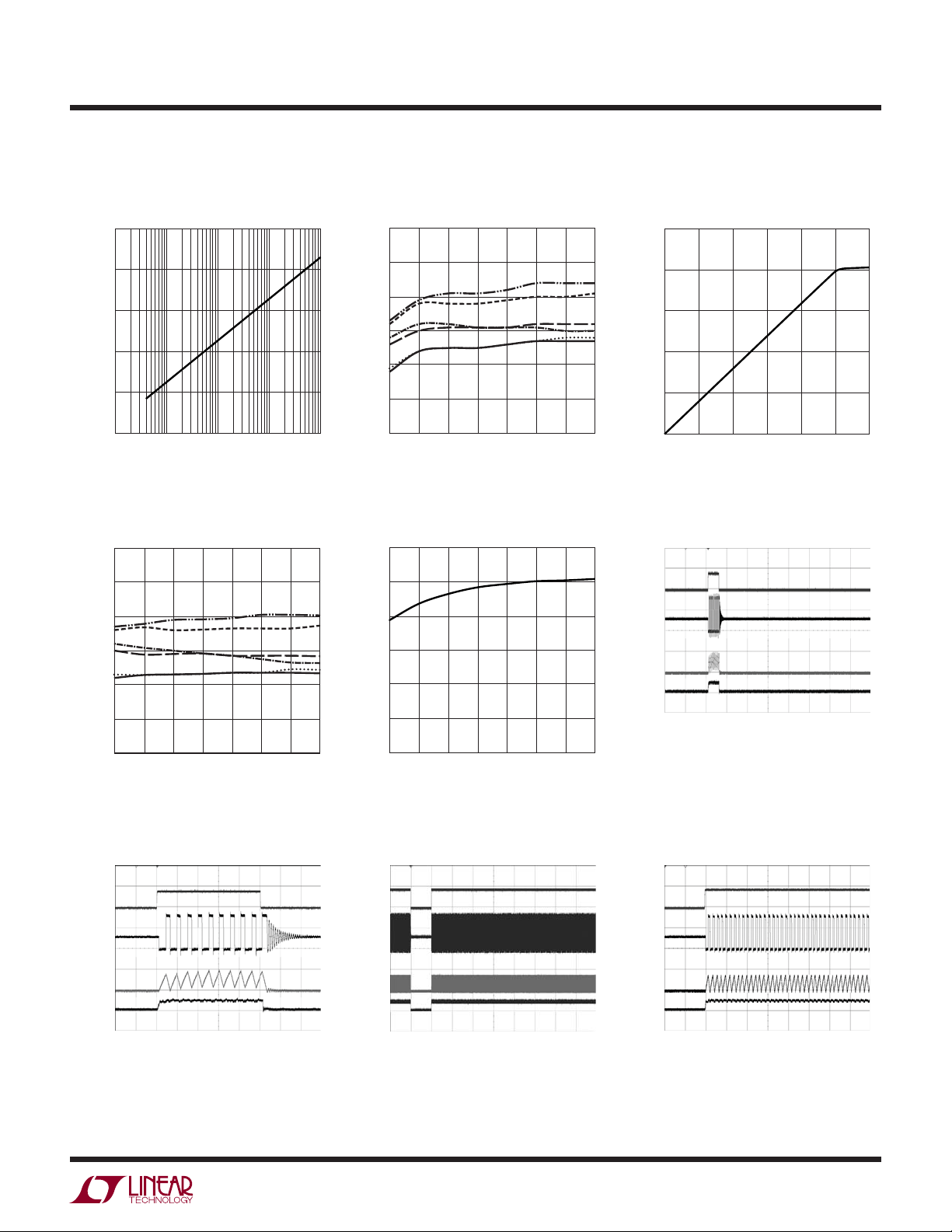
TYPICAL PERFORMANCE CHARACTERISTICS
LED Current vs PWM Duty Cycle LED Current vs Temperature LED Current vs CTRL Voltage
100
20.3
25
LT3598
10
1
0.1
LED CURRENT (mA)
0.01
0.001
0.01
PWM DUTY CYCLE (%)
1100.1 100
3598 G10
20.2
20.1
20.0
19.9
LED CURRENT (mA)
19.8
19.7
–25
–50
LED Current vs Temperature OPENLED Sink Current
1.5
1.0
0.5
0.0
MATCHING (%)
–0.5
–1.0
–1.5
–50
050
–25
25 75 100 125
TEMPERATURE (°C)
3598 G13
3.0
2.5
2.0
1.5
1.0
OPENLED CURRENT (mA)
0.5
0
–50
–25
050
25 75 100 125
TEMPERATURE (°C)
050
25 75 100 125
TEMPERATURE (°C)
3598 G11
3598 G14
20
15
10
LED CURRENT (mA)
5
0
0
LED Current Waveforms
(0.1% PWM)
PWM
5V/DIV
SW
20V/DIV
I
L
1A/DIV
I
LED1
50mA/DIV
0.2 0.4
CTRL VOLTAGE (V)
0.6
20μs/DIV
0.8
1.0
1.2
3598 G12
3598 G15
PWM
5V/DIV
SW
20V/DIV
1A/DIV
I
LED1
50mA/DIV
LED Current Waveforms
(0.1% PWM)
I
L
2μs/DIV
3598 G16
PWM
5V/DIV
SW
20V/DIV
1A/DIV
I
LED1
50mA/DIV
LED Current Waveforms
(90% PWM)
I
L
100μs/DIV
3598 G17
PWM
5V/DIV
SW
20V/DIV
1A/DIV
I
LED1
50mA/DIV
LED Current Waveforms
(90% PWM)
I
L
5μs/DIV
3598 G18
3598f
5
Page 6

LT3598
PIN FUNCTIONS
LED1-6 (Pins 1, 2, 3, 4, 5, 6): LED String Output. Connect
the bottom cathode of each LED string to these pins. Tie
pins to V
if the string is not used.
OUT
OPENLED (Pin 7): Open LED Flag When Any LED String
Opens. The output is open-collector. Tie a resistor to other
supply for open LED fl ag function.
(Pin 8): Programs LED Current for Each String. Con-
I
SET
nect a 14.7k resistor between I
and GND to program
SET
each LED string current to 20mA. A 47pF capacitor on the
pin reduces current ripple in each LED string.
I
SET
CTRL (Pin 9): LED Current Control. If the CTRL pin is not
used, tie this pin to V
(Pin 10): Error Amplifi er Output Pin. Tie the external
V
C
through a 10k to 20k resistor.
REF
compensation network to this pin.
FB (Pin 11): Feedback Pin for Overvoltage Protection.
Reference voltage is 1.230V. Connect the resistive divider
tap here. Minimize trace area at FB. Set V
to V
= 1.230(1 + R2/R1) when overvoltage protection
OUT
according
OUT
occurs (see Figure 2).
T
(Pin 12): An external resistor divider from V
SET
REF
programs a decrease in LED current versus internal junction
temperature (setting temperature breakpoint and slope).
If the T
pin is not used, tie this pin to V
SET
REF
.
NC (Pin 13): No Connection.
SYNC (Pin 14): Frequency Synchronization Pin. This
input allows for synchronizing the operating frequency
to an external clock. The RT resistor should be chosen to
program a switching frequency 20% slower than SYNC
pulse frequency. This pin should be grounded if this
feature is not used.
PWM (Pin 15): Input Pin for PWM Dimming Control. Above
1V allows converter switching and below 1V disables
switching with VC pin level maintained. A PWM signal
driving the PWM pin provides accurate dimming control.
The PWM signal can be driven from 0V to 5V. If unused,
the pin should be connected to V
REF
.
RT (Pin 16): A resistor to ground programs switching
frequency between 200kHz and 2.5MHz. For SYNC function, choose the resistor to program a frequency 20%
slower than the SYNC pulse frequency. Do not leave this
pin open.
SS (Pin 17): Soft-Start Pin. Place a soft-start capacitor
here. Upon start-up, a 10μA current charges the capacitor.
Use a larger capacitor for slower start-up. Leave open if
not used.
V
(Pin 18): Bandgap Voltage Reference. Internally set
REF
to 1.230V. This pin can supply up to 100μA. Can be used
to program the CTRL pin voltage using resistor dividers
to ground.
GND (Pin 19): Ground. Tie directly to local ground
plane.
SHDN (Pin 20): Shutdown Pin. Tie to 1.6V or more to en-
able the device. Tie below 0.4V or less to disable device.
Do not fl oat this pin.
V
(Pin 21): Input Supply Pin. Must be locally bypassed
IN
with a capacitor to ground.
SW (Pin 22): Switch Pin. This is the collector of the in-
ternal NPN power switch. Minimize the metal trace area
connected to this pin to minimize EMI.
V
(Pin 23): Output Pin. This pin provides power to
OUT
all LEDs.
V
(Pin 24): Drain of an Internal PMOS. The internal
O_SW
PMOS disconnects the feedback resistors from the V
OUT
pin during shutdown and the PWM transitioned to low.
Exposed Pad (Pin 25): Ground. The Exposed Pad must
be soldered to the PCB.
6
3598f
Page 7

BLOCK DIAGRAM
LT3598
10
17
15
18
9
V
C
SS
PWM
V
REF
CTRL
20
SHDN
1.230V
21
V
IN
REF
PWM DIMMING
LOGIC
SLOPE
16
OSCILLATOR
3
14
RT
SYNC
+
A2
–
S
R
Q
22
SW
Q1
+
OVP g
LED g
A3
–
+
m
–
0.8V
+
m
V
GND
GND
V
OUT
O_SW
19
25
23
24
FB
11
–
OPENLED DETECTION
OPENLED
7
T
SET
12
–
A1
V
PTAT
+
LED
DRIVE
CIRCUITRY
I
SET
8
DISABLE
DETECTION
LED1
V
OUT
LED
LED2
LED3
LED4
LED5
LED6
3598 F01
1
2
3
4
5
6
Figure 1. Block Diagram
3598f
7
Page 8

LT3598
OPERATION
The LT3598 uses a constant-frequency, peak current mode
control scheme to provide excellent line and load regulation.
Each string can drive up to 30mA with 1.5% matching accuracy between strings. Operation can be best understood
by referring to the Block Diagram in Figure 1.
LT3598 has a built-in boost converter which converts the
input voltage to a higher output voltage to drive LEDs.
The LED strings are connected to current sources where
the current level is set with an external resistor on the
pin. The LED1 to LED6 voltages are monitored for
I
SET
output voltage regulation. During normal operation, when
all LEDs are used, the lowest LED pin voltage (LED1 to
LED6) is used to regulate the output voltage to ensure all
LED strings have enough voltage to run the programmed
current.
For any unused LED strings, tie their LED pins to V
OUT
.
An unused LED string is no longer in the regulation loop,
nor does it affect open LED detection. Never allow unused
LED strings to be left open.
The basic loop uses a pulse from an internal oscillator
to set the SR latch and turn on the internal power NPN
switch Q1. The signal at the noninverting input of the PWM
comparator (A2 slope) is proportional to the sum of the
switch current and oscillator ramp. When slope exceeds
(the output of the gm amplifi er), the PWM comparator
V
C
resets the latch. The switch is then turned off, causing the
inductor current to lift the SW pin and turn on an external
Schottky diode connected to the output. Inductor current
fl ows via the Schottky diode charging the output capacitor. The switch is turned on again at the next reset cycle
of the internal oscillator. During normal operation, the V
C
voltage controls the peak switch current limit and, hence,
the inductor current available to the output LEDs.
Dimming of the LEDs is accomplished by pulsing the LED
current using the PWM pin. When the PWM pin is low,
switching is disabled and the error amplifi er is turned off
so that it does not drive the V
on the V
pin are disabled so that the state of the VC pin
C
pin. Also, all internal loads
C
is maintained on the external compensation capacitor.
This feature reduces transient recovery time. When the
PWM input again transitions high, the peak switch current
returns to the correct value.
The LT3598 uses the FB pin to provide overvoltage protection when all LED strings are open. There is an internal
PMOS switch between V
OUT
and V
that is controlled
O_SW
by the PWM signal. During the PWM off-period, this
PMOS is turned off, allowing for higher dimming range
and lower current during shutdown. A resistor divider is
connected between the V
pin and ground, which sets
O_SW
the overvoltage protection voltage.
If the LED1-6 pin voltage is below 0.2V (for a certain delay
after 80% of the programmed output voltage is reached),
the string is treated as an open LED string. As a result,
OPENLED lag is set. If a LED string is open in the middle
of the operation, the regulation will continue.
OPENLED detection is disabled during the start-up phase
to avoid erratic fl ag generation. An LED string that is disabled by connecting its LED pin to V
is not an open
OUT
LED condition. During normal operation, if an LED string is
open and has the lowest LED pin voltage, the output voltage will regulate itself to fi nd another LED string that has
the lowest LED pin voltage at about 0.8V. If the open LED
string has an LED voltage above 0.8V, the output voltage
will remain the same. When the LED string is open, it is
no longer in the regulation loop. The OPENLED detection
is active only when the PWM signal is enabled. To avoid
spurious OPENLED detection and high PWM dimming
ratio, more output capacitance is recommended to allow
less voltage drop on V
OUT
.
During start-up, 10μA of current charges the external
soft-start capacitor. The SS pin directly limits the rate
of voltage rise on the V
pin, which in turn, limits the
C
peak switch current. Soft-start also enables the switching frequency foldback to provide a clean start-up for
the LT3598. Current limit protects the power switch and
external components.
8
3598f
Page 9

APPLICATIONS INFORMATION
LT3598
Inductor Selection
Table 1 lists several inductors that work well with the
LT3598, however, there are many other manufacturers and
devices that can be used. Consult each manufacturer for
detailed information on their entire range of parts. Ferrite
core inductors should be used to obtain the best effi ciency.
Choose an inductor that can handle the necessary peak
current without saturating. Also, ensure that the inductor
2
has a low DCR (copper wire resistance) to minimize I
R
power losses. Values between 4.7μH and 22μH will suffi ce
for most applications.
Inductor manufacturers specify the maximum current
rating as the current where inductance falls by a given
percentage of its nominal value. An inductor can pass a
current greater than its rated value without damaging it.
Consult each manufacturer to determine how the maximum
inductor current is measured and how much more current
the inductor can reliably conduct.
Table 1. Recommended Inductors
MAX
DCR
(Ω)
0.07
0.06
0.12
0.055
0.065
0.12
0.065
0.083
0.038
CURRENT
RATING
(A) VENDOR
2.2
2.26
1.90
2.45
2.10
2.00
TOKO
www.toko.com
2.2
Würth Electronics
2
www.we-online.com
1.7
Sumida
www.sumida.com
www.vishay.com
www.cooperet.com
www.coilcraft.com
PART
B1015AS-100M
#817FY-4R7M
1123AS-4R7M
74454068
74454010
7447745100
CDH74NP-120L
CDH74NP-150L
CDRH6D38-100
IHLP-2525BD-01 10 0.129 2.5 Vishay
SD25-4R7-R 4.7 0.056 1.83 Cooper
LPS4018-472ML 4.7 0.200 1.8 Coilcraft
L
(μH)
10
4.7
4.7
6.8
10
10
12
15
10
Capacitor Selection
Low ESR (equivalent series resistance) ceramic capacitors should be used at the output to minimize the output
ripple voltage. Use only X5R or X7R dielectrics, as these
materials retain their capacitance over wider voltage and
temperature ranges than other dielectrics. A 4.7μF to 10μF
output capacitor is suffi cient for most high output current
designs. Table 2 lists some suggested manufacturers.
Consult the manufacturers for detailed information on
their entire selection of ceramic parts.
Table 2. Recommended Ceramic Capacitor Manufacturers
Taiyo Yuden 408-573-4150
AVX 843-448-9411
Murata 770-436-1300
Kemet 408-986-0424
United Chemi-Con 847-696-2000
www.t-yuden.com
www.avxcorp.com
www.murata.com
www.kemet.com
www.chemi-con.com
Diode Selection
Schottky diodes, with their low forward voltage drop and
fast switching speed, must be used for all LT3598 applications. Do not use P-N diodes. Table 3 lists several Schottky
diodes that work well. The diode’s average current rating
must exceed the application’s average output current.
The diode’s maximum reverse voltage must exceed the
application’s output voltage. A 2A diode is suffi cient for
most designs. For PWM dimming applications, be aware
of the reverse leakage current of the diode. Lower leakage
current will drain the output capacitor less, allowing for
higher dimming range. The companies below offer Schottky
diodes with high voltage and current ratings.
Table 3. Suggested Diodes
MAX
CURRENT
PART
B250A
B240A
SBR140S3
SBM340, PDS340
HSM150G
HSM150J
SS3H9 3 90 Vishay
(A)
2
2
1
3
1
1
MAX REVERSE
VOLTAGE
(V) MANUFACTURER
50
40
40
40
50
50
Diodes, Inc.
www.diodes.com
Microsemi
www.microsemi.com
www.vishay.com
3598f
9
Page 10
LT3598
APPLICATIONS INFORMATION
Overvoltage Protection
The LT3598 uses the FB pin to provide regulated overvoltage
protection when all LED strings are open. A resistor divider
is connected between the V
2). There is an internal PMOS switch between V
, which is controlled by the PWM signal. The PMOS
V
O_SW
pin and ground (Figure
O_SW
OUT
and
switch addition prevents the feedback resistor divider from
draining the output capacitor during PWM off-period, allowing for a higher dimming range without falsely tripping
the OPENLED fl ag. It also reduces the system current in
shutdown. This PMOS has about 1k resistance, so select
FB resistors taking this resistance into account.
To set the maximum output voltage, select the values
of R1 and R2 (see Figure 2) according to the following
equation:
R
2
LT3598
⎛
⎜
⎝
VV
OUT MAX()
.=+
1 230 1
Figure 2. Overvoltage Protection
Voltage Feedback Connections
FB
3598 F02
⎞
⎟
⎠
R
1
V
OUT
V
O_SW
R2
R1
The output voltage should be set higher than the normal
LED string operating voltage. Under normal operation,
LED1 to LED6 pin voltages are monitored and provide
feedback information to the converter for output voltage regulation given the programmed LED current. The
maximum output regulation loop is activated only when
all LEDs are open.
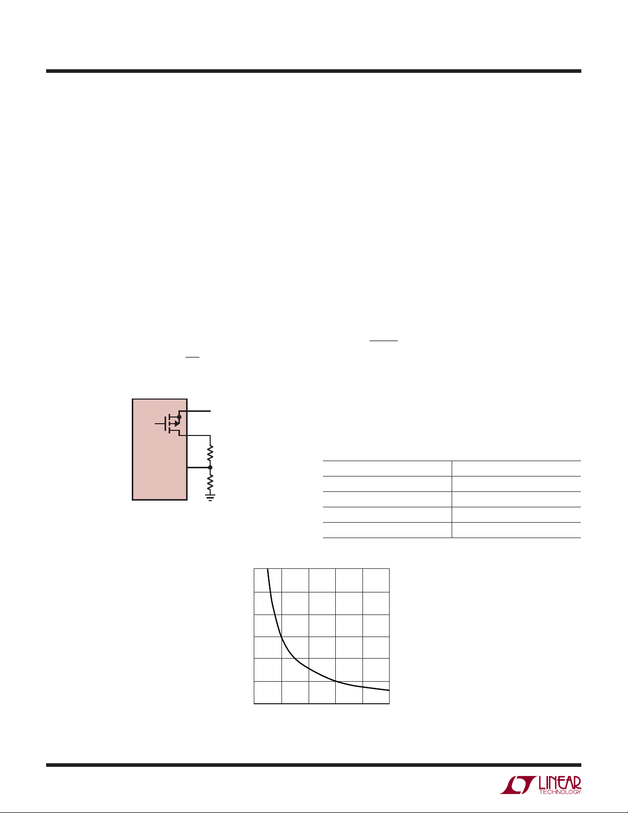
Programming Maximum LED Current
Maximum LED current is programmed by placing a resistor between the I
pin and ground (R
SET
ISET
). The I
SET
pin
resistor can be selected from 10k to 100k.
The LED current is programmed according to the follow-
ing equation:
V
LED
≈
294
R
ISET
I
See Table 4 and Figure 3 for resistor values and corresponding programmed LED current.
LED current can also be adjusted by programming the
CTRL pin voltage.
Table 4. R
Value Selection for LED Current
ISET
LED CURRENT (mA) RESISTOR ON I
3mA 97.6
10mA 29.4
20mA 14.7
30mA 9.76
SET
PIN (k)
10
30
25
20
15
10
LED CURRENT (mA)
5
0
0
Figure 3. R
40 80
20
Value Selection for LED Current
ISET
60 100
R
(k)
ISET
3598 F03
3598f
Page 11
APPLICATIONS INFORMATION
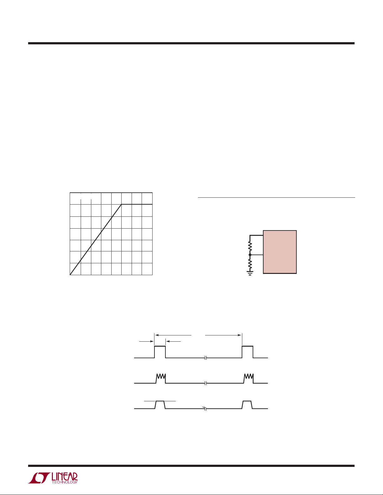
LED Current Dimming
Two different types of dimming control can be used with
the LT3598. The LED current can be set by modulating
the CTRL pin or the PWM pin.
For some applications, a variable DC voltage that adjusts
the LED current is the preferred method of brightness
control. The CTRL pin voltage can be modulated to set
the dimming of the LED string (see Figures 4 and 5). As
the voltage on the CTRL pin increases from 0V to 1.0V,
the LED current increases from 0 to the programmed LED
current level. As the CTRL pin voltage increases beyond
1V, it has no effect on the LED current.
35
R
= 9.76k
ISET
30
25
LT3598
TM
For True Color PWM
to a 3000:1 PWM dimming range. This is achieved by
allowing the duty cycle of the PWM pin (connected to
the IC and an internal switch in series with the LED(s)),
to be reduced from 100% to as low as 0.1% for a PWM
frequency of 100Hz (Figure 6). PWM duty cycle dimming
allows for constant LED color to be maintained over the
entire dimming range.
For wide PWM dimming range, higher switching frequency
and lower PWM frequency confi guration are needed. Special considerations are required for component selection
and compensation network. Please contact factory for
optimized components selection if very high dimming
ratio is desired.
True Color PWM is a registered trademark of Linear Technology Corporation.
dimming, the LT3598 provides up
20
V
15
LED CURRENT (mA)
10
5
0
0.2
0
0.4 0.8
0.6 1 1.2 1.6
CTRL (V)
1.4
3598 F04
REF
R2
R1
LT3598
CTRL
3598 F05
Figure 4. LED Current vs CTRL Voltage Figure 5. LED Current vs CTRL
T
PWM
(= 1/f
)
PWM
3598 F06
PWM
INDUCTOR
CURRENT
LED
CURRENT
TON
MAX I
PWM
LED
Figure 6. LED Current Using PWM Dimming
3598f
11
Page 12
LT3598
APPLICATIONS INFORMATION
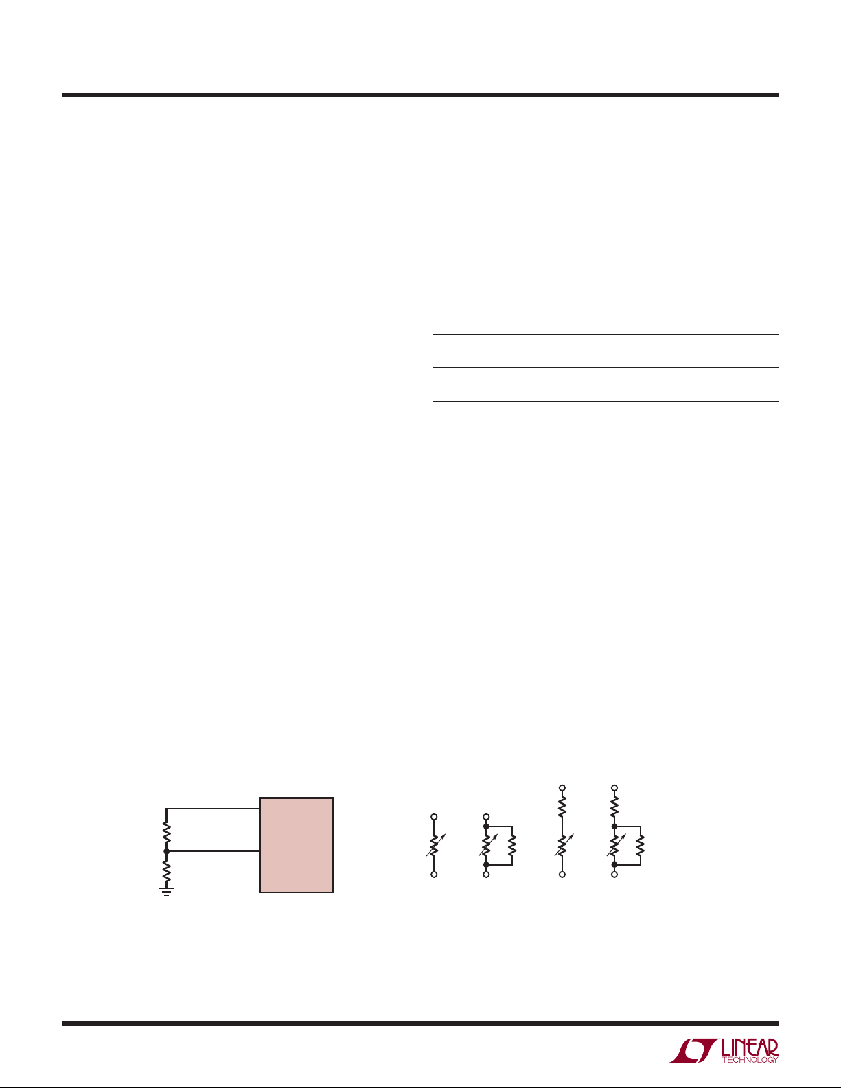
LED Current Derating Using the CTRL Pin
A useful feature of the LT3598 is its ability to program a
derating curve for maximum LED current versus temperature. LED data sheets provide curves of maximum-allowable
LED current versus temperature to warn against exceeding this current limit and damaging the LED. The LT3598
allows the output LEDs to be programmed for maximum
allowable current while still protecting the LEDs from
excessive currents at high temperature. This is achieved
by programming a voltage at the CTRL pin with a negative temperature coeffi cient using a resistor divider with
temperature dependent resistance (Figure 7). As ambient
temperature increases, the CTRL voltage will fall below the
internal 1V voltage reference, causing LED currents to be
controlled by the CTRL pin voltage. The LED current curve
breakpoint and slope versus temperature is defi ned by the
choice of resistor ratios and use of temperature-dependent
resistance in the divider for the CTRL pin.
Table 5 shows a list of manufacturers/distributors of NTC
resistors. There are several other manufacturers available and the chosen supplier should be contacted for
more detailed information. If an NTC resistor is used to
indicate LED temperature, it is effective only if the resistor
is connected as closely as possible to the LED strings.
LED derating curves shown by manufacturers are listed
for ambient temperature. The NTC resistor should have
the same ambient temperature as the LEDs. Since the
temperature dependency of an NTC resistor can be nonlinear over a wide range of temperatures, it is important
to obtain a resistor’s exact value over temperature from
the manufacturer. Hand calculations of CTRL voltage can
then be performed at each given temperature, resulting
in the CTRL versus temperature plotted curve. Several
iterations of resistor value calculations may be required
to achieve the desired breakpoint and slope of the LED
current derating curve.
Table 5. NTC Resistor Manufacturers/Distributors
Murata Electronics North America 770-436-1300
TDK Corporation 516-535-2600
Digi-Key 800-344-4539
www.murata.com
www.tdk.com
www.digikey.com
If calculating the CTRL voltage at various temperatures
gives a downward slope that is too strong, alternative
resistor networks can be chosen (B, C, D in Figure 7)
which use temperature independent resistance to reduce
the effects of the NTC resistor overtemperature.
Murata Electronics provides a selection of NTC resistors
with complete data over a wide range of temperatures.
In addition, a software tool is available which allows the
user to select from different resistor networks and NTC
resistor values, and then simulate the exact output voltage curve (CTRL behavior) overtemperature. Referred
to as the “Murata Chip NTC Thermistor Output Voltage
Simulator,” users can log onto www.murata.com and
download the software followed by instructions for creating an output voltage V
supply (V
REF
).
(CTRL) from a specifi ed VCC
OUT
12
R2
R1
(OPTION A TO D)
R
V
REF
LT3598
CTRL
Figure 7 . LED Current Derating vs Temperature Using NTC Resistor
R
NTC
R
NTC
R
X
Y
R
NTC
R
NTC
DCBA
R
Y
3598 F07
R
X
3598f
Page 13
APPLICATIONS INFORMATION
LT3598
Using the T
Pin for Thermal Protection
SET
The LT3598 contains a special programmable thermal
regulation loop that limits the internal junction temperature
of the part. Since the LT3598 topology consists of a single
boost converter with six linear current sources, any LED
string voltage mismatch will cause additional power to be
dissipated in the package. This topology provides excellent
current matching between LED strings and allows a single
power stage to drive a large number of LEDs, but at the
price of additional power dissipation inside the part (which
means a higher junction temperature). Being able to limit
the maximum junction temperature allows the benefi ts of
this topology to be fully realized. This thermal regulation
feature provides important protection at high ambient temperatures, and allows a given application to be optimized
for typical, not worst-case, ambient temperatures with the
assurance that the LT3598 will automatically protect itself
and the LED strings under worst-case conditions.
The operation of the thermal loop is simple. As the ambient temperature increases, so does the internal junction
temperature of the part. Once the programmed maximum
junction temperature is reached, the LT3598 begins to
linearly reduce the LED current, as needed, to try and
maintain this temperature. This can only be achieved
when the ambient temperature stays below the desired
maximum junction temperature. If the ambient temperature continues to rise past the programmed maximum
junction temperature, the LEDs current will be reduced
to approximately 5% of the full LED current.
While this feature is intended to directly protect the LT3598,
it can also be used to derate the LED current at high temperatures. Since there is a direct relationship between the
LED temperature and LT3598 junction temperature, the
TSET function also provides some LED current derating
at high temperatures.
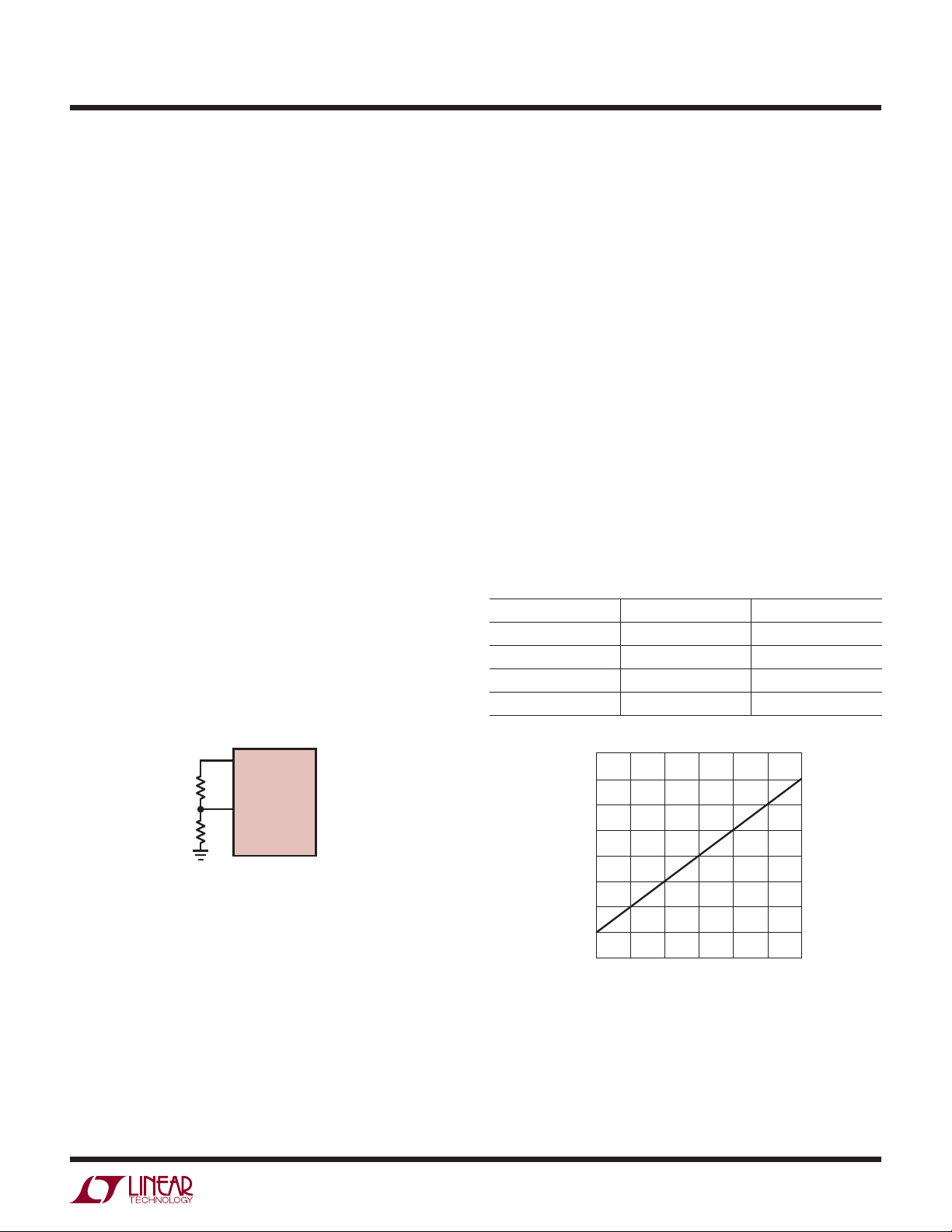
Two external resistors program the maximum IC junction
temperature using a resistor divider from the V
REF
pin, as
shown in Figure 8. Choose the ratio of R1 and R2 for the
desired junction temperature. Figure 9 shows the relationship of T
voltage to junction temperature, and Table 6
SET
shows commonly used values for R1 and R2.
Table 6. T
Junction Temperature
SET
TJ (°C) R1 R2
90 100k 67.7k
100 100k 63.3k
110 100k 59k
120 100k 54.9k
V
REF
R2
R1
Figure 8. Programming the T
LT3598
T
SET
3598 F08
SET
Pin
900
850
800
750
700
THRESHOLD (mV)
650
TSET
V
600
550
500
25
0
JUNCTION TEMPERATURE (°C)
Figure 9. T
50
75
Pin Threshold
SET
100 125
150
3598 F09
3598f
13
Page 14

LT3598
APPLICATIONS INFORMATION
Programming Switching Frequency
The switching frequency of the LT3598 should be programmed between 200kHz and 2.5MHz by an external
resistor connected between the RT pin and ground. Do not
leave this pin open. See Table 7 and Figure 10 for resistor
values and corresponding frequencies.
Selecting the optimum switching frequency depends
on several factors. Inductor size is reduced with higher
frequency, but effi ciency drops slightly due to higher
switching losses. In addition, some applications require
very high duty cycles to drive a large number of LEDs from
a low supply. Low switching frequency allows a greater
operational duty cycle and, hence, a greater number of
LEDs to be driven. In each case, the switching frequency
can be tailored to provide the optimum solution. When
programming the switching frequency, the total power
losses within the IC should be considered.
Table 7. Switching Frequency
SWITCHING FREQUENCY (MHz) RT (k)
2.5 14.7
2 20.5
1.5 29.4
1 51.1
0.5 105
0.2 301
Switching Frequency Synchronization
The nominal operating frequency of the LT3598 is programmed using a resistor from the RT pin to ground
and can be controlled over a 200kHz to 2.5MHz range. In
addition, the internal oscillator can be synchronized to an
external clock applied to the SYNC pin. The synchronizing
clock signal input to the LT3598 must have a frequency
between 240kHz and 3MHz, a duty cycle between 20%
and 80%, a low state below 0.4V and a high state above
1.5V. Synchronization signals outside of these parameters
will cause erratic switching behavior. For proper operation,
an RT resistor should be chosen to program a switching
frequency 20% slower than the SYNC pulse frequency.
Synchronization occurs at a fi xed delay after the rising
edge of SYNC.
The SYNC pin should be grounded if the clock synchronization feature is not used. When the SYNC pin is grounded,
the internal oscillator generates switching frequency to
the converter.
Soft-Start and Switching Frequency Foldback
For many applications, it is necessary to minimize the
inrush current at start-up. The LT3598’s soft-start circuit
signifi cantly reduces the start-up current spike and output
voltage overshoot. Before the SS pin voltage reaches 1V,
the switching frequency will also fold back proportional
to the SS pin voltage. A typical value for the soft-start
capacitor is 10nF.
14
2.5
2.0
1.5
1.0
0.5
SWITCHING FREQUENCY (MHz)
0
10 100
Figure 10. Switching Frequency
RT (k)
1000
3598 F10
3598f
Page 15

APPLICATIONS INFORMATION
LT3598
OPENLED FLAG
The OPENLED pin is an open-collector output and needs
an external resistor tied to a supply (see Figure 11). If any
LED string is open during normal operation, the OPENLED
pin will be pulled down.
The OPENLED fl ag is only activated after the fi rst PWM
edge. The open LED detection is enabled only when the
PWM signal is enabled. There is a delay for OPENLED
fl ag generation when the PWM signal is enabled to avoid
generating a spurious fl ag signal. The maximum current
the OPENLED can sink is typically 2mA.
During start-up (see the Operation section), the open LED
detection is disabled. If an LED string is not used and tied
to V
, the string will not be in any fault detection.
OUT
LT3598
OPENLED
3598 F11
R1
chosen based on performance, size and cost. The compensation resistor and capacitor at V
are selected to optimize
C
control loop stability. For typical LED applications, a 15nF
compensation capacitor in series with a 3k resistor at V
C
is adequate.
Thermal Considerations
The LT3598 provides six channels for LED strings with
internal NPN devices serving as constant-current sources.
When LED strings are regulated, the lowest LED pin voltage
is typically 0.8V. The higher the programmed LED current,
the more power dissipation in the LT3598. For 30mA LED
programming current with a 100% PWM dimming ratio,
at least 144mW is dissipated within the IC due to current
sources. If the forward voltages of the six LED strings are
very dissimilar, there can be signifi cant power dissipation.
Thermal calculations shall include the power dissipation
on current sources in addition to conventional switch DC
loss, switch AC loss and input quiescent loss. For best
effi ciency, it is recommended that all channels have the
same number of LEDs, and each string has a similar voltage drop across the LEDs.
Figure 11. OPENLED Connection
Loop Compensation
The LT3598 has an internal transconductance error amplifi er for LED current regulation whose V
output compen-
C
sates the control loop. During an open LED event where
all LED strings are open, the V
node also compensates
C
the control loop. The external inductor, output capacitor,
and the compensation resistor and capacitor determine
the loop stability. The inductor and output capacitor are
Board Layout Considerations
As with all switching regulators, careful attention must be
paid to the PCB board layout and component placement.
To prevent electromagnetic interference (EMI) problems,
proper layout of high frequency switching paths is essential.
Minimize the length and area of all traces connected to the
switching node pin (SW). Always use a ground plane under
the switching regulator to minimize interplane coupling.
Good grounding is essential in LED fault detection.
3598f
15
Page 16

LT3598
TYPICAL APPLICATIONS
LED Driver for 40 White LEDs with Two Channels Unused
PV
IN
6V TO 40V
C1
2.2μF
C1: TAIYO YUDEN GMK325BJ225ML
C2: MURATA GRM32ER71H475K
C3: TAIYO YUDEN LMK212BJ225MG
D1: DIODES, INC. B240A
ÜRTH ELEKTRONIK 744777410
L1: W
: MURATA NCP18WF104J03RB
R
NTC
R8
60.4k
2.2μF
R1
51.1k
V
IN
5V
C3
SHDN
PWM
SYNC
R
HOT
10k
R
NTC
100k
R7
100k
R6
100k
IN
OPENLED
SHDN
PWM
SYNC
RT
V
REF
CTRL
T
SETISET
C5
47pF
L1
10μH
LT3598
R3
14.7k
D1
SWV
SS GND
C4
0.1μF
V
V
OUT
O_SW
LED1
LED2
LED3
LED4
LED5
LED6
C2
4.7μF
R4
1.00M
FB
R5
30.9k
20mA
V
C
R
C
2.61k
C
C
15nF
3598 TA02a
16
Effi ciency (PWM Dimming)
95
90
85
80
75
70
EFFICIENCY (%)
65
60
55
50
10 90
0
PVIN = 25V
PVIN = 12V
20 40
30 508060
TOTAL LED CURRENT (mA)
70
3598 TA02b
3598f
Page 17

TYPICAL APPLICATIONS
8
LED Driver for 30 White LEDs with 60mA Each String
LT3598
PV
IN
6V TO 40V
C1
2.2μF
C1: TAIYO YUDEN GMK325BJ225ML
C2: MURATA GRM32ER71H475KA88L
C3: TAIYO YUDEN LMK212BJ225MG
D1: VISHAY SS3H9
ÜRTH ELEKTRONIK 744777410
L1: W
: MURATA NCP18WF104J03RB
R
NTC
60.4k
R8
2.2μF
R1
51.1k
V
IN
5V
C3
R
10k
HOT
R
NTC
100k
R6
100k
SHDN
CTRL
PWM
SYNC
R7
100k
IN
OPENLED
SHDN
CTRL
PWM
SYNC
RT
V
REF
CTRL
T
SETISET
C5
47pF
L1
10μH
LT3598
R3
9.76k
D1
SWV
SS GND
C4
0.1μF
V
V
OUT
O_SW
LED1
LED2
LED3
LED4
LED5
LED6
C2
4.7μF
R4
1.00M
FB
R5
30.9k
60mA
V
C
R
C
2.61k
C
C
15nF
3598 TA03a
Effi ciency (PWM Dimming)
100
95
90
85
80
75
EFFICIENCY (%)
70
65
60
0
20 180
PVIN = 25V
PVIN = 12V
40 80
60 100
TOTAL LED CURRENT (mA)
120
140
160
3598 TA03b
Dimming Range (1000:1 PWM) at 125°C
Junction Temperature, 10ms Period
PWM
5V/DIV
SW
20V/DIV
I
LED1
100mA/DIV
2μs/DIV
359
3598f
17
Page 18

LT3598
TYPICAL APPLICATIONS
Auto Battery Powered Driver for 20 LEDs with 90mA Each String
PV
IN
6V TO 40V
2.2μF
C1: NIPPON CHEMI-CON KTS500B225M32NOTOO
C2: MURATA GRM32ER71H475KA88L
C3: TAIYO YUDEN LMK212BJ225MG
D1: VISHAY SS3H9
L1: W
V
R1
51.1k
IN
5V
2.2μF
C3
100k
SHDN
CTRL
PWM
R10
20k
R8
60.4k
R7
100k
C1
ÜRTH ELEKTRONIK 7447785004
IN
OPENLED
SHDN
CTRL
PWM
SYNC
RT
V
REF
CTRL
T
SETISET
C5
56pF
L1
4.7μH
LT3598
R3
9.76k
D1
SWV
SS GND
C4
0.1μF
V
V
OUT
O_SW
LED1
LED2
LED3
LED4
LED5
LED6
V
C2
4.7μF
R4
1.00M
FB
R5
30.9k
90mA
C
R
C
5.11k
C
C
6.8nF
3598 TA04a
95
90
85
80
75
EFFICIENCY (%)
70
65
60
20 180
0
Effi ciency
40 80
60 100
TOTAL LED CURRENT (mA)
120
140
160
3598 TA04b
Dimming Range 1000:1 PWM,
10ms Period (125°C Junction Temperature)
PWM
5V/DIV
I
LED1
100mA/DIV
5μs/DIV
3598 TA04c
3598f
18
Page 19
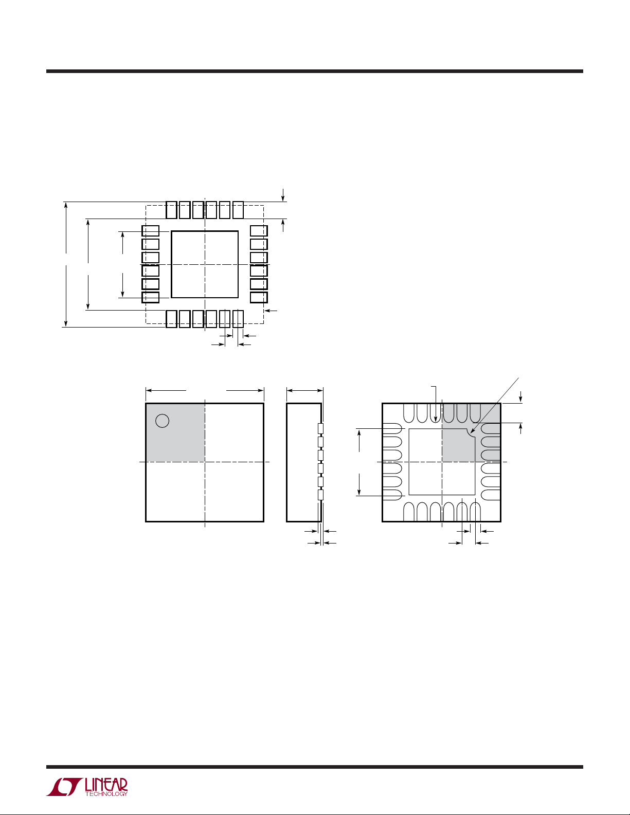
PACKAGE DESCRIPTION
LT3598
UF Package
24-Lead Plastic QFN (4mm × 4mm)
(Reference LTC DWG # 05-08-1697)
0.70 ±0.05
4.50 ± 0.05
3.10 ± 0.05
2.45 ± 0.05
(4 SIDES)
RECOMMENDED SOLDER PAD PITCH AND DIMENSIONS
4.00 ± 0.10
(4 SIDES)
PIN 1
TOP MARK
(NOTE 6)
NOTE:
1. DRAWING PROPOSED TO BE MADE A JEDEC PACKAGE OUTLINE MO-220 VARIATION (WGGD-X)—TO BE APPROVED
2. DRAWING NOT TO SCALE
3. ALL DIMENSIONS ARE IN MILLIMETERS
4. DIMENSIONS OF EXPOSED PAD ON BOTTOM OF PACKAGE DO NOT INCLUDE
MOLD FLASH. MOLD FLASH, IF PRESENT, SHALL NOT EXCEED 0.15mm ON ANY SIDE, IF PRESENT
5. EXPOSED PAD SHALL BE SOLDER PLATED
6. SHADED AREA IS ONLY A REFERENCE FOR PIN 1 LOCATION
ON THE TOP AND BOTTOM OF PACKAGE
0.25 ±0.05
0.50 BSC
PACKAGE OUTLINE
0.75 ± 0.05
2.45 ± 0.10
(4-SIDES)
0.200 REF
0.00 – 0.05
BOTTOM VIEW—EXPOSED PAD
R = 0.115
TYP
2423
PIN 1 NOTCH
R = 0.20 TYP OR
0.35 × 45° CHAMFER
0.40 ± 0.10
1
2
(UF24) QFN 0105
0.25 ± 0.05
0.50 BSC
Information furnished by Linear Technology Corporation is believed to be accurate and reliable.
However, no responsibility is assumed for its use. Linear Technology Corporation makes no representation that the interconnection of its circuits as described herein will not infringe on existing patent rights.
3598f
19
Page 20

LT3598
TYPICAL APPLICATION
90% Effi cient LED Driver for 60 White LEDs
PV
2.2μF
8V TO 40V
C1
60.4k
IN
V
IN
5V
C3
2.2μF
R1
51.1k
R8
R
10k
HOT
R
100k
NTC
SHDN
PWM
SYNC
R7
100k
100k
IN
OPENLED
SHDN
PWM
SYNC
RT
V
REF
CTRL
T
SETISET
C5
47pF
L1, 10μH
R3
14.7k
SWV
LT3598
SS GND
C4
10nF
D1
V
OUT
V
O_SW
R4
1.00M
FB
R5
30.9k
LED1
LED2
LED3
LED4
LED5
LED6
V
C
R
C
2.61k
C
C
15nF
RELATED PARTS
PART NUMBER DESCRIPTION COMMENTS
LT3474/
36V, 1A (I
LT3474-1
LT3475/
Dual 1.5A (I
LT3475-1
LT3476 Quad Output 1.5A, 2MHz High Current LED Driver with
1000:1 Dimming
LT3477 3A, 42V, 3MHz Boost, Buck-Boost, Buck LED Driver V
LT3478/LT3478-1 4.5A, 42V, 2.5MHz High Current LED Driver with 3000:1
Dimming
LT3486 Dual 1.3A, 2MHz High Current LED Driver V
LT3496 45V, 2.1MHz 3-Channel (I
LED Driver
LT3497 Dual 2.3MHz, Full Function LED Driver with Integrated
Schottkys and 250:1 True Color PWM Dimming
LT3498 2.3MHz, 20mA LED Driver and OLED Driver with
Integrated Schottky
LT3518/LT3517 2.3A/1.3A 45V, 2.5MHz Full Featured LED Driver with
True Color PWM Dimming
LT3590 48V, 850kHz 50mA Buck Mode LED Driver V
LT3592 36V, 2.2MHz, 500mA Buck Mode LED Driver
LT3595 45V, 2.5MHz 16-Channel Full Featured LED Driver V
), 2MHz, Step-Down LED Driver VIN: 4V to 36V, V
LED
), 36V, 2MHz, Step-Down LED Driver VIN: 4V to 36V, V
LED
I
< 1μA, TSSOP-16E Package
SD
I
< 1μA, TSSOP-20E Package
SD
: 2.8V to 16V, V
V
IN
I
< 10μA, 5mm × 7mm QFN-10 Package
SD
: 2.5V to 25V, V
IN
QFN and TSSOP20E Packages
VIN: 2.8V to 36V, V
I
< 3μA, TSSOP16E Package
SD
: 2.5V to 24V, V
IN
I
< 1μA, 5mm × 3mm DFN and TSSOP-16E Packages
SD
= 1A) Full Featured
LED
VIN: 3V to 30V (40V
3000:1, I
VIN: 2.5V to 10V, V
DFN-10 Package
V
: 2.5V to 12V, V
IN
DFN-10 Package
VIN: 3V to 30V (40V
3000:1, I
: 4.5V to 55V, Dimming = 200:1 True Color PWM, ISD < 15μA,
IN
2mm × 2mm DFN-6 and SC70 Packages
V
: 3.6V to 36V, True Color PWM Dimming = 10:1, ISD < 1μA, 2mm × 3mm
IN
DFN-10 and MSOP-10E Packages
: 4.5V to 55V, V
IN
ISD < 1μA, 5mm × 9mm QFN-56 Package
SD
SD
LED Current Matching vs Temperature
C2
4.7μF
20mA
3598 TA04a
= 13.5V, True Color PWM Dimming = 400:1,
OUT(MAX)
= 13.5V, True Color PWM Dimming = 3000:1,
OUT(MAX)
= 36V, True Color PWM Dimming = 1000:1,
OUT(MAX)
= 40V, Dimming = Analog/PWM, ISD < 1μA,
OUT(MAX)
= 42V, True Color PWM Dimming = 3000:1,
OUT(MAX)
= 36V, True Color PWM Dimming = 1000:1,
OUT(MAX)
), V
MAX
OUT(MAX)
< 1μA, 4mm × 3mm QFN-28 Package
= 32V, IQ = 6mA, ISD < 12μA, 2mm × 3mm
OUT(MAX)
= 32V, IQ = 1.65mA, ISD < 9μA, 2mm × 3mm
OUT(MAX)
), V
MAX
OUT(MAX)
< 5μA, 4mm × 4mm QFN-16 Package
= 45V, True Color PWM Dimming = 5000:1,
OUT(MAX)
100
95
90
85
80
75
EFFICIENCY (%)
70
65
60
20 40 8060 100
0
TOTAL LED CURRENT (mA)
= 45V, True Color PWM Dimming =
= 42V, True Color PWM Dimming =
VIN = 25V
VIN = 16V
120
3598 TA05b
20
Linear Technology Corporation
1630 McCarthy Blvd., Milpitas, CA 95035-7417
(408) 432-1900 ● FAX: (408) 434-0507
●
www.linear.com
3598f
LT 0908 • PRINTED IN USA
© LINEAR TECHNOLOGY CORPORATION 2008
 Loading...