

Linear Technology LT3595EUHH, LT3595 Datasheet
LT3595
1
3595f
, LT, LTC and LTM are registered trademarks of Linear Technology Corporation.
True Color PWM is a trademark of Linear Technology Corporation. All other trademarks are
the property of their respective owners.
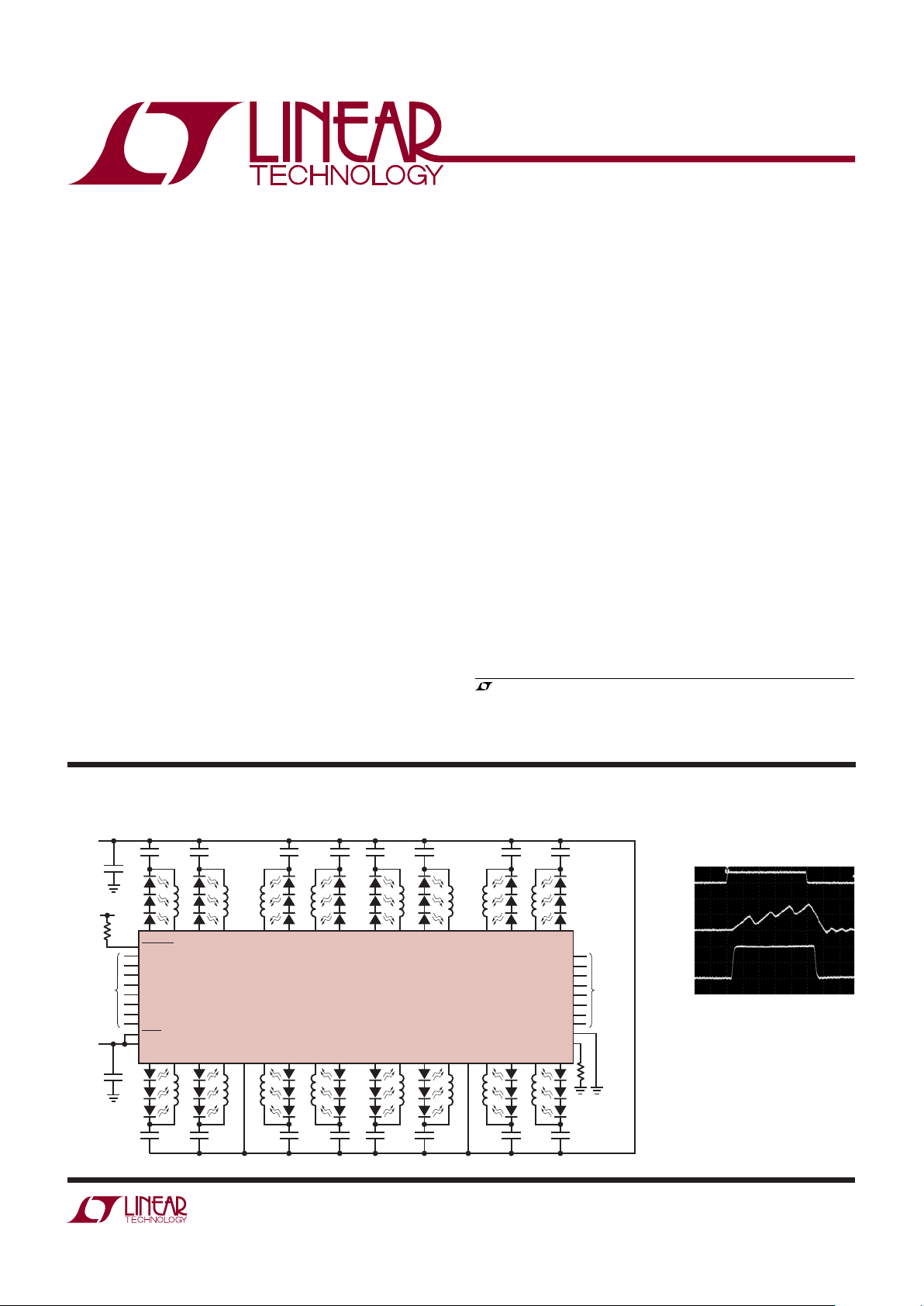
TYPICAL APPLICATION
FEATURES
APPLICATIONS
DESCRIPTION
16 Channel
Buck Mode LED Driver
The LT®3595 is a high performance LED Driver designed
to drive sixteen independent channels of up to 10 LEDs
at currents up to 50mA. Series connection of the LEDs
provides identical LED currents resulting in uniform brightness. Power switches, Schottky diodes, and compensation
components are all internal, providing a small converter
footprint and lower component cost. The high 2MHz
switching frequency permits the use of tiny, low profi le
inductors and capacitors. A fi xed frequency, current mode
architecture results in stable operation over a wide range
of supply and output voltage.
A single external resistor sets the LED current for all sixteen
channels, and dimming is then controlled for each channel
by pulse width modulating the individual PWM pins. Relative current matching among the sixteen drivers is 8% and
the PWM dimming range is 5000:1. The part is available
in a 5mm × 9mm × 0.75mm 56-pin QFN package.
16-Channel LED Driver (Three LEDs per Channel), 20mA Current
■
4.5V to 45V Input Supply Range
■
Up to 50mA LED Current per Channel
■
100mA, 45V Internal Switches
■
8% Relative LED Current Match at 20mA
■
16 Independent LED Channels
■
5000:1 True Color PWMTM Dimming Range
■
LEDs Disconnected in Shutdown
■
Internal Schottky Diodes
■
Low Quiescent Current
■
2MHz Switching Frequency
■
R
SET
Pin Sets Master LED Current
■
Typical Effi ciency: 92%
■
Open LED Detection and Thermal Protection
■
56-Pin 5mm × 9mm × 0.75mm QFN Package
■
LED Video Billboards
■
LCD Televisions
■
Stadium and Advertising Displays
5000:1 PWM
Dimming at 100Hz
V
IN
15V TO
45V
LED
BRIGHTNESS
CONTROL
V
CC
3V TO
5.5V
V
CC
0.47μF 0.47μF 0.47μF 0.47μF 0.47μF 0.47μF 0.47μF 0.47μF
0.47
μF
10
μF
10
μF
100k
75.0k
0.47μF 0.47μF 0.47μF 0.47μF 0.47μF 0.47μF 0.47μF
3595 TA01
OPENLED
PWM1
PWM2
PWM3
PWM4
PWM5
PWM6
PWM7
PWM8
V
CC
PWM9
PWM10
PWM11
PWM12
PWM13
PWM14
PWM15
PWM16
GND
R
SET
L1 SW1 SW2 L4SW3 SW7L3 SW4 L5 L6SW5 SW6L2 L7 SW8 L8
L16 SW16 SW15 V
IN
L13SW14 VINSW10L14 SW13 L12 L11SW12 SW11L15 L10 SW9 L9
100μH
100
μH
100
μH
100μH100
μH
100μH
100
μH
100μH
100
μH
100
μH
100
μH
100μH100
μH
100μH
100
μH
100μH
SHDN
LT3595
LED
BRIGHTNESS
CONTROL
400ns/DIV
I
LED
10mA/DIV
I
SW
20mA/DIV
V
PWM
5V/DIV
3595 TA01
b
V
IN
= 15V
3 LEDS AT 20mA
T = 10ms
T
ON
= 2μs
LT3595
2
3595f
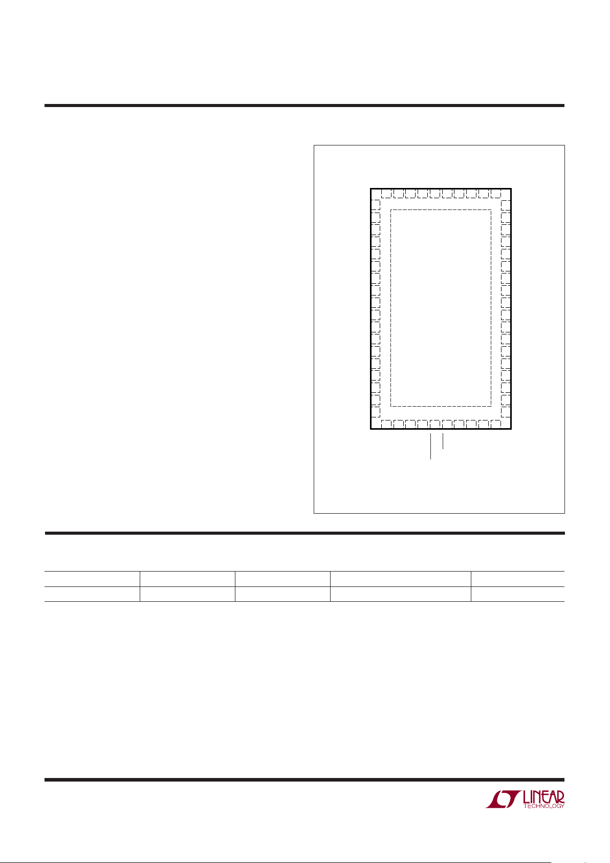
PIN CONFIGURATIONABSOLUTE MAXIMUM RATINGS
Input Voltage (VIN) ....................................................45V
L1-16 Voltage ...........................................................45V
Supply Voltage (V
CC
) ..................................................6V
R
SET
, ⎯O⎯P⎯E⎯N⎯L⎯E⎯D , PWM1-16, ⎯S⎯H⎯D⎯N Voltage ...............6V
Operating Junction Temperature Range
(Note 2) ...............................................–40°C to 85°C
Maximum Junction Temperature .......................... 125°C
Storage Temperature Range ...................–65°C to 125°C
(Note 1)
19 20 21 22
TOP VIEW
57
UHH PACKAGE
56-LEAD (5mm × 9mm) PLASTIC QFN
23 24 25 26 27 28
56 55 54 53 52 51 50 49 48 47
39
40
41
42
43
44
45
46
8
7
6
5
4
3
2
1L16
SW16
L15
SW15
V
IN
SW14
L14
SW13
L13
L12
SW12
L11
SW11
V
IN
SW10
L10
SW9
L9
L1
SW1
L2
SW2
NC
SW3
L3
SW4
L4
L5
SW5
L6
SW6
NC
SW7
L7
SW8
L8
PWM16
PWM15
PWM14
PWM13
VCCR
SET
PWM4
PWM3
PWM2
PWM1
38
37
36
35
34
33
32
31
30
29
9
10
11
12
13
14
15
16
17
18
PWM9
PWM10
PWM11
PWM12
OPENLED
SHDN
PWM5
PWM6
PWM7
PWM8
T
JMAX
= 125°C, θJA = 31°C/W, θJC = 0.5°C/W
EXPOSED PAD (PIN 57) IS GND, MUST BE SOLDERED TO PCB
ORDER INFORMATION
LEAD FREE FINISH TAPE AND REEL PART MARKING PACKAGE DESCRIPTION TEMPERATURE RANGE
LT3595EUHH#PBF LT3595EUHH#TRPBF 3595 56-Lead (5mm × 9mm) Plastic QFN –40°C to 85°C
Consult LTC Marketing for parts specifi ed with wider operating temperature ranges.
Consult LTC Marketing for information on non-standard lead based fi nish parts.
For more information on lead free part marking, go to: http://www.linear.com/leadfree/
For more information on tape and reel specifi cations, go to: http://www.linear.com/tapeandreel/
LT3595
3
3595f
ELECTRICAL CHARACTERISTICS
Note 1: Stresses beyond those listed under Absolute Maximum Ratings
may cause permanent damage to the device. Exposure to any Absolute
Maximum Rating condition for extended periods may affect device
reliability and lifetime.
PARAMETER CONDITIONS MIN TYP MAX UNITS
V
IN
Operating Voltage
4.5 V
V
CC
Operating Voltage
3 5.5 V
V
CC
Input Under Voltage Lockout
2.6 2.9 V
I
VIN
Quiescent Current ON, No Switching VIN = 45V 0.25 mA
I
VIN
Quiescent Current in Shutdown VIN = 45V, ⎯S⎯H⎯D⎯N = 0V 15 40 μA
I
VCC
Quiescent Current ON, No Switching VCC = 3.3V 17 mA
I
VCC
Quiescent Current in Shutdown VCC = 3.3V, ⎯S⎯H⎯D⎯N = 0V 3 10 μA
I
L1-16
Output Current Accuracy R
SET
= 75.0kΩ 18.4 20 21.6 mA
Switching Frequency 1.622.4MHz
Maximum Duty Cycle
●
78 83 %
Switch Current Limit
●
90 120 150 mA
Switch V
CESAT
ISW1-16 = 50mA 450 mV
Switch Leakage Current VSW1-16 = 45V 0.1 6 μA
Schottky Forward Drop I
SCHOTTKY
= 50mA 0.8 V
Schottky Leakage Current V
IN
= 45V, V
SW1-16
= 0.7V, ⎯S⎯H⎯D⎯N = 0V 0.1 4 μA
⎯S⎯H⎯D⎯
N, PWM1-16 Input Low Voltage 0.4 V
⎯S⎯H⎯D⎯
N, PWM1-16 Input High Voltage 1.6 V
⎯S⎯H⎯D⎯
N Pin Bias Current
⎯S⎯H⎯D⎯
N = 3.3V 35 μA
PWM1-16 Pin Bias Current PWM1-16 = 3.3V 0.1 1 μA
⎯O⎯P⎯E⎯N⎯L⎯E⎯
D Pin Voltage VCC = 3.3V, I
⎯O⎯P⎯E⎯N⎯L⎯E⎯
D
= 200μA 0.12 V
⎯O⎯P⎯E⎯N⎯L⎯E⎯
D Pin Input Leakage Current
⎯O⎯P⎯E⎯N⎯L⎯E⎯
D = 3.3V 0.1 1 μA
The ● denotes the specifi cations which apply over the full operating
temperature range, otherwise specifi cations are at T
A
= 25°C, VIN = 45V, VCC = 3.3V, PWM = ⎯S⎯H⎯D⎯N = ⎯O⎯P⎯E⎯N⎯L⎯E⎯D = 3.3V, R
SET
= 75kΩ,
GND = 0V, unless otherwise noted.
Note 2: The LT3595 is guaranteed to meet performance specifi cations
from 0°C to 85°C junction temperature. Specifi cations over the – 40°C
to 85°C operating junction temperature range are assured by design,
characterization and correlation with statistical process controls.
LT3595
4
3595f
R
SET
RESISTANCE (kΩ)
25
LED CURRENT (mA)
30
50
40
60
50 150
20
10
0
75 100 125
3595 G05
DUTY CYCLE (%)
0.01
LED CURRENT (mA)
1
10
100
0.1
0.01
0.001
0.1
1
10
100
3595 G04
VIN = 45V
10 LEDS AT 20mA
PWM FREQUENCY = 100Hz
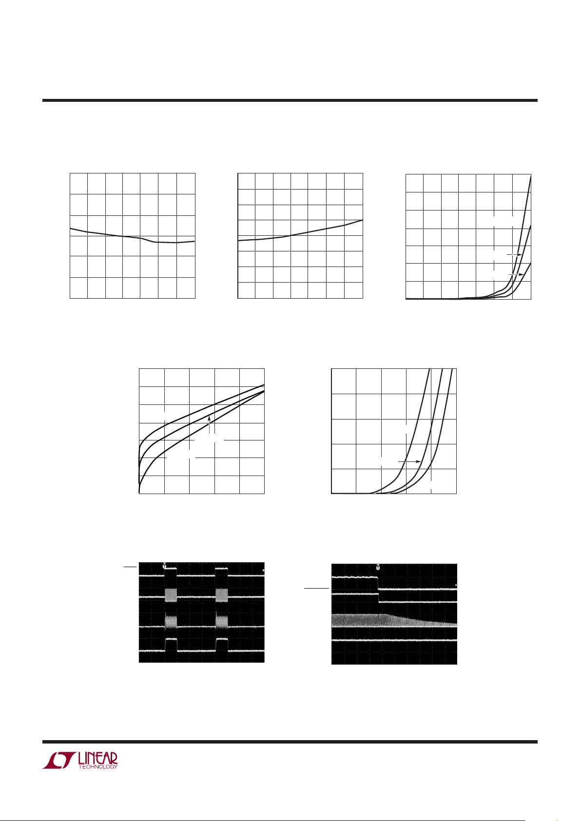
TYPICAL PERFORMANCE CHARACTERISTICS
Switching Waveforms
PWM Dimming Waveforms
(1000:1)
LED Current vs PWM Duty Cycle
Wide Dimming Range (5000:1)
LED Current vs R
SET
Resistance
VIN Quiescent Current
VCC Quiescent Current
⎯S⎯H⎯D⎯
N Pin Bias Current
PWM Dimming Waveforms
(10:1)
VIN (V)
0
V
IN
CURRENT (mA)
1.2
1.6
2.0
40
0.8
0.4
0
10
20
30
50
3595 G06
T = 25°C
T = 125°C
T = – 40°C
400ns/DIV
10 LEDS
V
SW1
50V/DIV
10 LEDS
I
L1
50mA/DIV
5 LEDS
V
SW2
50V/DIV
5 LEDS
I
L2
50mA/DIV
3595 G01
V
IN
= 45V
I
LED
= 20mA
2μs/DIV
I
LED
20mA/DIV
I
L
20mA/DIV
PWM
5V/DIV
3595 G02
V
IN
= 40V
10 LEDS AT 20mA
PWM FREQUENCY = 100H
z
TON = 10μs
2ms/DIV
I
LED
20mA/DIV
I
L
20mA/DIV
PWM
5V/DIV
3595 G03
V
IN
= 40V
10 LEDS AT 20mA
PWM FREQUENCY = 100H
z
TON = 1ms
V
CC
(V)
0
0
V
CC
CURRENT (mA)
2
6
8
10
20
14
2
4
5
4
16
18
12
1
3
6
7
3595 F07
T = 125°C
T = –40°C
T = 25°C
VCC = 3.3V
0
0
20
40
60
80
100
1
234
56
3595 F08
T = 125°C
T = –40°C
I
SHDN
(μA)
T = 25°C
V
SHDN
(V)
LT3595
5
3595f
Current Limit vs Temperature
TYPICAL PERFORMANCE CHARACTERISTICS
Switching Frequency
vs Temperature
Schottky Leakage Current
vs Temperature
Switch Saturation Voltage
(V
CESAT
)
Schottky Forward Voltage Drop
Transient Response
⎯O⎯P⎯E⎯N⎯L⎯E⎯
D Waveforms
TEMPERATURE (°C)
–50
130
140
150
25 75
120
110
–25 0
50 100 125
100
90
CURRENT LIMIT (mA)
3595 G09
TEMPERATURE (°C)
–50
2.0
2.2
2.1
2.3
2.4
25 75
1.9
1.8
–25 0
50 100 125
1.7
1.6
SWITCHING FREQUENCY (MHz)
3595 G10
TEMPERATURE (°C)
–50
0.8
1.0
1.4
25 75
0.6
0.4
–25 0
50 100 125
0.2
0
1.2
SCHOTTKY LEAKAGE CURRENT (μA)
3595 G11
VIN = 45V
VIN = 24V
VIN = 4.5V
SWITCH CURRENT (mA)
0
500
600
700
80
400
300
20 40 60 100
200
100
0
SWITCH SATURATION VOLTAGE (mV)
T = 125°C
T = –40°C
T = 25°C
SCHOTTKY FORWARD DROP (V)
0
SCHOTTKY FORWARD CURRENT (mA)
60
80
100
0.8
40
20
0
0.2
0.4
0.6
1
3595 G13
T = 125°C
T = – 40°C
T = 25°C
100μs/DIV
V
SW
50V/DIV
I
SW
50mA/DIV
I
LED
20mA/DIV
3595 G1
4
V
IN
= 45V
10 LEDS AT 20mA
V
SHDN
5V/DIV
20μs/DIV
V
SW
CH 1
50V/DIV
I
LED
CH 2
20mA/DIV
I
LED
CH 1
20mA/DIV
3595 G1
5
OPENLED
5V/DIV
V
IN
= 45V
10 LEDS AT 20mA
 Loading...