

Page 1
LT3593
1MHz White LED Driver with
Output Disconnect and One
Pin Current Programming
FEATURES
n
Drives Up to Ten White LEDs from a 3V Supply
n
One Pin Shutdown and Current Programming
n
LEDs Disconnected in Shutdown
n
32:1 Linear Brightness Control Range
n
VIN Range: 2.7V to 5.5V
n
±5% Output Current Accuracy at Full Scale
n
Low Shutdown Current: 3µA
n
1MHz Switching Frequency
n
Requires Only 1µF Output Capacitor
n
Low Profi le 6-Lead DFN (2mm × 2mm × 0.75mm)
and 6-Lead SOT-23 Packages
APPLICATIONS
n
Cell Phones
n
Digital Cameras
n
PDAs, Handheld Computers
n
MP3 Players
n
GPS Receivers
DESCRIPTION
The LT®3593 is a step-up DC/DC converter designed to
drive up to ten white LEDs in series from a Li-Ion cell.
Series connection of the LEDs provides identical LED
currents and eliminates the need for ballast resistors. The
device features a unique high side LED current sense that
enables the part to function as a “one wire current source”
where the low side of the LED string can be returned to
ground anywhere.
Additional features include output disconnect in shutdown,
open LED protection and 1-pin shutdown/LED current
control. The CTRL pin is toggled to adjust the LED current
via an internal counter and a 5-bit DAC.
The LT3593 switches at 1MHz, allowing the use of tiny
external components. Constant frequency switching results in low input noise and a small output capacitor. The
LT3593 is available in the 6-lead DFN (2mm × 2mm) as
well as the 6-lead SOT-23 packages.
L, LT, LTC and LTM are registered trademarks of Linear Technology Corporation.
All other trademarks are the property of their respective owners.
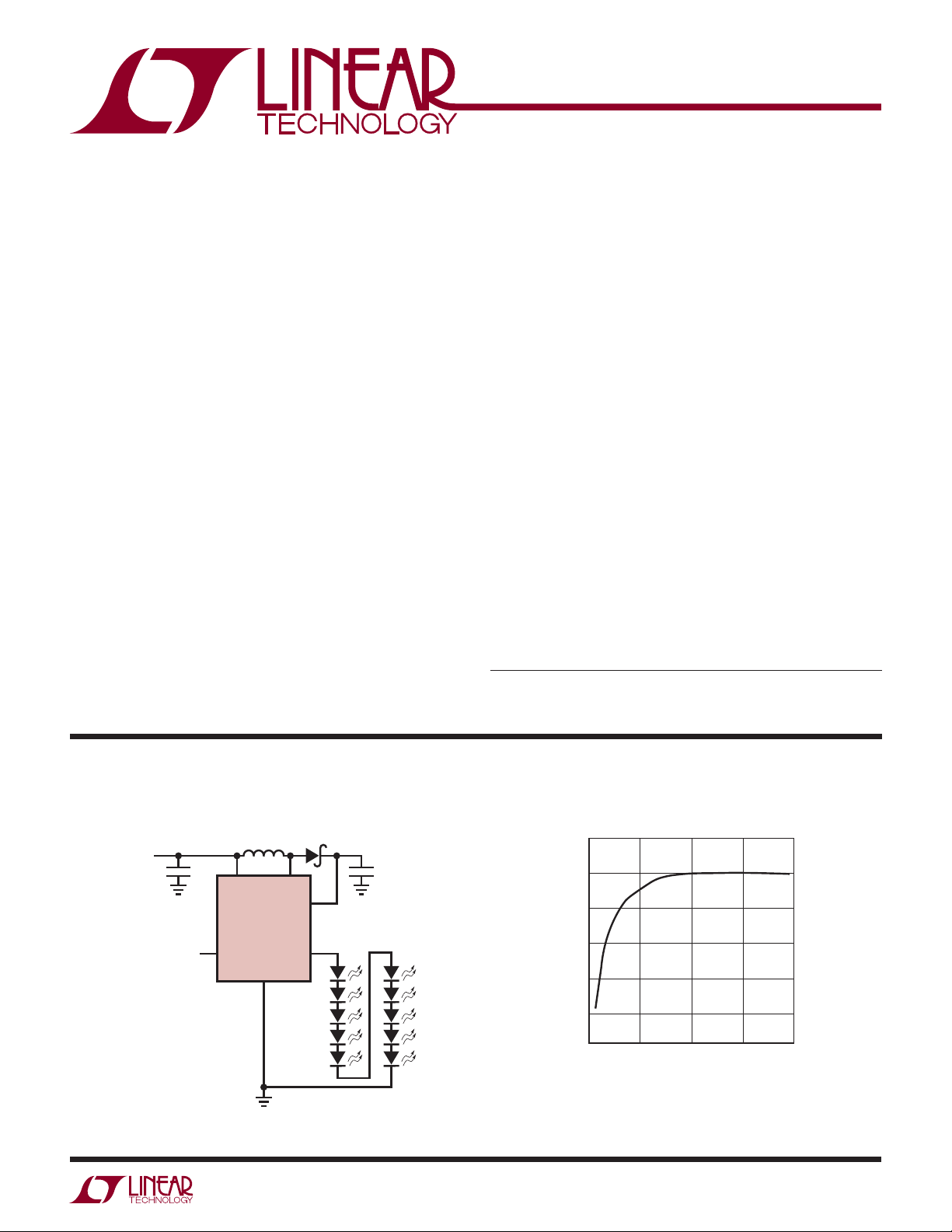
TYPICAL APPLICATION
Li-Ion Driver for Ten White LEDs
V
CTRL
IN
10µH
SW
CAP
LT3593
LED
GND
V
IN
3V TO 5V
SHUTDOWN AND
CURRENT CONTROL
1µF 1µF
3593 TA01a
Conversion Effi ciency
90
VIN = 3.6V
10 LEDs
80
70
60
EFFI CIENCY (%)
50
40
30
0
10
LED CURRENT (mA)
20155
3593 TA01b
3593f
1
Page 2
LT3593
ABSOLUTE MAXIMUM RATINGS
Input Voltage ...............................................................6V
CTRL Voltage ..............................................................6V
SW Voltage ...............................................................45V
CAP Voltage ..............................................................45V
LED Voltage ..............................................................45V
PIN CONFIGURATION
TOP VIEW
6
1
V
IN
GND
CTRL
6-LEAD (2mm × 2mm) PLASTIC DFN
T
EXPOSED PAD (PIN 7) IS GND, MUST BE SOLDERED TO PCB
7
2
3
DC PACKAGE
= 125°C, θJA = 106°C/W
JMAX
SW
5
CAP
LED
4
(Note 1)
Operating Junction Temperature Range
(Note 2) .................................................... –40°C to 85°C
Maximum Junction Temperature........................... 125°C
Storage Temperature Range ................... –65°C to 150°C
Lead Temperature (Soldering, 10 sec)
TSOT Package ................................................... 300°C
TOP VIEW
CTRL 1
GND 2
V
3
IN
S6 PACKAGE
6-LEAD PLASTIC TSOT-23
T
= 125°C, θJA = 192°C/W
JMAX
6 LED
5 CAP
4 SW
ORDER INFORMATION
LEAD FREE FINISH TAPE AND REEL PART MARKING PACKAGE DESCRIPTION TEMPERATURE RANGE
LT3593EDC#PBF LT3593EDC#TRPBF LDBR
LT3593ES6#PBF LT3593ES6#TRPBF LTDBS 6-Lead Plastic TSOT-23 –40°C to 85°C
Consult LTC Marketing for parts specifi ed with wider operating temperature ranges.
Consult LTC Marketing for information on non-standard lead based fi nish parts.
For more information on lead free part marking, go to: http://www.linear.com/leadfree/
For more information on tape and reel specifi cations, go to: http://www.linear.com/tapeandreel/
ELECTRICAL CHARACTERISTICS
The l denotes the specifi cations which apply over the full operating
temperature range, otherwise specifi cations are at TA = 25°C. VIN = 3.6V, V
PARAMETER CONDITIONS MIN TYP MAX UNITS
Operating Voltage Range 2.7 5.5 V
Supply Current Not Switching; During Current Programming 300 µA
CTRL = 0 3 10 µA
Switching Frequency 0.85 1 1.15 MHz
Maximum Duty Cycle 92 94 %
Switch Current Limit 550 700 mA
Switch V
CESAT
ISW = 250mA 250 mV
6-Lead (2mm × 2mm) Plastic DFN
= 3.6V, unless otherwise specifi ed.
CTRL
–40°C to 85°C
2
3593f
Page 3
LT3593
ELECTRICAL CHARACTERISTICS
The l denotes the specifi cations which apply over the full operating
temperature range, otherwise specifi cations are at T
PARAMETER CONDITIONS MIN TYP MAX UNITS
Switch Leakage Current V
– V
LED Pin Voltage Drop (V
LED Pin Leakage Current CTRL = 0, V
CTRL High Threshold 1.6 V
CTRL Low Threshold 0.4 V
CTRL t
PW
CTRL t
SD
CTRL t
EN
Full-Scale LED Current V
LED Current Programming Resolution Linear Increments 625 µA
LED Current Limit 45 mA
CTRL Pin Bias Current V
Overvoltage Protection
CAP
)I
LED
= 25°C. VIN = 3.6V, V
A
= 30V 1 µA
SW
= 20mA 250 mV
LED
= 35V 1 µA
CAP
Programming Pulse Width (Note 3) 250 ns
Time from CTRL = 0 to Shutdown 95 128 200 µs
Time from CTRL = 1 to Enable 95 128 200 µs
= 16V
CAP
V
= 16V
CAP
= 5.5V 1 µA
CTRL
= 3.6V, unless otherwise specifi ed.
CTRL
19
l
18.5
l
36 38 40 V
20
20
21
21.5
mA
mA
Note 1: Stresses beyond those listed under Absolute Maximum Ratings
may cause permanent damage to the device. Exposure to any Absolute
Maximum Rating condition for extended periods may affect device
reliability and lifetime.
Note 2: The LTC3593E is guaranteed to meet performance specifi cations
from 0°C to 85°C operating junction temperature range. Specifi cations
over the –40°C to 85°C operating junction temperature range are assured
by design, characterization and correlation with statistical process
controls.
Note 3: Guaranteed by design.
3593f
3
Page 4
LT3593
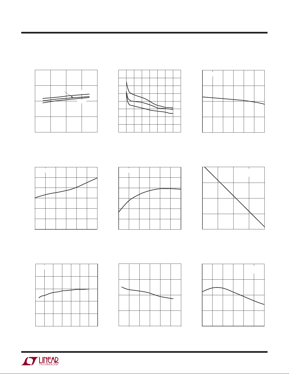
TYPICAL PERFORMANCE CHARACTERISTICS
Switch Saturation Voltage
)
(V
CESAT
600
500
400
300
200
100
SWITCH SATURATION VOLTAGE (mV)
0
0
100 500
SWITCH CURRENT (mA)
LED Pin Voltage Drop
– V
(V
CAP
LED
300
VIN = 3.6V
= 16V
V
CAP
250
200
(mV)
LED
150
– V
CAP
100
V
50
100°C
25°C
–50°C
400200
600300
3593 G01
)
100°C
25°C
–50°C
Shutdown Current (V
6
5
4
3
2
SHUTDOWN CURRENT (µA)
1
0
2
VIN (V)
LED Pin Current Limit
46
45
44
43
LED PIN CURRENT LIMIT (mA)
CTRL
100°C
25°C
= 0V)
53
VIN = 3.6V
V
CAP
= 25°C unless otherwise specifi ed.
T
A
Quiescent Current (V
3.50
3.25
3.00
–50°C
64
3593 G02
2.75
2.50
QUIESCENT CURRENT (mA)
2.25
2.00
2
Switching Current Limit vs
Temperature
750
VIN = 3.6V
= 16V
700
650
600
SWITCH CURRNET LIMIT (mA)
VIN (V)
CTRL
100°C
25°C
–50°C
= 3.6V)
53
3593 G03
64
4
0
0
LED CURRENT (mA)
155
2010
3593 G04
Switching Waveform
I
L
200mA/DIV
V
CAP
200mV/DIV
AC COUPLED
V
SW
20V/DIV
FRONT PAGE
APPLICATION CIRCUIT
1µs/DIVVIN = 3.6V
42
–50
TEMPERATURE (°C)
750–25 25
10050
3593 G05
550
–50
25 50 75–25
TEMPERATURE (°C)
1000
3593 G06
Transient Response
V
CTRL
5V/DIV
I
L
200mA/DIV
V
CAP
10V/DIV
3393 G08
3593f
3393 G07
= 3.6V
IN
FRONT PAGE
APPLICATION CIRCUIT
200µs/DIVV
Page 5
LT3593
TYPICAL PERFORMANCE CHARACTERISTICS
Open-Circuit Output Clamp
Voltage
40
39
25°C
38
37
OPEN-CIRCUIT CLAMP VOLTAGE (V)
36
2
VIN (V)
Input Current in Output
Open-Circuit vs Temperatue
8
VIN = 3.6V
7
6
100°C
–50°C
543
6
3593 G09
Input Current in Output Open
Circuit
10
9
8
7
6
5
4
3
INPUT CURRENT OUTPUT OPEN-CIRCUIT (mA)
2
2.0 2.5
VIN (V)
5.0 5.53.0 3.5
Switching Frequency vs
Temperature
1150
VIN = 3.6V
1100
1050
TA = 25°C unless otherwise specifi ed.
Open-Circuit Output Clamp
Voltage vs Temperature
40
VIN = 3.6V
39
38
37
OPEN-CIRCUIT CLAMP VOLTAGE (V)
6.04.0 4.5
3593 G10
36
–50
TEMPERATURE (°C)
LED Current vs CTRL Strobe
Pulses
20
15
750–25 25
VIN = 3.6V
10LEDS
10050
3593 G11
5
4
3
INPUT CURRENT OUTPUT OPEN-CIRCUIT (mA)
2
–50
Full-Scale Current vs V
21.0
10 LEDs
20.5
20.0
LED CURRENT (mA)
19.5
19.0
2.5
TEMPERATURE (°C)
IN
5.03.53.0 4.0
VIN (V)
1000
950
SWITCHING FREQUENCY (kHz)
900
750–25 25
10050
3593 G12
850
–50
TEMPERATURE (°C)
10050
750–25 25
3593 G13
10
LED CURRENT (mA)
5
0
0
NUMBER OF CTRL STROBES
16824
32
3593 G14
Full-Scale Current vs
Temperature
21.0
20.5
20.0
19.5
FULL SCALE CURRENT (mA)
19.0
–50
0–25 50 7525
TEMPERATURE (°C)
VIN = 3.6V
10LEDS
100
3593 G17
6.05.54.5
3593 G15
Full-Scale Current vs V
21.0
20.5
20.0
LED CURRENT (mA)
19.5
19.0
5
CAP
35
3593 G16
CAP
25201510 30
(V)
V
3593f
5
Page 6

LT3593
PIN FUNCTIONS
(DFN/TSOT)
VIN (Pin 1/Pin 3): Input Supply Pin. Must be locally by-
passed with a 1F X5R or X7R type ceramic capacitor.
GND (Pin 2/Pin 2): Ground Pin. Connect directly to local
ground plane.
SW (Pin 6/Pin 4): Switch Pin. Connect inductor between
this pin and the V
pin. Minimize inductance at this pin
IN
to minimize EMI.
CAP (Pin 5/Pin 5): Output Pin. Connect to output capacitor. Minimize trace between this pin and output capacitor
to reduce EMI.
CTRL (Pin 3/Pin 1): Current Control and Shutdown Pin.
This pin is used to program the LED output current. This
pin is strobed up to 32 times to decrement the internal
5-bit DACs from full-scale to 1LSB. The counter will stop
at 1LSB if the strobing continues beyond 32 counts.
The pin must be held high after the fi nal desired positive
strobe edge. The data is transferred after a 128s (typ)
delay. The part can be reprogrammed to a different value
after it has been enabled, however the current will change
to the new value after 128µs. If CTRL is held low for longer
than 128s (typ), the part will go into shutdown.
LED (Pin 4/Pin 6): LED Pin. An internal switch connects
this pin to CAP. The top of the LED string is connected
to this pin. When the part is in shutdown, the LED pin is
switched off from CAP so no current runs through the
LEDs. The switch is also used to sense the LED current
when the part is on.
Exposed Pad (Pin 7/NA): Ground. The Exposed Pad must
be soldered to the PCB.
BLOCK DIAGRAM
SHDN
PIN NUMBERS REFER TO DFN PACKAGE. REFER TO PIN CONFIGURATION FOR TSOT PIN NUMBERS
V
1.24V
REF
61
IN
PWM
–
COMP
A2
+
R
S
DRIVER
Q
SWV
Q1
OVERVOLTAGE
PROTECTION
CAP
5
+
+
–
RAMP
GENERATOR
OSCILLATOR
A3
–
A1
R
C
C
C
+
–
R
M2 M1
5-BIT
LINEAR DAC
5-BIT
COUNTER
GND
27 3
CTRL
SHDN
SHDN
LED
4
3593 F01
6
Figure 1. Block Diagram
3593f
Page 7

OPERATION
LT3593
The LT3593 uses a constant frequency, current mode
control boost scheme to provide excellent line and load
regulation. Operation can be best understood by referring
to the Block Diagram in Figure 1.
Output Disconnect
An internal switch connects between the CAP pin and the
LED pin. The top of the LED string is connected to the
LED pin. The string can be terminated to ground or to
if a low number of LEDs are driven. When the part is
V
IN
in shutdown, the switch is off; allowing no current to run
through the LEDs.
Current Programming
The LED current can be set to 32 different values
(625µA – 20mA) by strobing the CTRL pin. A 5-bit
counter is decremented by 1 on a CTRL pin rising edge,
reducing the programmed current by 625µA each time.
The desired current can be calculated by:
I
= 20mA – (N – 1) • 625µA
LED
where N is the number of rising edges. When the desired
current setting is reached, the CTRL pin must stay high.
128µs after the last rising edge on the CTRL pin, the
regulator will enable the output and start to regulate the
LED current to the programmed value. Figure 2 shows
an example of how the part can be programmed.
If a different current is desired, the CTRL pin can be strobed
again. The fi rst falling edge will reset the internal register
to the 20mA setting. While the new current is being programmed, the device will continue to regulate the previously
programmed value until the CTRL pin has remained high
for at least 128µs, at which time the regulated current will
slew to the newly programmed value. Figure 3 shows how
to program a new LED current level.
If the CTRL pin is held low for longer than 128µs, the part
will go into the shutdown mode.
CTRL
CTRL 17.5mA
CTRL 15mA
CTRL 12.5mA
Figure 2. Current Programming
128µs
CTRL
20mA 20mA
LED
CURRENT
Figure 3. Current Programming and Shutdown Timing
128µs 128µs
17.5mA 17.5mA
FULL CURRENT
20mA
3593 F02
SHDN
3593 F03
3593f
7
Page 8

LT3593
APPLICATIONS INFORMATION
Inductor Selection
A 10µH inductor is recommended for most LT3593 applications. Although small size and high effi ciency are
major concerns, the inductor should have low core losses
at 1MHz and low DCR (copper wire resistance). Some
inductors in this category with small size are listed in
Table 1. The effi ciency comparison of different inductors
is shown in Figure 4.
Table 1. Recommended Inductors
()
CURRENT
RATING
(mA) VENDOR
650
450
500
490
580
400
Murata
TDK
TOKO
L
PART
LQH43CN100
LQH32CN100
NR3010T100M 10 0.45 500 Taiyo Yuden
VLF4012AT-100M
VLF3010AT-100M
DE2812-1098AS-100M
DB3015C-1068AS-100M1010
90.00
80.00
70.00
DCR
(μH)
10100.24
0.44
10100.20
0.58
0.29
0.38
Table 2 shows a list of several ceramic capacitor manufacturers. Consult the manufacturers for detailed information
on their entire selection of ceramic parts.
Table 2. Recommended Ceramic Capacitor Manufacturers
Taiyo Yuden (408) 573-4150
AVX (803) 448-9411
Murata (714) 852-2001
Kemet (408) 986-0424
www.t-yuden.com
www.avxcorp.com
www.murata.com
www.kemet.com
Diode Selection
Schottky diodes, with their low forward voltage drop and
fast reverse recovery, are the ideal choices for LT3593 applications. The forward voltage drop of a Schottky diode
represents the conduction losses in the diode, while the
diode capacitance (C
or CD) represents the switching
T
losses. For diode selection, both forward voltage drop and
diode capacitance need to be considered. Schottky diodes
with higher current ratings usually have lower forward
voltage drop and larger diode capacitance, which can
cause signifi cant switching losses at the 1.0MHz switching
frequency of the LT3593. A Schottky diode rated at 400mA
to 500mA is suffi cient for most LT3593 applications. Some
recommended Schottky diodes are listed in Table 3.
60.00
NR3010T100M
EFFI CIENCY (%)
50.00
40.00
30.00
0.00
VLF4012-AT-100MR50
LQH43CN100K03
VLF3010AT-100MR49
LQH32CN100K53
DB3015C-1068AS-100M
10.00
LED CURRENT (mA)
20.0015.005.00
3593 F04
Figure 4. Effi ciency Comparison of Different Inductors
Capacitor Selection
The small size of ceramic capacitors makes them ideal
for LT3593 applications. Use only X5R and X7R types
because they retain their capacitance over wider voltage
and temperature ranges than other types such as Y5V or
Z5U. A 1µF input capacitor and a 1µF output capacitor are
suffi cient for most applications.
8
Table 3. Recommended Schottky Diodes
PART
NUMBER
CMDSH05-4 500 0.47 at
CMMSH1-40 1000 0.55 at 1A80 at 4V
ZLL5400 520 0.50 at
PMEG4005AEA
FORWARD
CURRENT
(mA)
VOLTAGE
DROP
(V)
500mA
400mA
500 0.47 at
500mA
DIODE
CAPACITANCE
(pF) MANUFACTURER
50 at 1V Central
15 at 30V Zetex
50 at 1V Phillips
631-435-1110
www.centralsemi.com
631-543-7100
www.zetex.com
+3140 27 24825
www.semiconductors.
phillips.com
3593f
Page 9

APPLICATIONS INFORMATION
LT3593
Overvoltage Protection
The LT3593 has an internal open-circuit protection circuit.
In the case of an output open circuit, when the LEDs are
disconnected from the circuit or the LEDs fail open, V
CAP
is clamped at 38V. The LT3593 will then switch at a very
low frequency to minimize input current. V
and input
CAP
current during output open circuit are shown in the Typical
Performance Characteristics. Figure 5 shows the transient
response when the LEDs are disconnected.
I
L
200mA/DIV
V
CAP
20V/DIV
Low Input Voltage Applications
The LT3593 can be used in low input voltage applications.
The input supply voltage to the LT3593 must be 2.7V or
higher, but the inductor can be run off a lower battery
voltage. This technique allows the LEDs to be powered off
two alkaline cells. Most portable devices have a 3.3V logic
supply voltage which can be used to power the LT3593.
The LEDs can be driven straight from the battery, resulting
in higher effi ciency.
Figure 6 shows three LEDs powered by two AA cells.
The battery is connected to the inductors and the chip is
powered off a 3.3V logic supply voltage.
L1
µH
2 AA CELLS
2V TO 3.2V
3.3V
SHUTDOWN AND
CURRENT CONTROL
10
C1
µF
1
V
IN
C3
µF
1
CTRL
SW
LT3593
GND
CAP
LED
D1
C2
µF
1
V
SW
20V/DIV
FRONT PAGE
APPLICATION CIRCUIT
400µs/DIVVIN = 3.6V
LEDs DISCONNECTED
AT THIS INSTANT
Figure 5. Output Open-Circuit Waveform
3593 F05
3593 F06
C1: TAIYO YUDEN EMK107B5105MA
C2: MURATA GRM31MR71H105KA88
L1: MURATA LQH43CN100
D1: CENTRAL CMDSH05-4
Figure 6. Two AA Cells to Three White LEDs
3593f
9
Page 10

LT3593
APPLICATIONS INFORMATION
Board Layout Considerations
As with all switching regulators, careful attention must
be paid to the PCB layout and component placement. To
prevent electromagnetic interference (EMI) problems,
proper layout of high frequency switching paths is essential.
Minimize the length and area of all traces connected to the
L1 L1
V
IN
CTRL
GND
C1
1
2
3
DFN Package TSOT-23 Package
6
5
7
4
C2
D1
Switching node pin (SW). Keep the sense voltage pins (CAP
and LED) away from the switching node. Place C2 next to
the CAP pin. Always use a ground plane under the switching
regulator to minimize interplane coupling. Recommended
component placement is shown in Figure 7.
V
IN
D1
43
52
61
C2
C1
CTRL
GND
3593 F07
Figure 7. Recommended Component Placement
10
3593f
Page 11

TYPICAL APPLICATIONS
LT3593
Li-Ion Driver for One White LED
V
IN
CTRL
10
LT3593
GND
V
IN
3V TO 5V
SHUTDOWN AND
CURRENT CONTROL
C1: TAIYO YUDEN EMK107BJ105MA
C2: TAIYO YUDEN GMK316BJ105ML
L1: MURATA LQH43CN100
D1: CENTRAL CMDSH05-4
C1
µF
1
Li-Ion Driver for Two White LED
V
CTRL
10
IN
LT3593
V
IN
3V TO 5V
SHUTDOWN AND
CURRENT CONTROL
C1: TAIYO YUDEN EMK107BJ105MA
C2: TAIYO YUDEN GMK316BJ105ML
L1: MURATA LQH43CN100
D1: CENTRAL CMDSH05-4
C1
µF
1
L1
µH
L1
GND
Conversion Effi ciency
70
VIN = 3.6V
1 LED
60
50
40
EFFICIENCY (%)
30
20
10
0
10
LED CURRENT (mA)
20155
3593 TA02b
SW
C2
1
CAP
LED
µF
D1
3593 TA02a
Conversion Effi ciency
80
VIN = 3.6V
C2
µF
1
µH
D1
SW
CAP
LED
3593 TA03a
2 LEDs
70
60
50
EFFICIENCY (%)
40
30
20
0
10
LED CURRENT (mA)
20155
3593 TA03b
3593f
11
Page 12

LT3593
TYPICAL APPLICATIONS
Li-Ion Driver for Three White LEDs
L1
10
µH
V
IN
3V TO 5V
SHUTDOWN AND
CURRENT CONTROL
C1
µF
1
V
IN
LT3593
CTRL
GND
C1: TAIYO YUDEN EMK107BJ105MA
C2: TAIYO YUDEN GMK316BJ105ML
L1: MURATA LQH43CN100
D1: CENTRAL CMDSH05-4
D1
SW
CAP
LED
3593 TA04a
Li-Ion Driver for Four White LEDs
L1
D1
µH
V
IN
3V TO 5V
SHUTDOWN AND
CURRENT CONTROL
C1
1
10
µF
V
SW
IN
CAP
LT3593
CTRL
LED
GND
Effi ciency
90
VIN = 3.6V
C2
µF
1
3 LEDs
80
70
60
EFFICIENCY (%)
50
40
30
0
10
LED CURRENT (mA)
20155
3593 TA04b
Effi ciency
90
VIN = 3.6V
C2
µF
1
4 LEDs
80
70
60
EFFICIENCY (%)
50
C1: TAIYO YUDEN EMK107BJ105MA
C2: TAIYO YUDEN GMK316BJ105ML
L1: MURATA LQH43CN100
D1: CENTRAL CMDSH05-4
Li-Ion Driver for Six White LEDs
L1
µH
V
IN
3V TO 5V
SHUTDOWN AND
CURRENT CONTROL
C1
1
10
µF
V
SW
IN
CAP
LT3593
CTRL
C1: TAIYO YUDEN EMK107BJ105MA
C2: TAIYO YUDEN GMK316BJ105ML
L1: MURATA LQH43CN100
D1: CENTRAL CMDSH05-4
LED
GND
3593 TA05a
D1
3593 TA06a
40
30
0
10
LED CURRENT (mA)
20155
3593 TA05b
Effi ciency
90
VIN = 3.6V
6 LEDs
C2
µF
1
80
70
60
EFFICIENCY (%)
50
40
30
0
10
LED CURRENT (mA)
20155
3593 TA06b
12
3593f
Page 13

TYPICAL APPLICATIONS
LT3593
Li-Ion Driver For Ten White LEDs
V
IN
3V TO 5V
SHUTDOWN AND
CURRENT CONTROL
Li-Ion Driver For Ten White LEDs
V
IN
3V TO 5V
SHUTDOWN AND
CURRENT CONTROL
L1
10
C1
µF
1
V
IN
LT3593
CTRL
GND
C1: TAIYO YUDEN EMK107BJ105MA
C2: MURATA GRM31MR71H105KA88
L1: MURATA LQH43CN100
D1: CENTRAL CMDSH05-4
22
C1
µF
1
V
IN
LT3593
CTRL
GND
D1
µH
SW
CAP
LED
L1
D1
µH
SW
CAP
LED
3593 TA07a
Effi ciency
90
VIN = 3.6V
10 LEDs
C2
µF
1
80
70
60
EFFICIENCY (%)
50
40
30
0
10
LED CURRENT (mA)
20155
3593 TA07b
Effi ciency
90
VIN = 3.6V
10 LEDs
C2
2.2
µF
80
70
60
EFFICIENCY (%)
50
40
3593 TA08a
C1: TAIYO YUDEN EMK107BJ105MA
C2: MURATA GRM31CR71H225KA88
L1: MURATA LQH43CN220
D1: CENTRAL CMDSH05-4
30
0
10
LED CURRENT (mA)
20155
3593 TA08b
3593f
13
Page 14

LT3593
PACKAGE DESCRIPTION
DC Package
6-Lead Plastic DFN (2mm × 2mm)
(Reference LTC DWG # 05-08-1703)
0.675 ±0.05
2.50 ±0.05
1.15 ±0.05
0.61 ±0.05
(2 SIDES)
0.50 BSC
1.42 ±0.05
(2 SIDES)
RECOMMENDED SOLDER PAD PITCH AND DIMENSIONS
PIN 1 BAR
TOP MARK
(SEE NOTE 6)
0.200 REF
NOTE:
1. DRAWING TO BE MADE A JEDEC PACKAGE OUTLINE M0-229 VARIATION OF (WCCD-2)
2. DRAWING NOT TO SCALE
3. ALL DIMENSIONS ARE IN MILLIMETERS
4. DIMENSIONS OF EXPOSED PAD ON BOTTOM OF PACKAGE DO NOT INCLUDE
MOLD FLASH. MOLD FLASH, IF PRESENT, SHALL NOT EXCEED 0.15mm ON ANY SIDE
5. EXPOSED PAD SHALL BE SOLDER PLATED
6. SHADED AREA IS ONLY A REFERENCE FOR PIN 1 LOCATION ON THE
TOP AND BOTTOM OF PACKAGE
PACKAGE
OUTLINE
0.25 ± 0.05
2.00 ±0.10
(4 SIDES)
0.75 ±0.05
0.00 – 0.05
R = 0.115
TYP
0.56 ± 0.05
(2 SIDES)
1.37 ±0.05
BOTTOM VIEW—EXPOSED PAD
3
(2 SIDES)
0.38 ± 0.05
64
1
0.50 BSC
PIN 1
CHAMFER OF
EXPOSED PAD
(DC6) DFN 1103
0.25 ± 0.05
14
3593f
Page 15

PACKAGE DESCRIPTION
LT3593
S6 Package
6-Lead Plastic TSOT-23
(Reference LTC DWG # 05-08-1636)
0.62
MAX
3.85 MAX
2.62 REF
RECOMMENDED SOLDER PAD LAYOUT
PER IPC CALCULATOR
0.20 BSC
DATUM ‘A’
NOTE:
1. DIMENSIONS ARE IN MILLIMETERS
2. DRAWING NOT TO SCALE
3. DIMENSIONS ARE INCLUSIVE OF PLATING
4. DIMENSIONS ARE EXCLUSIVE OF MOLD FLASH AND METAL BURR
5. MOLD FLASH SHALL NOT EXCEED 0.254mm
6. JEDEC PACKAGE REFERENCE IS MO-193
0.95
REF
1.22 REF
1.4 MIN
0.30 – 0.50 REF
2.80 BSC
0.09 – 0.20
(NOTE 3)
1.50 – 1.75
(NOTE 4)
1.00 MAX
0.95 BSC
0.80 – 0.90
2.90 BSC
(NOTE 4)
PIN ONE ID
0.30 – 0.45
6 PLCS (NOTE 3)
0.01 – 0.10
1.90 BSC
S6 TSOT-23 0302 REV B
Information furnished by Linear Technology Corporation is believed to be accurate and reliable.
However, no responsibility is assumed for its use. Linear Technology Corporation makes no representation that the interconnection of its circuits as described herein will not infringe on existing patent rights.
3593f
15
Page 16

LT3593
TYPICAL APPLICATION
Li-Ion Driver for Six LEDs Effi ciency
L1
µH
V
CTRL
IN
10
SW
CAP
LT3593
LED
GND
V
IN
3V TO 5V
SHUTDOWN AND
CURRENT CONTROL
C1
µF
1
90
D1
C2
µF
1
VIN = 3.6V
6 LEDs
80
70
60
EFFICIENCY (%)
50
40
3593 TA06a
C1: TAIYO YUDEN EMK107BJ105MA
C2: TAIYO YUDEN GMK316BJ105ML
L1: MURATA LQH43CN100
D1: CENTRAL CMDSH05-4
30
0
10
LED CURRENT (mA)
3593 TA06b
RELATED PARTS
PART NUMBER DESCRIPTION COMMENTS
LT1932 Constant Current, 1.2MHz, High Effi ciency White LED
Boost Regulator
LT1937 Constant Current, 1.2MHz, High Effi ciency White LED
Boost Regulator
®
3200 Low Noise, 2MHz Regulated Charge Pump White
LT C
Up to 8 White LEDs, V
I
< 1µA, ThinSOTTM Package
SD
Up to 4 White LEDs, V
I
< 1µA, ThinSOT and SC70 Packages
SD
Up to 6 White LEDs, VIN: 2.7V to 4.5V, IQ = 8mA, ISD < 1µA, MS Package
: 1V to 10V, V
IN
: 2.5V to 10V, V
IN
LED Driver
LTC3200-5 Low Noise, 2MHz Regulated Charge Pump White
LED Driver
LTC3201 Low Noise, 1.7MHz Regulated Charge Pump White
Up to 6 White LEDs, V
Package
Up to 6 White LEDs, V
: 2.7V to 4.5V, IQ = 8mA, ISD < 1µA, ThinSOT
IN
: 2.7V to 4.5V, IQ = 6.5mA, ISD < 1µA, MS Package
IN
LED Driver
LTC3202 Low Noise, 1.5MHz Regulated Charge Pump White
Up to 8 White LEDs, V
: 2.7V to 4.5V, IQ = 5mA, ISD < 1µA, MS Package
IN
LED Driver
LTC3205 High Effi ciency, Multidisplay LED Controller Up to 4 (Main), 2 (Sub) and RGB, V
IN
24-Lead QFN Package
LTC3210 Low Noise Charge Pump LED Controller Up to 4 White LEDs and One High current CAM LED, V
I
= 4.5mA, ISD < 6µA, UD Package
Q
LT3465/LT3465A Constant Current, 1.2MHz/2.7MHz, High Effi ciency
White LED Boost Regulator with Integrated Schottky
Up to 6 White LEDs, V
I
< 1µA, ThinSOT Package
SD
: 2.7V to 16V, V
IN
Diode
LT3466/LT3466-1 Dual Full Function, 2MHz Diodes White LED Step-Up
Converter with Built-In Schottkys
LT3486 Dual 1.3A White LED Converter with 1000:1 True
Color PWM Dimming
Up to 20 White LEDs, V
DFN and TSSOP-16 Packages
Drives Up to 16 100mA White LEDs. V
DFN and TSSOP Packages
LT3491 White LED Driver with Integrated Schottky Up to 6 White LEDs, V
: 2.7V to 24V, V
IN
: 2.5V to 12V, IQ = 2.6mA, ISD < 10µA, SC70 and
IN
2mm × 2mm DFN Packages
LT3591 White LED Driver with Integrated Schottky Up to 10 White LEDs, V
: 2.5V to 12V, IQ = 4mA, ISD < 11µA,
IN
3mm × 2mm DFN Package
ThinSOT is a trademark of Linear Technology Corporation.
= 34V, IQ = 1.2mA,
OUT(MAX)
= 34V, IQ = 1.9mA,
OUT(MAX)
: 2.8V to 4.5V, IQ = 50µA, ISD < 1µA,
IN
= 34V, IQ = 1.9mA,
OUT(MAX)
= 39V,
OUT(MAX)
: 2.5V to 24V, V
IN
20155
: 2.9V to 4.5V,
= 36V,
OUT(MAX)
16
Linear Technology Corporation
1630 McCarthy Blvd., Milpitas, CA 95035-7417
(408) 432-1900 ● FAX: (408) 434-0507
●
www.linear.com
3593f
LT 0308 • PRINTED IN USA
© LINEAR TECHNOLOGY CORPORATION 2008
 Loading...