

Page 1
L DESIGN IDEAS
15µH
30k
22µF
1µF
0.4Ω
10k
357k
400kHz
0.1µF
V
IN
SHDN
BRIGHT
R
T
BOOST
SW
DA
CAP
OUT
V
FB
LT3592
1N4148
MBRA120
LUXEON
LXK2-PD12-S00
GND
V
IN
5V TO 16V
FAULT
ONOFF
10µH
51k
CMMSHI-40
4.7µF
1µF
0.4Ω
10k
0.1µF
V
IN
SHDN
BRIGHT
R
T
BOOST
SW
DA
CAP
OUT
V
FB
LT3592
GND
ON
BRAKE
140k
900kHz
+
200/20mV
–
V
IN
7V TO 32V
LUXEON
LXK2-PD12-S00
INPUT VOLTAGE (V)
4
EFFICIENCY (%)
100
95
90
60
75
70
65
80
85
55
50
2012 24 28168
BRIGHT 500mA
100µs/DIV
V
SW
V
OUT
I
LED
C = 4.7µF
No PWM Signal Needed for Accurate
Dim/Bright Control of Automotive
Brake Lights and Other Signal LEDs
Introduction
LEDs are quickly becoming standard
lighting for a variety of commercial,
automotive, and industrial applications. Some of these applications
require wide-range brightness control,
spurring a demand for products that
offer PWM-based LED brightness
control. However, many applications
only require two settings, bright and
dim, so generating a PWM signal for a
binary choice is inconvenient overkill.
The LT3592 LED driver is the solution
to this problem. It simplifies design
by offering two LED current settings
with a 10:1 ratio, selected via a simple
digital control pin. This pin has a low
threshold voltage, but high voltage
capability, making it very easy to
plug into any automotive or industrial
system. For an application such as
automotive brake light control, the
LT3592’s accurate, consistent output
current levels and easy to use small
package make it a perfect fit. Further more, the LT3592 is rugged enough
to tolerate a 36V maximum input,
making it useful in a wide variety of
higher voltage applications.
by Bill Martin
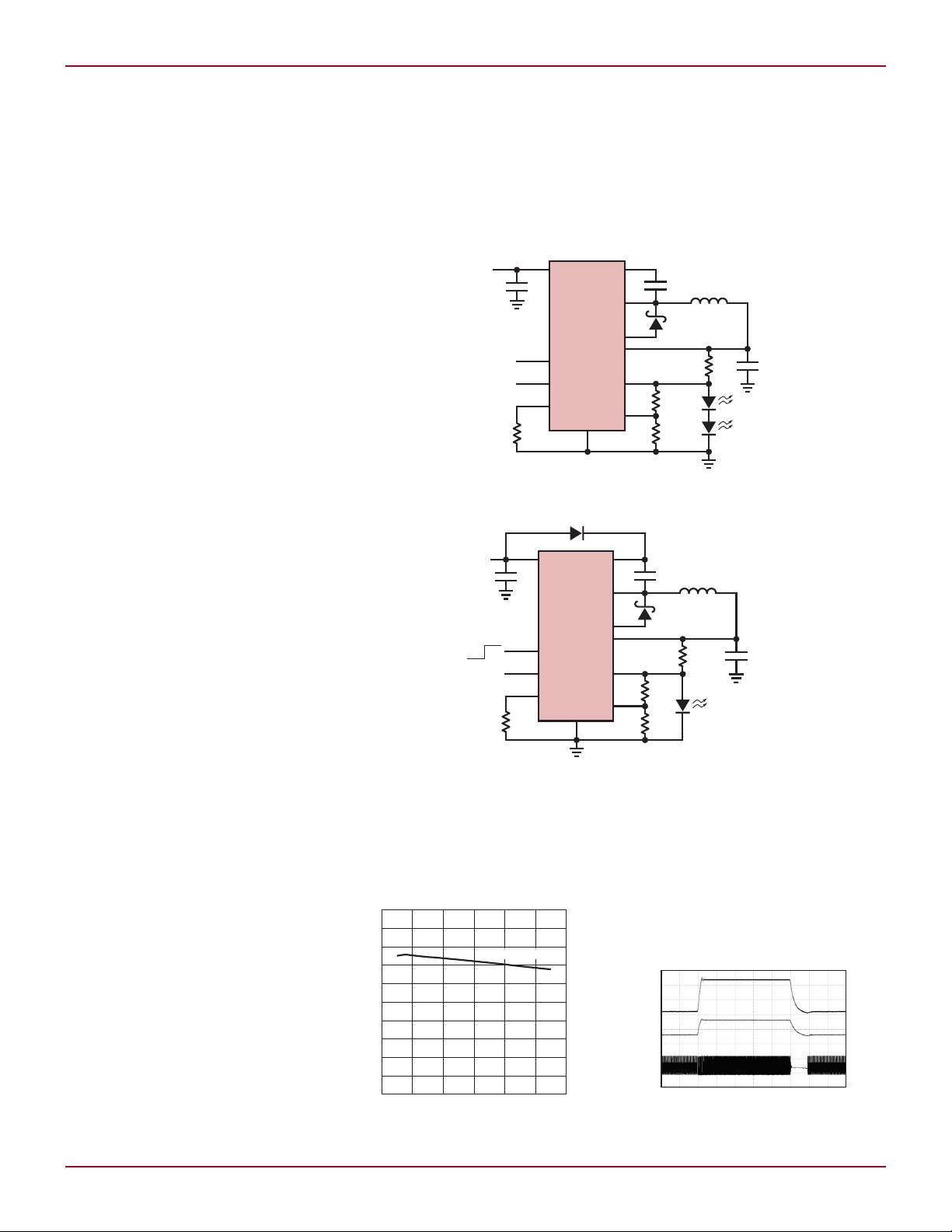
Figure 1. Two red LED application with no external boost diode
Figure 2. Single red LED application with external boost diode to V
IN
Simple 2-Level
Current Control
The LT3592 uses a single external
current sense resistor between the
CAP and OUT pins to set its two
output current levels, which have a
10:1 ratio. In bright mode, an internal
amplifier regulates the voltage difference between CAP and OUT to 200mV.
In dim mode, the voltage is regulated
to 20mV. Using a 0.4Ω current sense
resistor results in a bright current of
500mA and a DIM current of 50mA.
Switching between the high and low
current levels couldn’t be easier—bring
the BRIGHT pin above 1.4V for high
current, and below 0.3V for low current. The bright current level can be
as high as 500mA.
34
34
The output voltage of the LT3592
can be as high as 20V, but the part is
also designed to work well with single
red LEDs, which can have forward voltages below 2V at reasonable current
Figure 3. Efficiency for Figure 1
levels. The operating frequency can
be set anywhere between 400kHz and
2.2MHz using a single resistor from the
RT pin to ground. Set a lower operating frequency for the best efficiency,
and a higher frequency for smaller
filter components and overall solution
size. The LT3592 also incorporates an
Figure 4. Switching between dim (50mA) and
bright (500mA) modes with 4.7µF output cap
Linear Technology Magazine • June 2008
Page 2
internal Schottky diode between CAP
4.7µH
31.6k
4.7µF
1µF
0.4Ω
10k
48.7k
2.2MHz
0.1µF
MBRA140
V
IN
SHDN
BRIGHT
R
T
BOOST
SW
DA
CAP
OUT
V
FB
LT3592
GND
V
IN
8V TO 32V
5V
ON
+
–
R5
49.9Ω
3.3V 3.3V
R3
10Ω
R4
10Ω
R7
49.9Ω
R8
49.9Ω
R2
1k
V
OCM
R1
1.21k
3.3V
R6
49.9Ω
1/2
LTC6420-20
1/2
LTC6420-20
C2
12pF
V
IN
C5
12pF
C3
12pF
C1
0.1µF
C4
0.1µF
LTC2208
–3dB FILTER BANDWIDTH = 120MHz
and BOOST, which saves an external
component for applications with two
or more series LEDs (see Figure 2 for
a single LED solution).
Rugged Solution for
Tough Environments
In addition to an internal switch current limit circuit, the LT3592 includes
a catch diode current sense limit function that protects the circuit during
start-up at high input voltages. Simply
connect the anode of the Schottky
catch diode to the DA pin, and the
LT3592 automatically reduces the
oscillator frequency when the catch
diode current is higher than 1A. The
lower operating frequency prevents the
inductor current from ramping up in
an uncontrolled fashion and allows
the switch current limit to be effective
by avoiding minimum on time restrictions. The LT3592 also automatically
reduces its operating frequency if the
LED string shorts out, minimizing
power dissipation in the part.
The SHDN and BRIGHT pins are as
rugged as the VIN pin and can with-
Figure 5. A 5V power supply with a 500mA current limit
stand up to 36V, so they can be tied to
the input voltage. Nevertheless, both
pins have low voltage thresholds that
allow them to be directly interfaced to
low voltage microcontrollers.
The LT3592 is not only useful
for LED applications. It has a fully
functional voltage control loop, and
the current loop can be used as an
accurate current clamp for voltage
output applications. The voltage loop is
also useful as a voltage clamp in case
of an open LED fault. The transition
between voltage and current control
is stable and seamless.
DESIGN IDEAS L
Conclusion
The LT3592 makes 2-state bright/dim
LED control simple and rugged. It is an
ideal solution for applications such as
automotive brake lights and flashing
warning lights in industrial systems.
Accurate control of the current levels
makes LED brightness consistent
across units in a given application
regardless of varying LED forward
voltage characteristics. Switching
between the two current levels can
be accomplished with either very
low or very high voltage level digital
signals.
L
LTC6420, continued from page 33
ADC close to full scale, without driving the demodulator so hard that it
causes excessive distortion, you need
to insert some gain between the demodulator output and the ADC input.
In Figure 1, the LTC6421-20 provides
this gain, while the tight matching
between its two channels contributes
Linear Technology Magazine • June 2008
Figure 2. Connecting the two channels of the LTC6420-20 in parallel reduces the noise floor
a negligible amount of gain or phase
error. The bandwidth and linearity of the LTC6421-20 ensures that
14-bit linearity (distortion less than
–84dBc) is maintained to 50MHz and
beyond, an important design criteria
in digital-predistortion (DPD) circuits
or wideband receivers.
Paralleling Two Drivers to
Lower the Noise Floor
In applications with only one ADC, you
can hook-up the two channels of the
dual amplifier in parallel, as shown
in Figure 2. The main benefit of doing
so is a reduction in noise, because
the random noise contributions of
each channel get averaged out. For
example, input noise density (with
inputs shorted) drops from 2.2nV/√Hz
to 1.5nV/√Hz, a 3dB improvement in
SNR if the driver were the dominant
noise source.
Conclusion
The LTC6420 features two high speed
differential amplifiers in a small 3mm
× 4mm QFN package, with guaranteed
tight matching specs between the two
channels. It is ideal for driving high
frequency signals into dual ADCs,
especially when board space is limited
or when the magnitude and phase
relationship between the signals must
be preserved.
L
3535
 Loading...