

Linear Technology LT3591EDDB, LT3591 Datasheet
LT3591
1
3591f
■
Cellular Phones
■
PDAs, Handheld Computers
■
Digital Cameras
■
MP3 Players
■
GPS Receivers
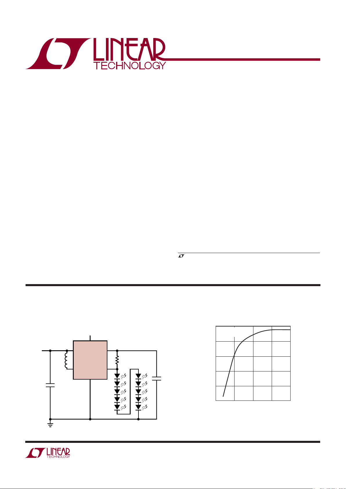
TYPICAL APPLICATION
FEATURES
APPLICATIONS
DESCRIPTION
White LED Driver with
Integrated Schottky in
3mm × 2mm DFN
The LT®3591 is a fi xed frequency step-up DC/DC converter
specifi cally designed to drive up to ten white LEDs in series
from a Li-Ion cell. Series connection of the LEDs provides
identical LED currents resulting in uniform brightness
and eliminating the need for ballast resistors. The device
features a unique high side LED current sense that enables
the part to function as a “one wire current source;” one
side of the LED string can be returned to ground anywhere,
allowing a simpler one wire LED connection. Traditional
LED drivers use a grounded resistor to sense LED current,
requiring a 2-wire connection to the LED string.
The high switching frequency allows the use of tiny inductors and capacitors. A single pin performs both shutdown
and accurate LED dimming control. Few external components are needed: open-LED protection and the Schottky
diode are all contained inside a low profi le 3mm × 2mm
DFN package.
Li-Ion Driver for Ten White LEDs
■
Drives Up to Ten White LEDs from a 3V Supply
■
High Side Sense Allows “One Wire Current Source”
■
Internal Schottky Diode
■
One Pin Dimming and Shutdown
■
80:1 True Color PWMTM Dimming Range
■
42V Open LED Protection
■
1MHz Switching Frequency
■
±5% Reference Accuracy
■
VIN Range: 2.5V to 12V
■
Requires Only 2.2µF Output Capacitor
■
Low Profi le 8-Lead DFN Package
(3mm × 2mm × 0.75mm)
Conversion Effi ciency
CTRL
V
IN
22µH
V
IN
3V TO 5V
R
SENSE
10Ω
3591 TA01a
LT3591
SHUTDOWN AND
DIMMING CONTROL
SW
CAP
LED
GND
2.2µF
1µF
LED CURRENT (mA)
0
EFFICIENCY (%)
60
20
3591 TA01b
5
10
15
80
70
55
65
75
VIN = 3.6V
10 LEDs
, LT, LTC and LTM are registered trademarks of Linear Technology Corporation.
True Color PWM is a trademark of Linear Technology Corporation. All other trademarks are
the property of their respective owners.
LT3591
2
3591f
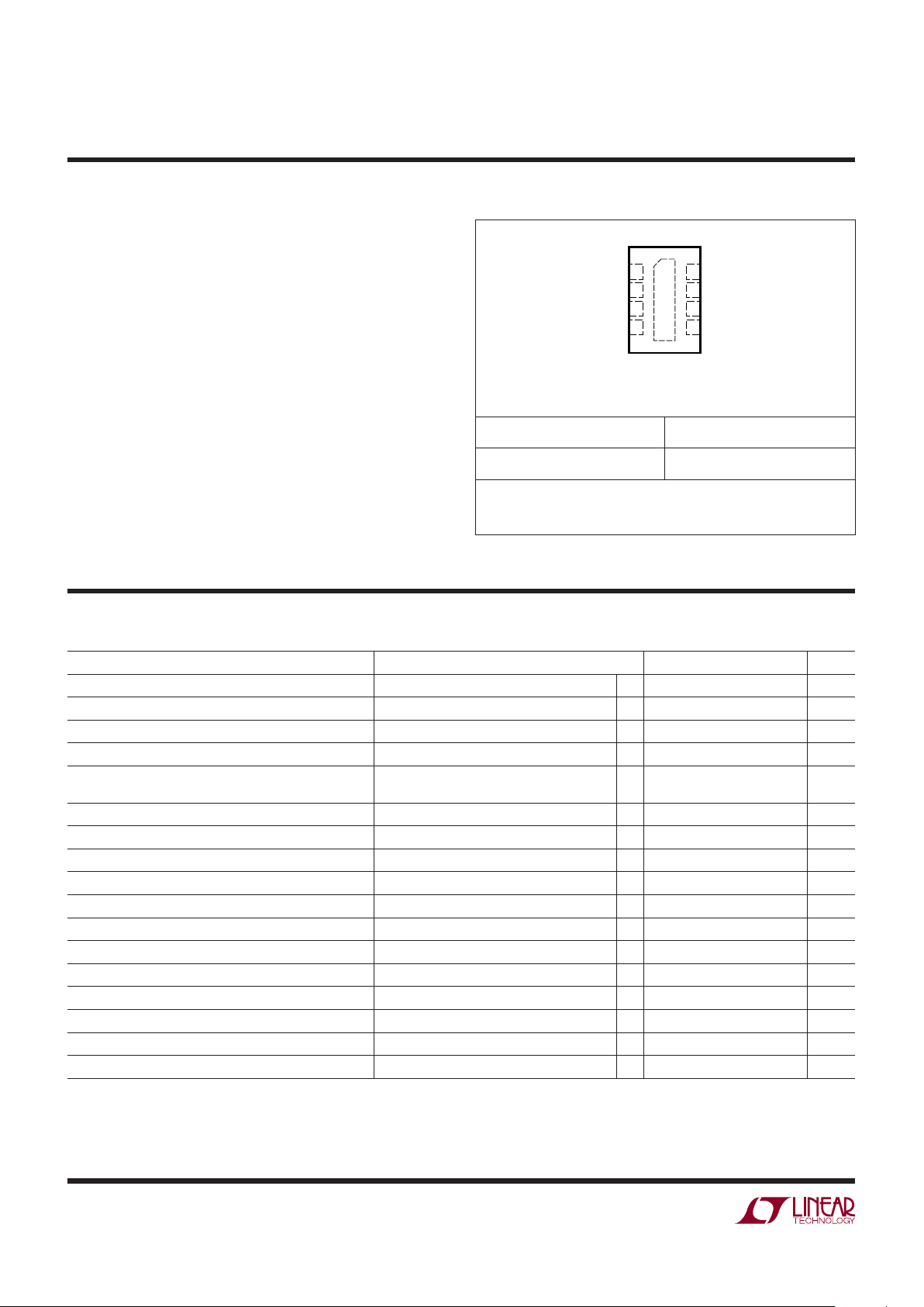
PACKAGE/ORDER INFORMATION
ELECTRICAL CHARACTERISTICS
ABSOLUTE MAXIMUM RATINGS
Input Voltage (VIN) ................................................... 12V
CTRL Voltage ........................................................... 12V
SW Voltage .............................................................. 45V
CAP Voltage ............................................................. 45V
LED Voltage ............................................................. 45V
Operating Junction Temperature Range
(Note 2) ...............................................–40°C to 85°C
Maximum Junction Temperature ........................ 125°C
Storage Temperature Range ...................–65°C to 150°C
(Note 1)
Note 1: Stresses beyond those listed under Absolute Maximum Ratings
may cause permanent damage to the device. Exposure to any Absolute
Maximum Rating condition for extended periods may affect device
reliability and lifetime.
PARAMETER CONDITIONS MIN TYP MAX UNITS
Minimum Operating Voltage
2.5 V
LED Current Sense Voltage (V
CAP
– V
LED
)V
CAP
= 24V, ISW = 300mA
●
190 200 210 mV
CAP Pin Bias Current V
CAP
= 36V, V
LED
= 35.8V
40 80 µA
LED Pin Bias Current V
CAP
= 36V, V
LED
= 35.8V 20 40 µA
Supply Current V
CAP
= 24V, V
LED
= 23V
CTRL = 0V
4
9
5
11
mA
µA
Switching Frequency 0.75 1 1.2 MHz
Maximum Duty Cycle 92 94 %
Switch Current Limit
●
500 800 mA
Switch V
CESAT
ISW = 300mA 200 mV
Switch Leakage Current V
SW
= 24V 0.1 5 µA
V
CTRL
for Full LED Current V
CAP
= 44V
●
1.5 V
V
CTRL
to Shut Down IC 50 mV
V
CTRL
to Turn On IC
●
100 mV
CTRL Pin Bias Current 100 nA
CAP Pin Overvoltage Protection
●
40 42 44 V
Schottky Forward Drop I
SCHOTTKY
= 200mA 0.8 V
Schottky Leakage Current V
R
= 30V 4 µA
TOP VIEW
9
DDB PACKAGE
8-LEAD (3mm × 2mm) PLASTIC DFN
5
6
7
8
4
3
2
1V
IN
GND
NC
SW
CTRL
LED
NC
CAP
T
JMAX
= 125°C, θJA = 76°C/W
EXPOSED PAD (PIN 9) SHOULD BE CONNECTED TO PCB GROUND
ORDER PART NUMBER DDB PART MARKING
LT3591EDDB LCPG
Order Options Tape and Reel: Add #TR
Lead Free: Add #PBF Lead Free Tape and Reel: Add #TRPBF
Lead Free Part Marking: http://www.linear.com/leadfree/
Consult LTC Marketing for parts specifi ed with wider operating temperature ranges.
The
●
denotes the specifi cations which apply over the full operating
temperature range, otherwise specifi cations are at T
A
= 25°C. VIN = 3V, V
CTRL
= 3V, unless otherwise specifi ed.
Note 2: The LT3591E is guaranteed to meet performance specifi cations
from 0°C to 85°C operating junction temperature range. Specifi cations
over the –40°C to 85°C operating junction temperature range are assured
by design, characterization and correlation with statistical process controls.
LT3591
3
3591f
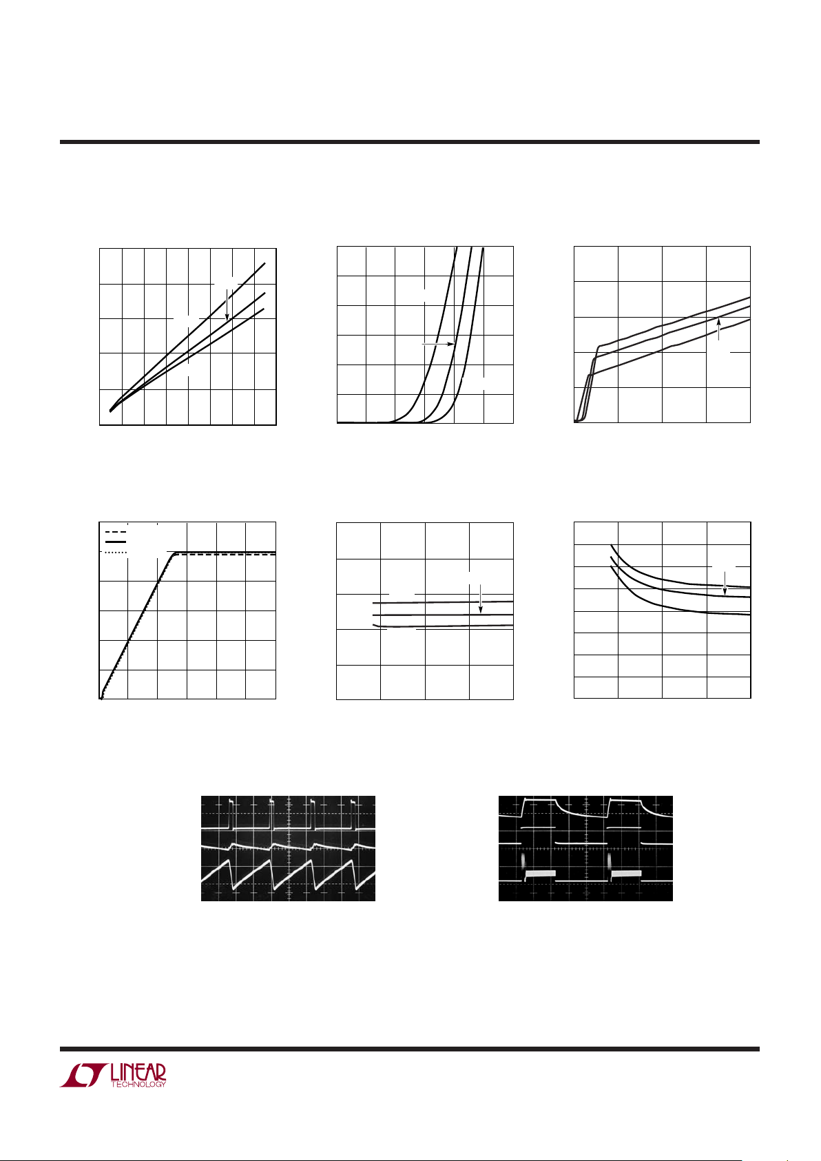
TYPICAL PERFORMANCE CHARACTERISTICS
Switch Saturation Voltage
(V
CESAT
)
Schottky Forward Voltage Drop
Shutdown Current (V
CTRL
= 0V)
Sense Voltage (V
CAP
– V
LED
)
vs V
CTRL
Open-Circuit Output
Clamp Voltage
Input Current in Output
Open Circuit
Switching Waveform
Transient Response
SWITCH CURRENT (mA)
0
500
400
300
200
100
0
300 600
3591 G01
100 200
400 800700
500
SWITCH SATURATION VOLTAGE (mV)
–50°C
125°C
25°C
SCHOTTKY FORWARD DROP (mV)
SCHOTTKY FORWARD CURRENT (mA)
200
300
3591 G02
100
0
600
500
400
0 200 400 600 800
1000 1200
–50°C
125°C
25°C
VIN (V)
0
SHUTDOWN CURRENT (µA)
9
12
15
12
3591 G03
6
3
0
3
6
9
–50°C
125°C
25°C
V
CTRL
(mV)
SENSE VOLTAGE (mV)
80
120
3591 G04
40
0
240
200
160
0 500 1000 1500 2000 2500 3000
–50°C
25°C
125°C
VIN (V)
0
OUTPUT CLAMP VOLTAGE (V)
42
43
12
3591 G05
41
40
3
6
9
45
44
–50°C
125°C
25°C
VIN (V)
0
INPUT CURRENT (mA)
36 912
3591 G06
–50°C
125°C
4
5
6
3
2
0
1
8
7
25°C
V
SW
20V/DIV
V
CAP
50mV/DIV
I
L
200mA/DIV
V
IN
= 3.6V
FRONT PAGE
APPLICATION CIRCUIT
500ms/DIV
3591 G07
V
CTRL
5V/DIV
V
CAP
5V/DIV
I
L
500mA/DIV
V
IN
= 3.6V
FRONT PAGE
APPLICATION CIRCUIT
1ms/DIV
3591 G08
TA = 25°C, unless otherwise specifi ed.
LT3591
4
3591f
VIN (V)
0
0
QUIESCENT CURRENT (mA)
1
2
3
4
5
6
36 912
3591 G09
–50°C
125°C
25°C
TEMPERATURE (°C)
0
CURRENT LIMIT (mA)
400
1000
3591 G10
200
600
800
–50 –25 0 25 50 75 100 125
–50 25 75
–25 0
50 100 125
TEMPERATURE (°C)
0
SCHOTTKY LEAKAGE CURRENT (µA)
3
6
9
12
15
3591 G11
VR = 10V
V
R
= 16V
V
R
= 20V
TEMPERATURE (°C)
–50 –25
40
OUTPUT CLAMP VOLTAGE (V)
42
45
0
50
75
3591 G12
41
44
43
25
100
125
TEMPERATURE (°C)
–50
INPUT CURRENT (mA)
25 75
3591 G13
–25 0
50 100 125
VIN = 3V
4
5
6
3
2
0
1
8
7
TEMPERATURE (°C)
–50
SWITCHING FREQUENCY (kHz)
25 75
3591 G14
–25 0
50 100 125
1000
1050
1100
950
900
750
800
850
1200
1150
TEMPERATURE (°C)
–50
MAXIMUM DUTY CYCLE (%)
25 75
3591 G15
–25 0
50 100 125
98
96
94
90
92
100
V
CAP
(V)
5
SENSE VOLTAGE (mV)
20 30
3591 G16
10 15
25 35
204
200
196
188
192
208
–50°C
125°C
25°C
TEMPERATURE (°C)
–50 –25
188
SENSE VOLTAGE (mV)
196
208
0
50
75
3591 G17
192
204
200
25
100
125
TYPICAL PERFORMANCE CHARACTERISTICS
Quiescent Current
(V
CTRL
= 3V) Current Limit vs Temperature
Schottky Leakage Current
vs Temperature
Open-Circuit Output Clamp
Voltage vs Temperature
Input Current in Output Open
Circuit vs Temperature
Switching Frequency
vs Temperature
Maximum Duty Cycle
vs Temperature
Sense Voltage (V
CAP
– V
LED
)
vs V
CAP
Sense Voltage (V
CAP
– V
LED
)
vs Temperature
T
A
= 25°C, unless otherwise specifi ed.
LT3591
5
3591f
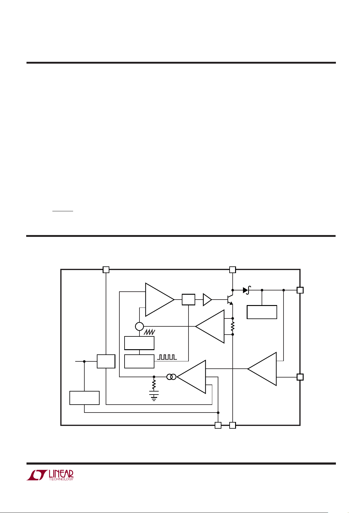
BLOCK DIAGRAM
PIN FUNCTIONS
VIN (Pin 1): Input Supply Pin. Must be locally bypassed.
GND (Pin 2): Ground Pin. Should be tied directly to local
ground plane.
SW (Pin 4): Switch Pin. Minimize trace area at this pin to
minimize EMI. Connect the inductor at this pin.
CAP (Pin 5): Output of the Driver. This pin is connected
to the cathode of internal Schottky. Connect the output
capacitor to this pin and the sense resistor from this pin
to the LED pin.
LED (Pin 7): Connection Point for the Anode of the First
LED and the Sense Resistor. The LED current can be
programmed by :
I
mV
R
LED
SENSE
=
200
CTRL (Pin 8): Dimming and Shutdown Pin. Connect this
pin below 50mV to disable the driver. As the pin voltage
is ramped from 0V to 1.5V, the LED current ramps from
0 to I
LED
( = 200mV/R
SENSE
). The CTRL pin must not be
left fl oating.
Exposed Pad (Pin 9): Ground. The Exposed Pad must
be soldered to PCB ground to achieve the rated thermal
performance.
4
–
+
–
+
R
SW
CAP
1
V
IN
Q
S
DRIVER
Σ
OVERVOLTAGE
PROTECTION
RAMP
GENERATOR
OSCILLATOR
V
REF
1.25V
START-UP
CONTROL
SHDN
Q1
R
–
+
+
5
LED
3591 F01
CTRL GND
7
82
–
+
A = 6.25
A1
R
C
C
C
A2
A3
PWM
COMP
Figure 1. Block Diagram
 Loading...