


L DESIGN IDEAS
BATTERY VOLTAGE (V)
2.7
500
600
700
3.9
400
300
3.0 3.3 3.6 4.2
200
100
0
CHARGE CURRENT (mA)
V
BUS
= 5V
R
PROG
= 1k
R
CLPROG
= 3k
5x USB SETTING,
BATTERY CHARGER SET FOR 1A
Complete Power Solution for Digital
Cameras and Other Complex
Compact Portable Applications
Introduction
Digital cameras, portable GPS systems,
MP3 players and other feature-rich
mobile devices have complicated
power requirements. In these complex
devices, the flow of power must be
carefully managed between a number of specialized sources and loads,
including charging/discharging the
battery, current-limited USB power
and a set of multivoltage power supply rails, including negative rails for
CCDs or LCDs. The supply rails must
be sequenced and tracked and faults
must be handled cleanly and communicated to a microcontroller.
When these requirements are
added together, the task of squeezing
an efficient and robust power system
into a handheld device can seem near
impossible. Linear Technology solves
this problem with a family of devices
called PMICs (Power Management Integrated Circuits) that greatly simplify
the design of complex rechargeable
battery power systems.
Some Linear Technology PMICs
use a switching PowerPath controller
topology with the unique Bat-Track
feature, which allows charge currents
above the USB limit (see Figure 1) for
faster battery charging. The power
solution for digital cameras presented
34
34
Figure 1. Battery charge current
vs battery voltage
The LTC3586 implements
Linear Technology’s unique
Bat-Track™ technology,
which can use more power
from a USB source than
traditional linear chargers,
resulting in faster charging.
here takes advantage of this and other
powerful PMIC features.
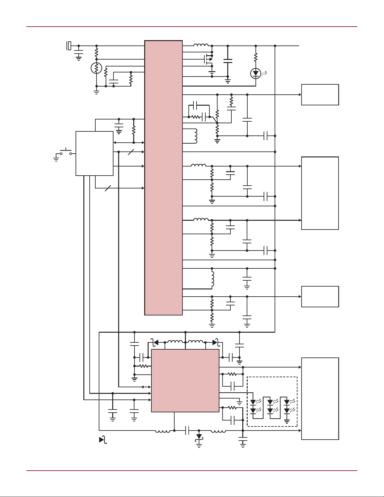
Complete Digital Camera
Power System
Figure 2 shows a complete digital
camera power solution using the
LTC3586 PMIC as the power traffic
control center. Its 4mm × 6mm QFN
package includes a USB PowerPath
manager, a battery charger, plus a
boost DC/DC converter, a buck-boost
and two buck converters. The LT3587
in a 3mm × 3mm package is used to
drive a CCD and an LED backlight
for an LCD screen with a high voltage
monolithic inverter and dual boost
converter.
Switching PowerPath
Controller Maximizes
Available Power
The LTC3586 implements Linear
Technology’s unique Bat-T rack™
technology, which maximizes the use
of available power from a USB source
for either providing current to the
load or charging the battery at rates
greater than achievable from linear
chargers.
The switching PowerPath controller maintains accurate control of the
average input current for USB applications. The average level of input
current is controlled by the state
of two digital inputs and can be set
by Brian Shaffer
to 100mA, 500mA, 1A or suspend
(500µA). The switching PowerPath
controller is highly efficient, which
results in battery charge currents of
well over 600mA from a 500mA USB
source (Figure 1).
The battery charging efficiency is
between 85% and 90% for the entire
battery voltage range. In contrast,
the efficiency of a traditional linear
charger falls as low as 57%, generating
the losses as heat. See Figure 3 for a
graph of the battery charger efficiency
as a function of battery voltage.
Instant-On Operation
The LTC3586 also features instant-on
operation, which allows the camera to
function immediately when external
power is applied even if the battery
voltage is below the system cutoff
voltage. This is achieved by generating
a separate voltage rail, V
is decoupled from the battery voltage when the battery is below 3.3V.
When external power is applied, the
PowerPath controller prioritizes load
current over battery charge current
and regulates V
to 3.6V, enabling
OUT
the system to operate immediately
upon the application of external power.
The instant-on feature is important in
camera applications because impor tant moments do not wait for batteries
to charge.
Fault Handling
The FAULT signals on both of these
devices are designed to work together
for seamless fault handling. By making
the fault signals both an input and
an output, the two chips can communicate fault events to each other.
If either of the devices has a fault then
all the outputs turn off, protecting
the system and battery from damage.
The enable lines and the fault signal
Linear Technology Magazine • September 2008
, which
OUT
+
MP1
C2
22µF
Li-Ion
510Ω
324k
121k
105k
RED
3.3V
1A
1.8V
400mA
MICROPROCESSOR
1.6V
400mA
5V
800mA
15V
50mA
BACKLIGHT LEDs
–8V
100mA
L1
3.3µH
L2
2.2µH
SW
V
BUS
T
NTC
PROG
CLPROG
100k
LTC3586
V
OUT3
V
C3
3.3V, 20mA
FB3
SWCD3
SWAB3
LDO3V3
I
LIM
MODE
FAULT
4
EN
V
OUT
BAT
GND
CHRG
GATE
2.2µF
330pF
33pF
10pF
15k
1µF
1µF
22µF
V
IN3
10pF1.02M
C1, C2: TDK C2012X5R0J226M
L1: COILCRAFT LPS4018-332LM
L2, L5: TOKO 1098AS-2R2M
L3, L4: TOKO 1098AS-4R7M
MP1: SILICONIX Si2333
806k
10k
L3
4.7µH
SW2
FB2
I/O/MEMORY
CORE
10µF
V
IN2
10pF
10pF
806k
806k
L4
4.7µH
L5
2.2µH
SW1
FB1
10µF
88.7k
16.9k
V
IN1
SW4
V
OUT4
FB4
V
IN4
SYSTEM RAIL/
I/O
AUDIO/
MOTOR DRIVE
CCD
2.94k
2k
0.1µF
C1
22µF
USB/WALL
4.5V TO 5.5V
1µF
PUSHBUTTON
MICROCONTROLLER
2
10µF
22µF
100nF100nF
15µH
10µH
VOUT3
CAP3
VFB3
IFB3
SW2
FB2
GND
CAP1
FB1
VOUT1
LT3587
EN/SS1
EN/SS3
SW3 SW1VIN
10µF
2.2µF
15µH 15µH
CCD POSITIVE
CCD NEGATIVE
8.06k
1µF
LED DRIVER
20mA, UP TO 6 LEDS
2.2µF
1M
1M
22µF
V
OUT
2.7pF
6.8pF
FLT
1µF
= IR05H40CSPTR
DESIGN IDEAS L
Linear Technology Magazine • September 2008
Figure 2. Complete power solution for portable cameras
3535

L DESIGN IDEAS
BATTERY VOLTAGE (V)
2.7
EFFICIENCY (%)
80
90
3.9
70
60
3
3.3
3.5
4.2
100
R
CLPROG
= 3.01K
R
PROG
= 1K
I
VOUT
= 0mA
5x CHARGING EFFICIENCY
1x CHARGING EFFICIENCY
10µH
VOUT3
CAP3
IFB3
LT3587
8.06k
R
IFB3
EN/SS3
SW3
VIN
1µF
V
VIN
2.5V TO 5V
V
DAC-OUT
DAC
LTC2630
PWM
FREQ
2.5V
0V
MN1
Si1304BDL
IR05H40CSPTR
Figure 3. Battery charging efficiency vs
battery voltage with no external load
(P
should be pulled-up to the same voltage. In Figure 2 the LDO3V3 regulator
is used as the pull-up voltage for the
FAULT signal and the power supply
for the low power microcontroller
used to process pushbutton events
and sequence the power supplies.
The FAULT pin also acts as an input
and hence, must be high before any
outputs are enabled.
Compact LED Driver
The LT3587 LED driver is designed
to drive up to six LEDs with average
LED currents between 20mA and 1µA.
When the LT3587’s V
a current regulated LED driver, the
V
FB3
protection function. By connecting a
resistor between V
device limits the maximum allowable
output voltage on V
is extremely important in LED applications because without it the client
device may be damaged if one of the
LEDs were to open; in such a case,
the output would continue to rise as
)
BAT/PBUS
is used as
OUT3
pin can be used as an overvoltage
and V
OUT
. This feature
OUT3
FB3
the
Figure 4. Six white LED driver with PWM and analog dimming
the current regulation loop increases
voltage in an attempt to regulate the
current.
The integrated LED driver in the
LT3587 is capable of accepting a direct
PWM dimming signal into its enable
input (EN/SS3) and/or accommodates
analog dimming via an external DAC.
See Figure 4 for a partial application
circuit showing the LED driver with
direct PWM and analog dimming.
LEDs can change color when the
current through them changes, but
PWM dimming maintains color consistency over the dimming range, as the
ON part of the PWM cycle is always the
same current. In PWM dimming, the
brightness of the LEDs is a function of
average current, adjusted by changing
the duty cycle of the PWM signal. In
analog dimming, the constant current
through the LEDs is adjusted, which
causes variations in color.
The LT3587 accepts PWM signals
with frequencies over 60Hz to assure
flicker-free operation. High PWM frequencies are achievable because of
the internal disconnect FET between
CAP3 and V
. This FET ensures
OUT3
that CAP3 maintains its steady-state
value while the PWM signal is low,
resulting in minimal startup delays.
For a 100Hz PWM dimming signal and
allowing for 10% deviation from linearity at the lowest duty cycle, the LT3587
allows for a dimming ratio of 30:1. If
the maximum amount of adjustment
range is desired, an external DAC,
such as the LTC2630, can be used to
feed an adjustment voltage onto the
IFB3 resistor, creating an LED current
range of 20,000:1.
Conclusion
Two highly integrated devices, the
LTC3586 and LT3587 can be combined
to create a complete USB compatible
power solution for portable cameras
and other feature-rich portable devices. The solution is robust, high
performance and compact, with efficient battery charging, instant-on
capability and LED protection.
L
LTC3851, continued from page 17
protects against insufficient turn-on
voltage for the top MOSFET.
3.3V/15A Regulator with
DCR Sensing
Figure 2 shows a 400kHz, 3.3V output
regulator using DCR current sensing.
The DC resistance of the inductor is
used as the current sense element,
eliminating the need for a discrete
sense resistor and thus maximizing
efficiency. Figure 3 shows a plot of the
36
36
efficiency vs load for all three modes
of operation with an input voltage of
12V.
1.5V/15A Regulator
Synchronized at 350kHz
Figure 4 illustrates a 1.5V output
regulator that is synchronized to
an external clock. The loop filter
components connected to the FREQ/
PLLFLTR pin are optimized to achieve
a jitter free oscillator frequency and
reduced lock time.
Conclusion
The LTC3851 combines high performance, ease of use and a comprehensive
feature set in a 3mm × 3mm 16-pin
package. DCR current sensing and
Burst Mode® operation keep efficiency
high. With a broad 4V to 38V input
range, strong MOSFET drivers, low
minimum on-time and tracking, the
LTC3851 is ideal for automotive electronics, server farms, datacom and
telecom power supply systems and
industrial equipment.
Linear Technology Magazine • September 2008
L
 Loading...