

L DESIGN FEATURES
LOAD CURRENT (mA)
0.1
35
EFFICIENCY (%)
POWER LOSS (mW)
45
350
300
250
200
150
100
50
0
55
65
75
85
95
1 10 100
V
OUTP
V
OUTN
LT3582
V
IN
SWP
CAPP
V
NEG
–12V
85mA
CAPP
V
PP
SDA
SCL
CA
GND
SWN
SWN
V
OUTN
I2C
INTERFACE
V
OUTP
SHDN
INPUT
4.5V TO 5.5V
V
POS
12V
80mA
L1
6.8µH
D1
C2
4.7µF
C6
10nF
C5
10nF
RAMPNRAMPP
C3
C1
4.7µF
C4 1µF
D2
L2 6.8µH
OPTIONAL ON
LT3582-12
REG0/OTP0 = B0h
REG1/OTP1 = D8h
REG2/OTP2 = 03h
D1-D2: DIODES INC. B0540WS-7
L1-L2: COILCRAFT XPL2010-682
C1: 4.7µF, 6.3V, X5R, 0805
C2: 4.7µF, 16V, X5R, 0805
C3: 1s 4.7µF OR 2s 4.7µF OR 10µF
16V, X5R, 0805
C4: 1µF, 16V, X5R, 0603
C5-C6: 10nF, 0603
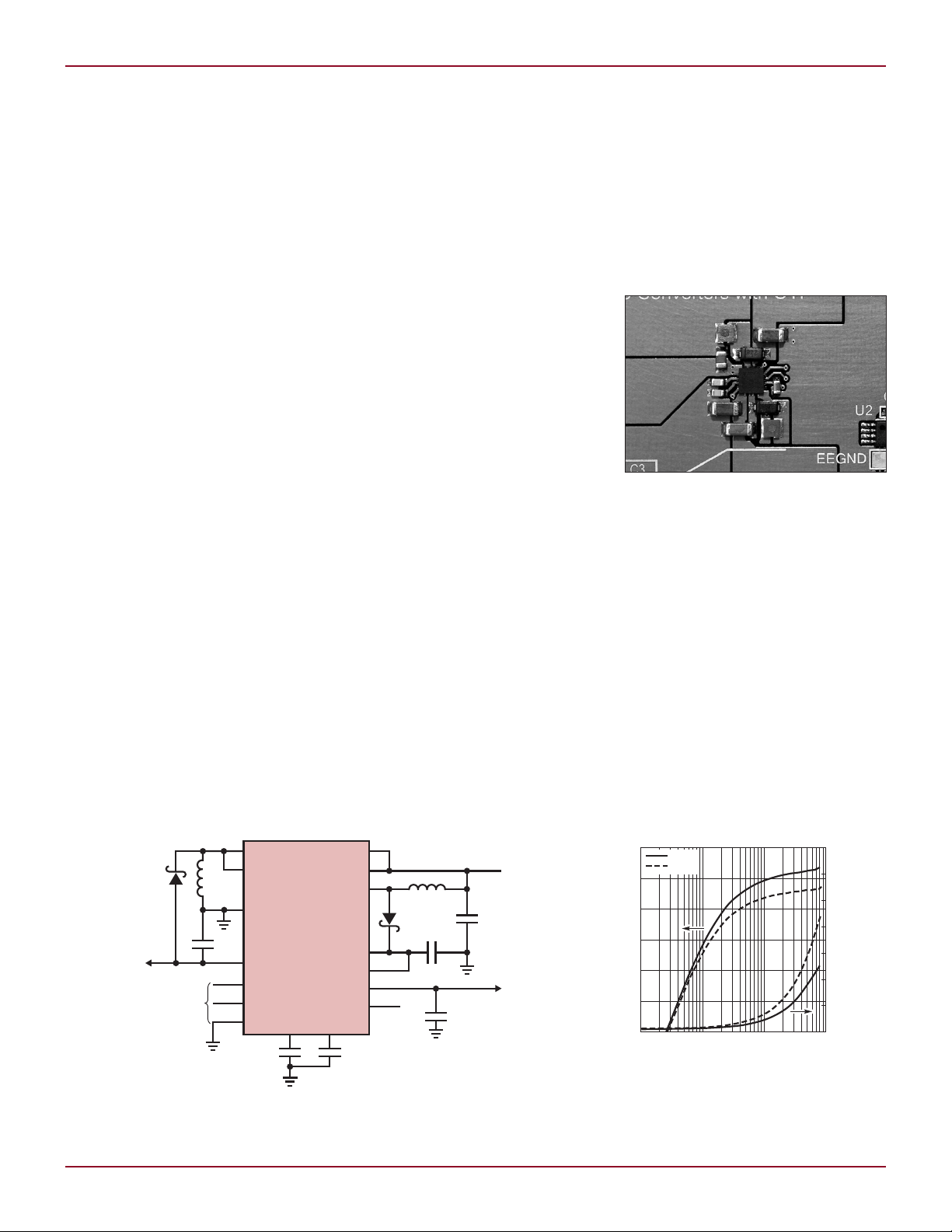
Space-Saving, Dual Output
DC/DC Converter Yields Plus/Minus
Voltage Outputs with (Optional)
I2C Programming
Introduction
There are many applications that require both positive and negative DC
voltages generated from a single input
supply. The LT3582 is a highly integrated dual switching regulator that
produces positive and negative voltages for AMOLEDs, CCDs, op amps, and
general ±5V and ±12V supplies. The
LT3582 uses a novel control scheme
resulting in low output voltage ripple
and high conversion efficiency over a
wide load current range. The total solution size is very small due to the tiny
3mm × 3mm 16-pin QFN package, integrated feedback resistors, integrated
loop compensation networks and the
single-inductor negative output topology (see Figure 1).
The LT3582-5 and LT3582-12 are
factory configured for accurate ±5V
and ±12V outputs respectively, making
it easy to squeeze a high performance
solution into a small space. For other
voltage combinations, the LT3582
offers I2C digitally programmable out-
puts of 3.2V to 12.775V and –1.2V to
–13.95V that can be made permanent
with on-chip OTP (One-Time-Programming) memory. The input supply range
is 2.55V to 5.5V and switch current
limits are 350mA and 600mA for the
boost and inverting switches, respectively. In addition, the LT3582 features
power up sequencing with ramping
from ground to regulation, power down
discharging, positive output disconnect and soft-start.
Accurate Output Voltages
without External Feedback
Resistors
The LT3582 series uses integrated
feedback resistors to select the output
voltages. The LT3582-5 and LT358212 are pre-configured at the factory
for ±5V and ±12V outputs with ±1.5%
accuracy or better. The LT3582 allows
other output voltages to be configured
using the I2C interface. There are
nine bits to configure the positive
output voltage from 3.2V to 12.775V
in 25mV steps and another eight bits
to configure the negative output voltage from –1.2V to –13.95V in 50mV
steps. Default settings can be stored
by Mathew Wich
Figure 1. Dual output supplies
in a small board footprint
in One-Time-Programmable memory
and, if left unlocked, the voltages can
be subsequently changed on the fly
using the I2C interface.
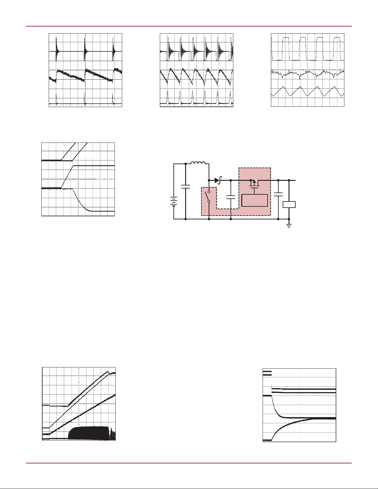
Great Performance
Includes Low Ripple and
High Efficiency Across
the Load Range
The LT3582 is among several novel
parts from Linear Technology that
modulate peak switch current and
switch off time to reduce ripple and
improve light load efficiency (also see
the LT3494, LT3495, LT8410 and
22
Figure 2. ±12V supplies from a single 5V input
Linear Technology Magazine • June 2009
DESIGN FEATURES L
L1
D1
SWP
C1
V
OUTP
C3
V
IN
C2
CAPP
LT3582
SERIES
DISCONNECT
CONTROL
LOAD
V
VOUTP
10mV/DIV
AC COUPLED
V
SWP
5V/DIV
I
L2
0.2A/DIV
5µs/DIV
CAPP
2V/DIV
I
L2
0.2A/DIV
V
RAMPP
0.2V/DIV
V
OUTP
2V/DIV
1ms/DIV
V
VOUTP
5V/DIV
V
VOUTN
5V/DIV
V
RAMPP
0.5V/DIV
V
RAMPN
0.5V/DIV
5ms/DIV
RAMPN
RAMPP
V
RAMPP
1V/DIV
V
RAMPN
1V/DIV
V
VOUTN
5V/DIV
V
VOUTP
5V/DIV
5ms/DIV
V
VOUTP
10mV/DIV
AC COUPLED
V
SWP
5V/DIV
I
L2
0.2A/DIV
200ns/DIV
V
VOUTP
10mV/DIV
AC COUPLED
V
SWP
5V/DIV
I
L2
0.2A/DIV
2µs/DIV
Figure 3. Switching waveforms at 1mA load
for the boost application shown in Figure 2
Figure 6. Power-Up Sequencing
(V
followed by V
OUTP
OUTN
)
LT8415). Under light load conditions,
the LT3582 chooses an optimum
combination of frequency and peak
switch current to improve efficiency
while moderating the output ripple.
Figures 3–5 show how the frequency
and peak inductor current vary from
light to heavy loads. At very light loads
(typically < 1mA), peak switching
currents are dramatically reduced to
further reduce ripple when frequencies
are in the audio band.
Figure 8. V
Linear Technology Magazine • June 2009
soft-start ramping from ground
OUTP
Figure 4. Switching waveforms at 10mA load
for the boost application shown in Figure 2
Figure 7. Output disconnect PMOS
Adjustable Power-Up
Sequencing and
Soft-Start Options
The LT3582 has digitally configurable
power-up sequencing that forces the
outputs to power up in one of four
ways:
q
V
ramps up first, followed by
OUTP
V
(shown in figure 6)
OUTN
q
V
ramps up first, followed by
OUTN
V
OUTP
q
both outputs ramp up
simultaneously
q
both outputs are disabled
The LT3582-5 and LT3582-12 are
factory configured for both outputs to
ramp up simultaneously.
The power-up ramp rates of the output voltages are also adjustable. Slowly
ramping the outputs (also known as
soft-start) reduces what would otherwise be high peak switching currents
during start-up. Without soft-start,
high start-up current is inherent in
switching regulators due to V
far from its final value. The regulator
tries to charge the output capacitors
OUT
Figure 5. Switching waveforms at 100mA load
for the boost application shown in Figure 2
as quickly as possible, which results
in large peak currents.
The output voltage ramp rates are
proportional to the ramp rates of the
RAMPP and RAMPN pin voltages. Upon
chip enable, a programmable current
(1µA, 2µA, 4µA or 8µA) linearly charges
capacitors (typically about 10nF)
connected to the RAMPP and RAMPN
pins. By varying the capacitor sizes
or charging currents, a wide range
of output voltage ramp rates can be
accommodated.
being
Figure 9. Power-down discharge waveforms
23
L DESIGN FEATURES
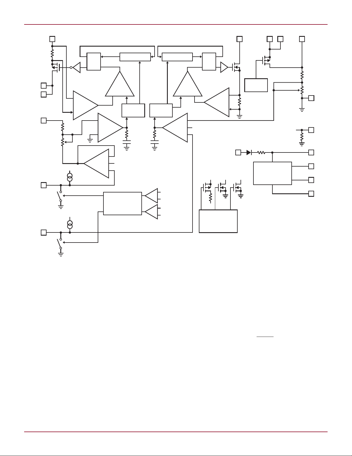
+
–
+
–
V
IN
SWN
SWN
FBN
VCN VCP
OTP
RAMPN
RAMPP
V
OUTN
CAPP
GND
SHDN
CHIP ENABLE
222k
V
PP
SCL
SDA
CA
OTP
SWP CAPP V
OUTP
–
+
–
+
+
–
–
+
–
+
+
2V
OTP ADJUST
OTP ADJUST
0.80V
0.75V
CAPP
V
OUTP
V
OUTN
V
IN
FBP
FBN
50mV
2V
OUTPUT SEQUENCING
BY OTP
I
PEAK TOFF
CONTROL
I
PEAK TOFF
CONTROL
Q S
Q R
QS
QR
VARIABLE DELAY VARIABLE DELAY
–
+
+
–
+
DISCONNECT
CONTROL
SERIAL INTERFACE,
LOGIC AND OTP
OUTPUT SEQUENCING
V
IN
0.80V
FBP
Output Disconnect and
Improved Efficiency
The LT3582 series has a PMOS output
disconnect switch connected between
CAPP and V
normal operation the switch is closed
(see Figure 7). During
OUTP
and current is limited to about 155mA
to help protect against output shorts.
During shutdown, the PMOS switch is
open providing up to 5V–5.5V of isolation between CAPP and V
cases this allows V
to ground.
In normal operation, the output
disconnect switch represents ~1.4Ω
of resistance in series with the output
leading to a 1%–2% efficiency loss under heavy load conditions. The CAPP
pin can be externally shorted to the
V
pin to eliminate the power loss
OUTP
in the switch and improve efficiency.
24
OUTP
to discharge
OUTP
. In most
Figure 10. LT3582 block diagram
Unique Ability to Ramp
Output Up From Ground
Smart control of the output disconnect PMOS also gives the LT3582 the
unique ability to generate a smooth
V
voltage ramp starting from
OUTP
ground and continuing all the way
up to regulation (see Figures 6 and 8).
This ability is not possible with typical
boost converters because the current
path from VIN through the inductor
(L1) and Schottky diode (D1) to the
output prevents it from starting at 0V
(see Figure 7).
The disconnect control circuitry in
the LT3582 allows V
ground when disabled. Once enabled,
the gate of the output disconnect
PMOS is precisely controlled such that
V
rises smoothly from ground up
OUTP
to regulation where the PMOS is fully
turned on to reduce power losses.
to discharge to
OUTP
Power Down Discharge Assist
The power down discharge feature assists in discharging the outputs after
shutdown (see Figure 9). This option
is factory enabled on the LT3582-5
and LT3582-12 and can be enabled
through the I2C interface in conjunction with the “both together” power-up
setting on the LT3582.
Upon SHDN falling and when
power -down discharge is enabled,
internal transistors activate to assist
in discharging the outputs toward
ground. After both outputs are within
~0.5V to ~1.5V of ground, the chip
powers down.
Digital Control and
One-Time Programming
The LT3582 series supports the Standard Mode I2C interface. Although
using this interface is not required
Linear Technology Magazine • June 2009

DESIGN FEATURES L
LOAD CURRENT (mA)
0.1
EFFICIENCY (%)
POWER LOSS (mW)
30
40
60
80
350
300
250
200
150
100
50
0
50
70
90
1 10 100
VIN = 3.3V
LT3582
V
IN
SWP
CAPP
V
NEG
–5V
90mA
CAPP
V
PP
SDA
SCL
CA
GND
SWN
SWN
V
OUTN
I2C
INTERFACE
V
OUTP
SHDN
INPUT
2.7V TO 4.2V
V
POS
4.6V
100mA
L1
1.5µH
D1
C2
10µF
C6
10nF
C5
10nF
RAMPNRAMPP
C3
10µF
C1
10µF
D2
C4 10µF
L2 1.5µH
REG0/OTP0 = 1Ch
REG1/OTP1 = 4Ch
REG2/OTP2 = 07h
D1-D2: PANASONIC M21D3800L LOW VF SCHOTTKY
L1-L2: TDK MLP3216S1R5L
C1-C4: TAIYO YUDEN JMK212BJ106MK, 6.3V, X5R 0805
C5-C6: 0402 X5R
VDS (V)
0.1
0.01
I
D
(A)
0.1
1
10
1 10 100
TA = 25°C
MULTIPLE PULSE
DUTY CYCLE = 0.2
DC
10s
100ms
10ms
1ms
1s
R
SET
(Ω)
1k
0
CURRENT LIMIT THRESHOLD VALUE (A)
0.5
1.0
1.5
2.0
2.5
10k 100k 1M 10M
for the LT3582-5 or LT3582-12, it
does permit reading of the chip’s
configuration and the ability to disable the power switches through the
interface.
Additional I2C functionality is
available with the LT3582 including
re-programmability of the output
voltages, and setting the power up
sequencing and power down discharge.
A default power-up configuration
can be made permanent in the LT3582
through the One-Time-Programmable
memory. The chip will always use
the default configuration from OTP
memory upon power -up. Unless
locked by programming a specific
OTP memory bit, the chip configuration can be changed after power-up
by writing new settings through the
I2C interface.
Conclusion
The LT3582 is an easy-to-use compact
solution for DC/DC converter applications where positive and negative
outputs are required. It is accurate,
efficient and includes an outsized
number of features for its diminutive
3mm × 3mm 16-pin QFN package. It
is offered in ±5V (LT3582-5), ±12V
(LT3582-12) and I2C-programmable
(LT3582) output versions.
L
LTC4217, continued from page 17
This example places a 20k resistor
on the I
pin to set the gain of the
MON
current monitor output to 1V per amp
of MOSFET current.
Instead of tying the TIMER pin
to the INTVCC pin for a default 2ms
overcurrent timeout, an external
0.47µF capacitor is used to set a
5.7ms timeout. During an overcurrent
event the external timing capacitor is
charged with a100µA pull-up current.
If the voltage on the capacitor reaches
the 1.2V threshold, the MOSFET turns
Figure 6. Current limit adjustment
Linear Technology Magazine • June 2009
Figure 11. Tiny AMOLED power supply is 0.8mm (max) thin
off. The equation for setting timing
capacitor’s value is as follows:
CT = TCB • 0.083(µF/ms)
extending the circuit breaker timeout
beyond 2ms. The SOA graph for the
MOSFET used in LTC4217 is shown
in Figure 7. The worse case power
While the MOSFET is cooling off,
the LTC4217 discharges the timing
capacitor. When the capacitor voltage
reaches 0.2V an internal 100ms timer
is started. Following this cool down
period the fault is cleared (when using
auto-retry) and the MOSFET is allowed
to turn on again.
It is important to consider the safe
dissipation occurs when the voltage
versus current profile of the foldback
current limit is at maximum. This occurs when the current is 1A and the
voltage is one half of the 12V or 6V
(see Figure 4, FB pin at 0.7V). In this
case the power is 6W, which dictates
a maximum time of 100ms (Figure 7,
at 6V and 1A).
operating area of the MOSFET when
Conclusion
The primary role of the LTC4217 is
to control hot insertion and provide
the electronic circuit breaker function. Additionally the part includes
Figure 7. MOSFET SOA curve
protection of the MOSFET with focus
on SOA compliance, thermal protection and precise 2A current limit. It
is also adaptable over a large range of
applications due to adjustable inrush
current, overcurrent fault timer and
current limit threshold. A high level of
integration makes the LTC4217 easy
to use yet versatile.
L
25
 Loading...