

LT3572
Dual Full-Bridge Piezo Driver
with 900mA Boost Converter
FEATURES
■
2.7V to 10V Input Voltage Range
■
900mA Boost Converter
■
Dual Full-Bridge Piezo Drivers
■
Programmable Switching Frequency from
500kHz to 2.25MHz
■
Synchronizable Up to 2.5MHz
■
Soft-Start
■
Separate Enable for Each Piezo Driver and Boost
Converter
■
Available in a 4mm × 4mm 20-Pin QFN Package
APPLICATIONS
■
Piezo Motor Drive
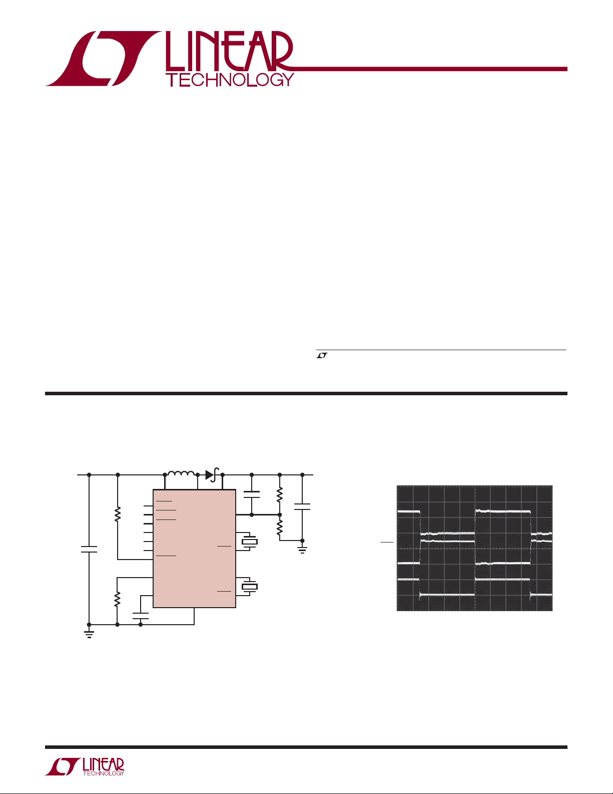
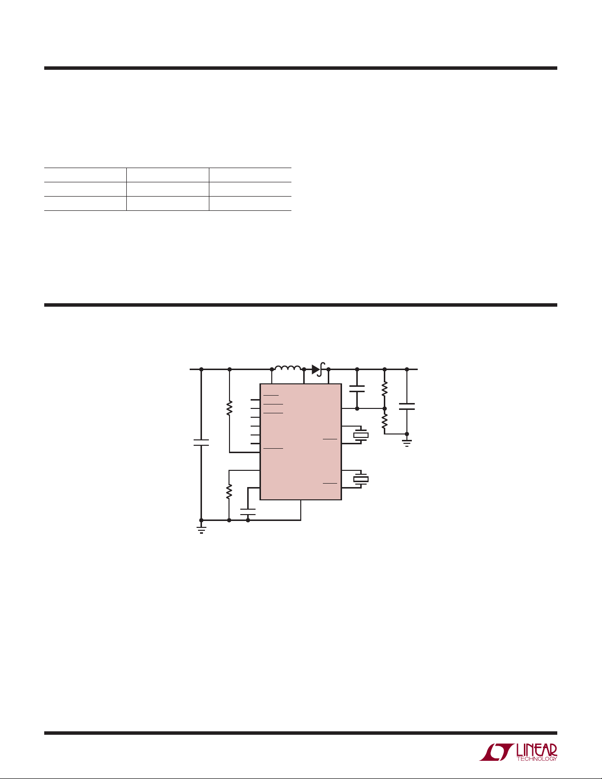
TYPICAL APPLICATION
DESCRIPTION
The LT®3572 is a highly integrated dual Piezo motor driver
capable of driving two Piezo motors at up to 40V from a
5V supply. Each Piezo driver can be independently turned
on or off along with the boost converter.
The boost regulator has a soft-start capability that limits the
inrush current at start-up. The boost regulator switching
frequency is set by an external resistor or the frequency can
be synchronized by an external clock. A PGOOD pin indicates
when the output of the boost converter is in regulation and
the Piezo drivers are allowed to start switching.
The LT3572 is available in a (4mm × 4mm) 20-pin QFN
package.
, LT, LTC and LTM are registered trademarks of Linear Technology Corporation.
All other trademarks are the property of their respective owners.
V
3V TO 5V
Dual Piezo Driver
SHDN
SHDNA
SHDNB
PWMA
PWMB
SYNC
PGOOD
RT
SS
10nF
10μH
15pF
V
SW
GND
V
OUT
OUTA
OUTA
OUTB
OUTB
FB
IN
LT3572
576k
24.3k
IN
100k
4.7μF
42.2k
V
30V
50mA
10μF
3572 TA01a
OUT
Response Driving Piezo Motor at 70kHz
V
OUTA
20V/DIV
V
OUTA
20V/DIV
PWMA
2V/DIV
2μs/DIV
3572 TA01b
3572fa
1
LT3572
ABSOLUTE MAXIMUM RATINGS
(Note 1)
V
Voltage .............................................................40V
OUT
OUTA, OUTA, OUTB, OUTB Voltage ...........................40V
SW Voltage ...............................................................42V
RT, SS, SYNC ..............................................................2V
FB ............................................................................... 3V
All Other Pins ............................................................10V
Maximum Junction Temperature........................... 125°C
Operating Temperature Range (Note 2).... –40°C to 85°C
Storage Temperature Range ...................–65°C to 125°C
ORDER INFORMATION
PIN CONFIGURATION
TOP VIEW
GND
OUTA
OUTA
OUTB
20 19 18 17 16
1
SW
V
2
IN
SYNC
3
RT
4
GND
5
20-LEAD (4mm s 4mm) PLASTIC QFN
T
EXPOSED PAD (PIN 21) IS GND, MUST BE SOLDERED TO PCB
JMAX
21
6 7 8
PWMB
= 125°C, θJA = 37°C/W
OUT
V
PWMA
UF PACKAGE
9 10
GND
OUTB
SHDN
PGOOD
15
SS
14
FB
13
SHDNB
12
SHDNA
11
LEAD FREE FINISH TAPE AND REEL PART MARKING PACKAGE DESCRIPTION TEMPERATURE RANGE
LT3572EUF#PBF LT3572EUF#TRPBF 3572 20-Lead (4mm × 4mm) Plastic DFN –40°C to 85°C
Consult LTC Marketing for parts specifi ed with wider operating temperature ranges.
Consult LTC Marketing for information on non-standard lead based fi nish parts.
For more information on lead free part marking, go to: http://www.linear.com/leadfree/
For more information on tape and reel specifi cations, go to: http://www.linear.com/tapeandreel/
ELECTRICAL CHARACTERISTICS
The ● denotes the specifi cations which apply over the full operating
temperature range, otherwise specifi cations are at TA = 25°C. VIN = 5V, V
SHDNA
= V
SHDNB
= V
5V, unless otherwise noted.
SHDN =
PARAMETER CONDITIONS MIN TYP MAX UNITS
Minimum Operating Voltage
Quiescent Current VFB = 1.3V 3.4 4 mA
V
IN
Shutdown Current V
V
IN
SHDN
= V
SHDNA
= V
= 0V 0 1 μA
SHDNB
●
2.5 2.7 V
SHDN Pin Threshold 0.3 1.5 V
SHDNA Pin Threshold 0.3 1.5 V
SHDNB Pin Threshold 0.3 1.5 V
SHDN Pin Bias Current V
SHDNA Pin Bias Current V
SHDNB Pin Bias Current V
V
V
V
SHDN
SHDN
SHDN
SHDN
SHDN
SHDN
= 5V, V
= 0V, V
= 0V, V
= 0V, V
= 0V, V
= 0V, V
SHDNA
SHDNA
SHDNA
SHDNA
SHDNA
SHDNA
= 0V, V
= 0V, V
= 5V, V
= 0V, V
= 0V, V
= 0V, V
SHDNB
SHDNB
SHDNB
SHDNB
SHDNB
SHDNB
= 0V
= 0V
= 0V
= 0V
= 5V
= 0V
8
0.1
8
0.1
8
0.1
15
15
15
1
μA
μA
μA
1
μA
μA
1
μA
2
3572fa
LT3572
ELECTRICAL CHARACTERISTICS
The ● denotes the specifi cations which apply over the full operating
temperature range, otherwise specifi cations are at T
PARAMETER CONDITIONS MIN TYP MAX UNITS
PWMA Pin Threshold 0.3 1.5 V
PWMB Pin Threshold 0.3 1.5 V
PGOOD Rising Threshold (Note 3)
PGOOD Falling Threshold (Note 4)
PGOOD Resistance
Switching Frequency RT = 75.0kΩ
Maximum Duty Cycle RT = 75.0kΩ
Synchronization Frequency 575 2500 kHz
SYNC Pin Thresholds (Note 5) 0.3 1.5 V
SS Current 4.5 μA
FB Pin Voltage
FB Pin Voltage Line Regulation V
FB Pin Bias Current V
SW Current Limit (Note 7) 0.9 1.3 1.7 A
SW V
CESAT
SW Leakage Current SW = 40V 0.2 5 μA
OUTx Rise Time C = 2.2nF, V
OUTx Fall Time C = 2.2nF, V
= 25°C. VIN = 5V, V
A
RT = 13.0kΩ
RT = 13.0kΩ
= 2.5V to 10V 0.01 0.05 %/V
IN
= 1.225V (Note 6) 50 200 nA
FB
ISW = 800mA 310 450 mV
= 30V (Note 8) 120 ns
OUT
= 30V (Note 8) 120 ns
OUT
SHDNA
= V
SHDNB
= V
5V, unless otherwise noted.
SHDN =
●
1.12 1.16 1.19 V
●
1.01 1.04 1.065 V
●
●
425
●
1.9
●
95
●
85
●
1.195 1.225 1.255 V
500
2.25
13 kΩ
575
2.6
kHz
MHz
%
%
Note 1: Stresses beyond those listed under Absolute Maximum Ratings
may cause permanent damage to the device. Exposure to any Absolute
Maximum Rating condition for extended periods may affect device
reliability and lifetime.
Note 2: The LT3572 is guaranteed to meet specifi ed performance from
0°C to 70°C operating junction temperature. Specifi cations over the
–40°C to 85°C operating junction temperature range are assured by
design, characterization and correlation with statistical process controls.
Note 3: Rising threshold voltage on FB pin that pulls PGOOD low.
Note 4: Falling threshold voltage on FB pin that causes a high impedance
on PGOOD.
Note 5: Minimum pulse width is 100ns. Maximum off pulse width is 100ns.
Note 6: Current fl ows into the pin.
Note 7: Current limit guaranteed by design and/or correlation to static test.
Note 8: OUTx refers to OUTA, OUTA, OUTB, OUTB.
3572fa
3
LT3572
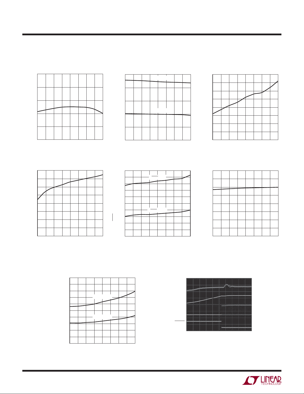
TYPICAL PERFORMANCE CHARACTERISTICS
Feedback Pin Voltage vs
Temperature
1.25
1.24
1.23
1.22
FEEDBACK VOLTAGE (V)
1.21
1.20
–50
–25 0
25 75 150
TEMPERATURE (°C)
50
100 125
3572 G01
Oscillator Frequency vs
Temperature
2.5
2.0
1.5
1.0
FREQUENCY (MHz)
0.5
0
–50
–25 0
25 75 150
TEMPERATURE (°C)
RT = 13k
RT = 35k
50
Quiescent Current vs Temperature SHDN Pin Current vs Temperature
4.0
3.5
3.0
2.5
2.0
1.5
1.0
QUIESCENT CURRENT (mA)
0.5
0
–25
–50
0
25
TEMPERATURE (°C)
50
75
100
125
150
3572 G04
10
9
8
7
6
5
4
3
SHDN PIN CURRENT (μA)
2
1
0
–50
–25 25
0
TEMPERATURE (°C)
V
V
SHDN
SHDN
= 5V
= 2.5V
50
75
100 125
125
100
3572 G02
3572 G05
150
SS Pin Current vs Temperature
8
7
6
5
4
3
SS PIN CURRENT (μA)
2
1
0
–25
–50
0
50
25
TEMPERATURE (°C)
75
SW Current Limit vs Temperature
1.6
1.4
1.2
1.0
0.8
0.6
PEAK CURRENT (A)
0.4
0.2
0
–25
–50
0
50
25
TEMPERATURE (°C)
75
100
100
125
125
150
3572 G03
150
3572 G06
4
SW Saturation Voltage vs
Temperature
0.50
0.45
0.40
0.35
0.30
0.25
0.20
0.15
0.10
SWITCH SATURATION VOLTAGE (V)
0.05
0
–50
–25 25
ISW = 800mA
ISW = 400mA
0
50
TEMPERATURE (°C)
Start-Up
I
IN
200mA/DIV
V
OUT
20V/DIV
V
OUTA
20V/DIV
PGOOD
5V/DIV
200μs/DIV
125
100
75
150
3572 G07
3572 G08
3572fa

PIN FUNCTIONS
LT3572
SW (Pin 1): Switch Node. This pin connects to the collector of an internal NPN power switch.
(Pin 2): Input Supply Pin. This pin must be locally
V
IN
bypassed with a capacitor.
SYNC (Pin 3): Synchronization Pin. This pin is used to
synchronize the internal oscillator to an external signal.
The synchronizing range is 15% above the free running
frequency set by the RT pin up to 2.5MHz. If not used,
this pin must be tied to GND.
RT (Pin 4): Frequency Set Pin. Place a resistor to GND
to set the internal frequency. The range of oscillation is
500kHz to 2.25MHz.
GND (Pins 5, 9, 20): Ground.
PWMB (Pin 6): Logic Input for the Driver. A high signal
on this input sets OUTB high and OUTB low.
PWMA (Pin 7): Logic Input for the Driver. A high signal
on this input sets OUTA high and OUTA low.
(Pin 8): Output for the Switching Regulator and the
V
OUT
Input Supply for the Drivers.
SHDN (Pin 10): Shutdown Pin. Tie to 1.5V or more to
enable the switcher. Pull low to disable the switcher.
SHDNA (Pin 11): Shutdown Pin. Tie to 1.5V or more to
enable OUTA and OUTA. Pull low to place OUTA and OUTA
in a high impedance state.
SHDNB (Pin 12): Shutdown Pin. Tie to 1.5V or more to
enable OUTB and OUTB. Pull low to place OUTB and OUTB
in a high impedance state.
FB (Pin 13): Feedback Pin. The LT3572 regulates this pin
to 1.225V. Connect the feedback resistors to this pin to
set the output voltage for the switching regulator.
SS (Pin 14): Soft-Start Pin. Place a soft-start capacitor
here. A capacitor on the soft-start pin slowly ramps the
current limit of the part from 0A to 1.3A.
PGOOD (Pin 15): This pin is an open-drain output that
pulls low when the FB pin is within 95% of its regulation
value.
OUTB (Pin 16): The Output Driver. This node switches
between V
OUTB (Pin 17): The Output Driver. This node switches
between V
OUTA (Pin 18): The Output Driver. This node switches
between V
OUTA (Pin 19): The Output Driver. This node switches
between V
Exposed Pad (Pin 21): Ground. The Exposed Pad of the
package provides both electrical contact to ground and
good thermal contact to the printed circuit board. The
Exposed Pad must be soldered to the circuit board for
proper operation.
and GND and is inverted from OUTB.
OUT
and GND.
OUT
and GND .
OUT
and GND and is inverted from OUTA.
OUT
3572fa
5

LT3572
BLOCK DIAGRAM
8
V
OUT
OUTA
18
Q2
Q3
7
PWMA
+
A2
A6
10
SHDN
START-UP/
INTERNAL BIAS
A4
S
Q
R
11
SHDNA12SHDNB
V
IN
2
L1
SW
1
Q1
–
OUTA
19
OUTB
17
OUTB
16
Q4
Q5
Q6
OSCILLATOR
Q7
Q8
Q9
A5
R
C
C
C
Q10
+
GND
A3
R5
–
1.225V
+
A1
–
95%/85%
–
A7
GND
GND
GND
5
9
20
21
FB
13
SS
14
+
D1
V
OUT
R1
R2
C2
R4
C1
PWMB4RT3SYNC
6
R3
PGOOD
15
3572 F01
Figure 1. Block Diagram
6
3572fa

OPERATION
LT3572
Switching Regulator
The LT3572 uses a constant frequency, current mode,
control scheme to provide excellent line and load regulation
for the output drivers. Operation can be best understood
by referring to the Block Diagram in Figure 1. A pulse
from the oscillator sets the RS fl ip-fl op, A4, and turns on
the internal NPN bipolar power switch, Q1. Current in Q1
and the external inductor, L1, begins to increase. When
this current exceeds a level determined by the voltage at
the output of the error amplifi er A1, comparator A2 resets
A4, turning Q1 off. The current in L1 fl ows through the
external Schottky diode D1 and begins to decrease. The
cycle begins again at the next pulse from the oscillator.
In this way, the voltage at the output of the error amplifi er
controls the current through the indictor to the output. The
soft-start capacitor, C2, clamps the output of the error
amplifi er causing the current limit to slowly increase. This
helps reduce overshoot on the output and helps minimize
inrush current on the input.
Output Drivers
The function of the driver section is to level shift the
input of the PWM pins to the voltage of the V
drivers operate in an H-bridge fashion, where the OUTA
and OUTB pins are the same polarity as the PWMA and
PWMB pins respectively and the OUTA and OUTB are
inverted from PWMA and PWMB respectively. The OUT
pins will be high impedance until the FB pin is within
95% of its regulated voltage. The OUT pins will follow
PWMA and PWMB as long as FB stays within 85% of the
regulated voltage. If FB drops below 85%, the OUT pins
will go high impedance.
pin. The
OUT
3572fa
7

LT3572
APPLICATIONS INFORMATION
Duty Cycle
The typical maximum duty cycle of the LT3572 is 95% at
1MHz. This maximum duty cycle reduces as the switching frequency is increased. The duty cycle for a given
application is given by:
VVV
++–
DC
OUT D IN
=
VVV
OUT D CESAT
–
where VD is the diode forward drop, typically 0.5V and
V
is, in the worst case, 310mV at 0.8A. The LT3572
CESAT
can be used at higher duty cycles, but must be operated
in the discontinuous mode so that the actual duty cycle
is reduced.
FB Resistor Network
The output voltage is programmed with a resistor divider
between the output and the FB pin. Choose the resistors
according to:
RR
12
⎛
⎜
⎝
1 225
.
OUT
⎞
1=
–
⎟
⎠
V
V
Shutdown Pins
When held below 0.3V, SHDNA and SHDNB prevent the
drivers from switching and keep the outputs in a high
impedance state. If SHDN is held below 0.3V then the
switching regulator is prevented from turning on. When
any one of these pins are pulled above 1.5V the internal
circuitry is turned on and the respective output is allowed
to operate. When the LT3572 is not in use all three pins
should be pulled low.
Oscillator
The LT3572 can operate at switching frequencies from
500kHz up to 2.25MHz by changing the value of the resistor R3 on the RT pin. Figure 2 shows a graph of RT vs
Switching Frequency.
The oscillator can be synchronized with an external clock
applied to the SYNC pin. When synchronizing the oscillator, the free running frequency must be set approximately
10000
1000
SWITCHING FREQUENCY (kHz)
100
10
Figure 2. RT Resistance vs Switching Frequency
RT RESISTANCE (kΩ)
100
3572 F02
15% lower than the desired synchronized frequency. If
the sync function is not used the SYNC pin must be tied
to ground.
PGOOD
The part has a power good feature that detects when the
output boost converter is up and in regulation. When the
part is turned off or not in regulation the PGOOD pin is
in a high impedance state. When the part is within 95%
of regulation the PGOOD pin is pulled low signaling that
the output is valid. If the output then falls below 85% of
regulation the PGOOD pin is put back in a high impedance
state. Whenever the output is not in regulation the output
pins in the driver aren’t allowed to switch and are placed
in a high impedance state. The PGOOD pin is an open
drain of an NMOS devices with an impedance of 1kΩ and
should be tied to V
through a resistor.
IN
Soft-Start
The soft-start feature limits the inrush current drawn from
the supply upon start-up. An internal current source with a
nominal 4.5μA current source charges an external capacitor
C2. The voltage on the soft-start pin is used to control the
output of the error amplifi er, which limits the maximum
peak current through the inductor and the inrush current
drawn from the supply during start-up.
8
3572fa

APPLICATIONS INFORMATION
LT3572
PWM
The LT3572 can PWM the output drivers at a very high
frequency. The limitation on the frequency is determined
by the internal rise in die temperature that occurs when
driving the motor. The power delivered to the piezo motor
2
is propotional to V
, the capacitance of the motor, and
OUT
the PWM frequency. When any of these are increased the
power dissipated in the part increases causing the internal
die temperature to increase. Driving two 2.2nF capacitors
with V
at 30V, the maximum PWM frequency should be
OUT
less than 80 kHz. The LT3572 can run at a higher frequency
but either V
needs to be reduced or the capacitance
OUT
needs to be lowered. A piezo motor has an associated
capacitance that cannot be reduced so the output voltage
2
must be lowered. Since the power is proportional to V
reduction of V
to 25V from 30V will allow the LT3572 to
OUT
OUT
a
run at a maxim frequency of 115 kHz. If a different motor is
used the maximum PWM frequency will need to be adjusted
inversely to the equivolent capacitance of the motor.
Inductor Selection
A 10μH inductor is recommended for most LT3572 applications. Choose an inductor that will handle at least
1A without saturating, and ensure that the inductor has a
2
low DCR (copper-wire resistance) to minimize I
R power
losses. Table 1 lists several inductor manufacturers.
Table 1. Inductor Manufacturers
Sumida (847) 956-0666 www.sumida.com
TDK (847) 803-6100 www.tdk.com
Murata (714) 852-2001 www.murata.com
FDK (408) 432-8331 www.tdk.co.jp
Capacitor Selection
The small size of ceramic capacitors makes them ideal
for LT3572 applications. Only X5R or X7R types should
be used because they retain their capacitance over wider
voltage and temperature ranges than other types such as
Y5V or Z5U. A 4.7μF to 15μF output capacitor is suffi cient
for stable transient response, however, more output capacitance can help limit the voltage droop on V
OUT
during
transients.
Ceramic capacitors also make a good choice for the input
decoupling capacitor, which should be placed as close as
possible to the LT3572. A 1μF to 4.7μF input capacitor
is suffi cient for most applications. Table 2 shows a list
OUTB
OUTA
C1
PWMB
OUTA
20
6
PWMA
19
GND
7
V
OUT
D1
L1
1
SW
V
2
C3
IN
3
SYNC
4
RT
GND
5
R4
OUTB
18
17
16
PGOOD
15
SS
14
13
FB
12
SHDNB
11
8
9
10
SHDN
SHDNA
C2
R2
R1
C
FF
3572 BD LAYOUT
3572fa
9
LT3572
APPLICATIONS INFORMATION
of several ceramic capacitor manufacturers. Consult the
manufacturers for detailed information on their entire
selection of ceramic parts.
Table 2. Ceramic Capacitor Manufacturers
Taiyo Yuden (408) 573-4150 www.t-yuden.com
AVX (803) 448-9411 www.avxcorp.com
Murata (714) 852-2001 www.murata.com
Diode Selection
A Schottky diode is recommended for use with the LT3572.
The Philips PMEG 3005 is a good choice. If the switch
voltage exceeds 30V, a PMEG 4005 (a 40V diode) can be
TYPICAL APPLICATION
L1
V
3V TO 5V
IN
R4
100k
C3
4.7μF
R3
34k
12μH
218
10
11
12
15
14
7
6
3
4
C2
10nF
V
SHDN
SHDNA
SHDNB
PWMA
PWMB
SYNC
PGOOD
RT
SS
SW
IN
LT3572
GND
used. These diodes are rated to handle an average forward
current of 0.5A. For higher effi ciency, use a diode with better thermal characteristics such as the On Semiconductor
MBRM140 (a 40V diode).
Layout Hints
As with all switching regulators, careful attention must be
paid to the PCB board layout and component placement.
To maximize effi ciency, switch rise and fall times are made
as short as possible. Note the vias under the Exposed Pad.
These should connect to a local ground plane for better
thermal performance.
D1
V
OUT
OUTA
OUTA
OUTB
OUTB
5, 9, 20, 21
C4
R1
20pF
576k
13
FB
18
19
17
16
R2
24.9k
V
30V
50mA
C1
10μF
3572 TA02
OUT
10
3572fa

PACKAGE DESCRIPTION
4.50 p 0.05
3.10 p 0.05
2.00 REF
RECOMMENDED SOLDER PAD PITCH AND DIMENSIONS
APPLY SOLDER MASK TO AREAS THAT ARE NOT SOLDERED
4.00 p 0.10
2.45 p 0.05
2.45 p 0.05
4.00 p 0.10
PIN 1
TOP MARK
(NOTE 6)
UF Package
20-Lead Plastic QFN (4mm × 4mm)
(Reference LTC DWG # 05-08-1710 Rev A)
0.70 p0.05
PACKAGE OUTLINE
0.25 p0.05
0.50 BSC
0.75 p 0.05
R = 0.05
TYP
2.00 REF
BOTTOM VIEW—EXPOSED PAD
R = 0.115
TYP
2.45 p 0.10
2019
LT3572
PIN 1 NOTCH
R = 0.20 TYP
OR 0.35 s 45o
CHAMFER
0.40 p 0.10
1
2
0.200 REF
0.00 – 0.05
NOTE:
1. DRAWING IS PROPOSED TO BE MADE A JEDEC PACKAGE OUTLINE MO-220
VARIATION (WGGD-1)—TO BE APPROVED
2. DRAWING NOT TO SCALE
3. ALL DIMENSIONS ARE IN MILLIMETERS
4. DIMENSIONS OF EXPOSED PAD ON BOTTOM OF PACKAGE DO NOT INCLUDE
MOLD FLASH. MOLD FLASH, IF PRESENT, SHALL NOT EXCEED 0.15mm ON ANY SIDE
5. EXPOSED PAD SHALL BE SOLDER PLATED
6. SHADED AREA IS ONLY A REFERENCE FOR PIN 1 LOCATION
ON THE TOP AND BOTTOM OF PACKAGE
2.45 p 0.10
(UF20) QFN 01-07 REV A
0.25 p 0.05
0.50 BSC
Information furnished by Linear Technology Corporation is believed to be accurate and reliable.
However, no responsibility is assumed for its use. Linear Technology Corporation makes no representation that the interconnection of its circuits as described herein will not infringe on existing patent rights.
3572fa
11
LT3572
RELATED PARTS
PART NUMBER DESCRIPTION COMMENTS
LT1160 Half-/Full-Bridge N-Channel MOSFET Driver V
LT3469 Piezo Microactuator Driver with Boost Regulator V
LT3479 3A, Full Featured DC/DC Converter with Soft-Start and Inrush
Current Protection
LT3580 42V, 2A, 2.5MHz High Effi ciency Step-Up DC/DC Converter VIN: 2.5V to 32V, V
: 10V to 15V, V
IN
: 2.5V to 16V, V
IN
Piezo Microactuator
: 2.5V to 24V, V
V
IN
DFN, TSSOP Packages
3mm × 3mm DFN8 and MS8E Packages
= 60V, 24-Lead SO Package
OUT(MAX)
= 35V Maximum, 40mA Current Limit for
OUT
= 40V, IQ = Analog/PWM, ISD < 1μA,
OUT(MAX)
= 40V, IQ = 1mA, ISD < 1μA,
OUT(MAX)
12
Linear Technology Corporation
1630 McCarthy Blvd., Milpitas, CA 95035-7417
(408) 432-1900 ● FAX: (408) 434-0507 ● www.linear.com
3572fa
LT 0408 REV A • PRINTED IN USA
© LINEAR TECHNOLOGY CORPORATION 2007
 Loading...