

DESIGN FEATURES L
I
APD
= 1mA 500ns/DIV
500µV/DIV
C1
1µF
MONIN
V
REF
R
T
SHDN
CTRL
GND
SYNC
V
OUT
FB
V
IN
SW
LT3571
MON APD
OFF ON
V
IN
5V
R2
20.5k
R4
49.9Ω
45V
R
T
12.1k
1MHz
R
SENSE
20Ω
C4
0.1µF
C3
10nF
R3
10k
C5
10nF
L: TDK VLF3010AT – 100MR49
C1: TDK X7R C1608X7R1C105KT
C2, C4: MURATA X7R GRM188R72A104KA35
C3: AVX X7R 06031C103K
C5: MURATA X7R GRM155R71H103K
50V
C2
0.1µF
L1
10µH
R1
1M
Complete APD Bias Solution in 60mm2
with On-the-Fly Adjustable Current
Limit and Adjustable V
Introduction
The overriding factor limiting functionality in fiber-optic communication
systems is available space. A compact
APD (avalanche photo diode) bias
solution with a high degree of feature
integration is the key to breaking
new ground in system size and performance. The LT3571 offers such a
solution in a tiny 3mm × 3mm QFN
package.
The LT3571 combines a current
mode step-up DC/DC converter and
a high side fixed voltage drop APD
current monitor with an integrated
75V power switch and Schottky diode.
The combination of a traditional voltage loop and a unique current loop
allows customers to set an accurate
APD current limit at any given bias
voltage. The integrated high side current monitor provides an 8% accurate
current that is proportional to the load
current, making it possible to adjust
the APD bias voltage via the CTRL
pin. This feature-rich device makes
it possible to produce a single stage
boost converter to bias high voltage
APDs in only 60mm2.
Low Noise APD Bias Supply
The gain of the APD is dependent on the
bias voltage, so the bias supply must
minimize the noise contamination
from switching regulators and other
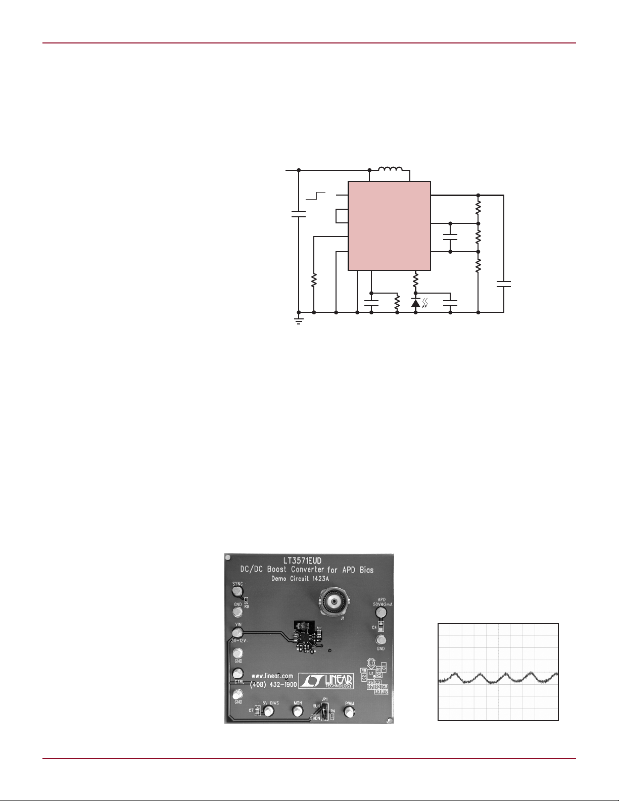
sources. Figure 1 shows the LT3571
configured to produce an ultralow
noise power supply for a 45V APD
with 2.5mA of load current capability.
The MONIN voltage is regulated by
the internal voltage reference and the
resistor divider made up of R1 and R2.
Resistor R
APD current limit at 200mV/1.2R
– 0.2mA.
internal reference, making it possible
The CTRL pin can override the
to optimize the APD bias on the fly
to maximize receiver performance.
SENSE
is selected to set the
SENSE
When the CTRL pin is connected to a
supply above 1V, the output voltage is
regulated with feedback at 1V. When
driven below 1V, the feedback and the
output voltage follow accordingly.
The APD pin, the output of the current monitor, provides a voltage to the
APD load that is fixed 5V below the
MONIN pin. The LT3571 includes a
precise current mirror with a factor of-five attenuation. The proportional
current output signal at the MON pin
can be used to accurately indicate the
Figure 2. The LT3571 evaluation board
APD
Figure 1. Low noise APD bias supply
By Xin (Shin) Qi
APD signal strength. The voltage variance of APD pin voltage is only ±200mV
over the entire input current range and
the whole temperature range. Figure
2 shows the evaluation board for this
topology.
The topology uses several filter
capacitors to achieve ultralow noise
performance. The capacitor at V
pin and the 0.1µF capacitor at the
APD pin suppress switching noise. The
10nF feedforward capacitor across the
MONIN and FB pins filters out high
frequency internal reference and error
amplifier noise. Figure 3 shows the
measured switching noise is less than
500µV
at 1mA load current. This
P–P
exceptionally low noise bias voltage
Figure 3. AC-coupled noise ripple at APD pin
OUT
Linear Technology Magazine • March 2009
27
L DESIGN FEATURES
C1
1µF
MONIN
V
REF
R
T
SHDN
CTRL
GND
SYNC
V
OUT
FB
V
IN
SW
LT3571
MON APD
OFF ON
V
IN
5V
R2
15k
R4
49.9Ω
50V
R
T
33.2k
400kHz
R
SENSE
49.9Ω
C4
0.1µF
C3
10nF
R3
10k
C5
10nF
Q1
L1: TDK VLF4012AT – 150MR63
C1: TDK X7R C1608X7R1C105KT
C2: MURATA X7R GRM21AR72A224KAC5L
C3: AVX X7R 06031C103K
C4: MURATA X7R GRM188R72A104KA35
C5: MURATA X7R GRM155R71H103K
C6: MURATA X7R GRM155R71A104KA01D
55V
C2
0.22µF
L1
15µH
R1
1M
R7
49.9k
R5
30.1k
R6
100k
R9
20kC60.1µF
R8
36.5k
Q2
TEMPERATURE
COMPENSATION BLOCK
Q1, Q2 = PHILIPS PEMT1
50ns/DIV
PWM GND
PWM
1V/DIV
OUT
500mV/DIV
TRD< 100ns
I
APD
= 1mA
I
APD
= 10µA
OUT GND
50ns/DIV
PWM GND
PWM
1V/DIV
OUT
500mV/DIV
TFD< 100ns
I
APD
= 10µA
I
APD
= 1mA
OUT GND
C1
1µF
MONIN
V
REF
R
T
SHDN
CTRL
GND
SYNC
V
OUT
FB
V
IN
SW
LT3571
MON APD
OFF ON
V
IN
3.3V
R2
18.2k
50V
R
T
26.1k
500kHz
L1: TDK VLF3010AT-100MR49
C1: MURATA X7R GRM21BR71C105KA01B
C2, C3: MURATA X7R GRM188R72A104KA35
R
SENSE
20Ω
55V
2.5V
C2
0.1µF
C3
0.1µF
L1
10µH
R1
1M
+
–
PMBT3904
0.5pF
4.99k
4.99k
0.1µF
LT1815
APD PIN
PWM
1k
–V
LO
–V
HI
MEASURE
HERE
FOR TEST PURPOSES,
REPLACE APD WITH
THIS SIMPLE TEST SETUP
gives the APD greater sensitivity and
dynamic range.
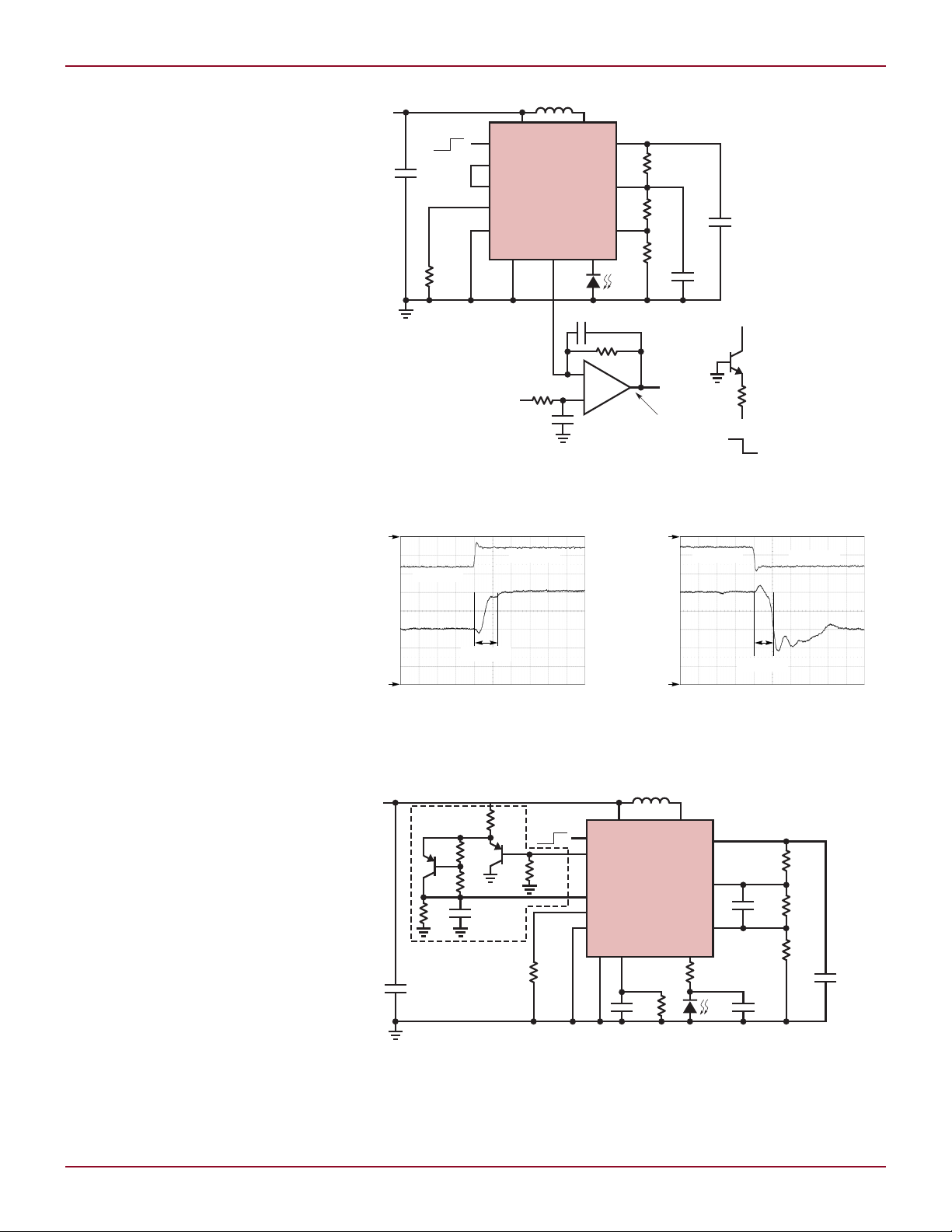
Fast APD Current Monitor
Transient Response
Design efforts in modern communications systems increasingly focus
on 10Gbits/s GPON systems, which
demand that the transient response of
the APD current monitor is less than
100ns for a two-decades-of-magnitude
input current step. To meet this challenging requirement, many designers
rely on a simple discrete current mirror
topology to reduce parasitic capacitance on the signal path, sacrificing
monitor accuracy and board space. In
contrast, the LT3571’s APD current
monitor is carefully designed to provide
not only a fixed voltage drop and high
accuracy, but also the required fast
transient response.
Figure 4 shows a compact circuit
that responds quickly to current
transients. Unlike the ultralow noise
topology shown in Figure 1, the filter
capacitor at the APD pin is moved to
the MONIN pin. C2, C3 and R
a π filter to isolate the APD current
monitor from high frequency switching
noise. The capacitor at the MON pin is
also removed to reduce the transient
delay on the measurement path.
The transient speed is measured
using the same technique described in
the Linear Technology Design Note 447
“A Complete Compact APD Bias Solution for a 10GBit/s GPON System.”
Figures 5 and 6 show the measured
input signal falling transient response
and input signal rising transient response, respectively, where the input
current levels are 10µA and 1mA.
Note that there is an inversion and
DC offset present in the measurement.
The measurements show a transient
response time of less than 100ns, well
within the stringent speed demands of
the 10Gbits/s GPON system.
APD Bias Voltage
Temperature Compensation
Typically, the APD reverse bias voltage
is designed with a compensatory positive temperature coefficient. This can
be easily implemented via the CTRL
pin of the LT3571—a less complex
28
form
SENSE
Figure 4. APD bias supply with ultrafast current monitor transient speed
Figure 5. Transient response on input
signal falling edge (1mA to 10µA)
Figure 7. Temperature-compensated APD power supply
Figure 6. Transient response on input
signal rising edge (10µA to 1mA)
Linear Technology Magazine • March 2009

DESIGN FEATURES L
V V V
BE Q BE Q BE( ) ( )1 2
= =
dV
dT
dV
dT
mV
C
BE Q BE Q( ) ( )1 2
2
= =
°
V V
R
R
V
CTRL REF BE
= −
8
7
PTC
dV
dT
RRmV
C
CTRL
= = •
872
°
R
R
V
V
mV
CVdV dT
REF
BE
OUT
OUT
8
7
2
=
+ •
°
R
R
V
dV
dT
mV
C
V
mV
C
V
BE
OUT
OUT
REF
1
2
2
2
1=
• + •
•
°
°
−
dV
dT
dV
dT
mV
C
BE Q BE Q( ) ( )1 2
2
= =
°
TEMPERATURE (°C)
–50
V
APD
(V)
60
42
58
54
50
46
56
52
48
44
40
7525 125500 100–25
OUTPUT CURRENT (A)
0.1
EFFICIENCY (%)
100
90
80
70
60
50
40
0.5 0.90.3 0.7 1.1 1.3
VIN = 15V
VIN = 8V
VIN = 30V
Authors can be contacted
at (408) 432-1900
and expensive solution than typical
microprocessor-controlled methods.
The simplest scheme uses a resistor
divider from the V
pin to the CTRL
REF
pin, where the top resistor in the divider is an NTC (negative temperature
coefficient) resistor. While simple,
this method suffers from nonlinear
temperature coefficient of the NTC
resistor. A more precise method uses
a transistor network as shown in Figure 7. The PTC (Positive Temperature
Coefficient) of the CTRL pin voltage is
Figure 8. Temperature response
of the circuit shown in Figure 7
realized by an emitter follower of Q1
and a VBE multiplier of Q2.
Assuming:
and
then the CTRL pin voltage is
with
Given V
at room and dV
OUT
OUT
/DT,
the R1/R2 and R8/R7 can be calculated as follows
Resistors R5–R9 are selected to make
I(Q1) = I(Q2) ≈ 10µA, and
Simulation using LTspice always
gives a good starting point. The circuit
shown in Figure 7 is designed to have
V
= 50V (V
APD
dV
/dT = 100mV/°C (dV
APD
= 55V) at room and
OUT
OUT
/dT =
100mV/°C). The measured temperature response is shown in Figure 8,
which is very close to the design
target.
Conclusion
The LT3571 is a highly integrated,
compact solution to APD bias supply
design. It provides a useful feature set
and the flexibility to meet a variety of
challenging requirements, such as low
noise, fast transient response speed,
and temperature compensation. With
a high level of integration and superior performance, the LT3571 is the
natural choice for APD bias supply
design.
L
LT8410, continued from page 23
out of shutdown, the V
discharged for 70µs with a strong pull
down current, and then charged with
10µA to 1.235V. This achieves soft
start since the output is proportional
to V
. Full soft-start cycles occur
REF
even with short SHDN low pulses
since V
part is enabled.
In addition, the LT8410/-1 features
a 2.5V to 16V input voltage range, up
LT3653/63, continued from page 21
of handling 60V transients. Figure 4
shows the circuit efficiency at multiple
input voltages.
The current limit of the application
is set to 1.2A, therefore, the power path
components are sized to handle 1.2A
maximum. To reduce the application
footprint, the LT3663 includes internal
compensation and a boost diode. The
RUN pin, when low, puts the LT3663
into a low current shutdown mode.
Linear Technology Magazine • March 2009
pin is first
REF
is discharged when the
REF
to 40V output voltage and overvoltage
protection for CAP and V
OUT
.
Conclusion
The LT8410/-1 is a smart choice
for applications which require low
quiescent current and low input current. The ultralow quiescent current,
combined with high value integrated
feedback resistors, keeps the average
input current very low, significantly
Figure 4. Efficiency of the circuit in Figure 3
extending battery operating time.
Low current limit internal switches
(8mA for the LT8410-1, 25mA for the
LT8410) make the part ideal for high
impedance sources such as coin cell
batteries. The LT8410/-1 is packed
with features without compromising
performance or ease of use and is
available in a tiny 8-pin 2mm × 2mm
package.
L
Conclusion
The accurate programmable output
current limit of the LT3653 and
LT3663 eliminates localized heating
from an output overload, reduces the
maximum current requirements on the
power components, and makes for a
robust power supply solutions.
L
29
 Loading...