

L DESIGN FEATURES
V
IN1
SHDN1
SHDN2
SHDN3
SHDN1
SHDN2
SHDN3
SW1
FB1
100nF
1nF
100nF
10µF
1µF
2.5V
40mA
31.6k
3.3V
1A
22k
143k
12V
275mA
5V
22k
10.2k
10.2k
21.5k
10.2k
22.1k
10µF
10µF
1nF
100nF
3.3µH
4.7µH
D2
D3
D1
BOOST
SW2
FB2
SS2
NPN_DRV
FB3
V
C2
SS1
V
C1
V
IN2VIN3
BIAS
RTSYNC
LT3570
GND
Q1
)
/54
!
%&&)#)%.#9
6).66
/54
6
6
/54
6)
/54
M!
6
/54
6)
/54
M!
Buck, Boost and LDO Regulators
Combined in a 4mm × 4mm QFN
Introduction
The LT3570 simp lifies compl ex
multi-rail power supply designs by
integrating three DC/DC regulators
into a single package: a current mode
buck regulator, a current mode boost
regulator, and an LDO controller.
The buck and boost regulators
each have a current limit of 1.5A. The
LDO controller has an output current
capability of 10mA and combines with
an external NPN transistor to create
a linear regulator. The frequency of
the switching regulators can be set
from 500kHz to 3MHz by an external
resistor or synchronized to an external oscillator. The independent input
voltages for each regulator offers a
wide operating range from 2.5V up to
40V. Each regulator also has its own
shutdown circuitry and the buck and
boost regulators have their own softstart circuitry.
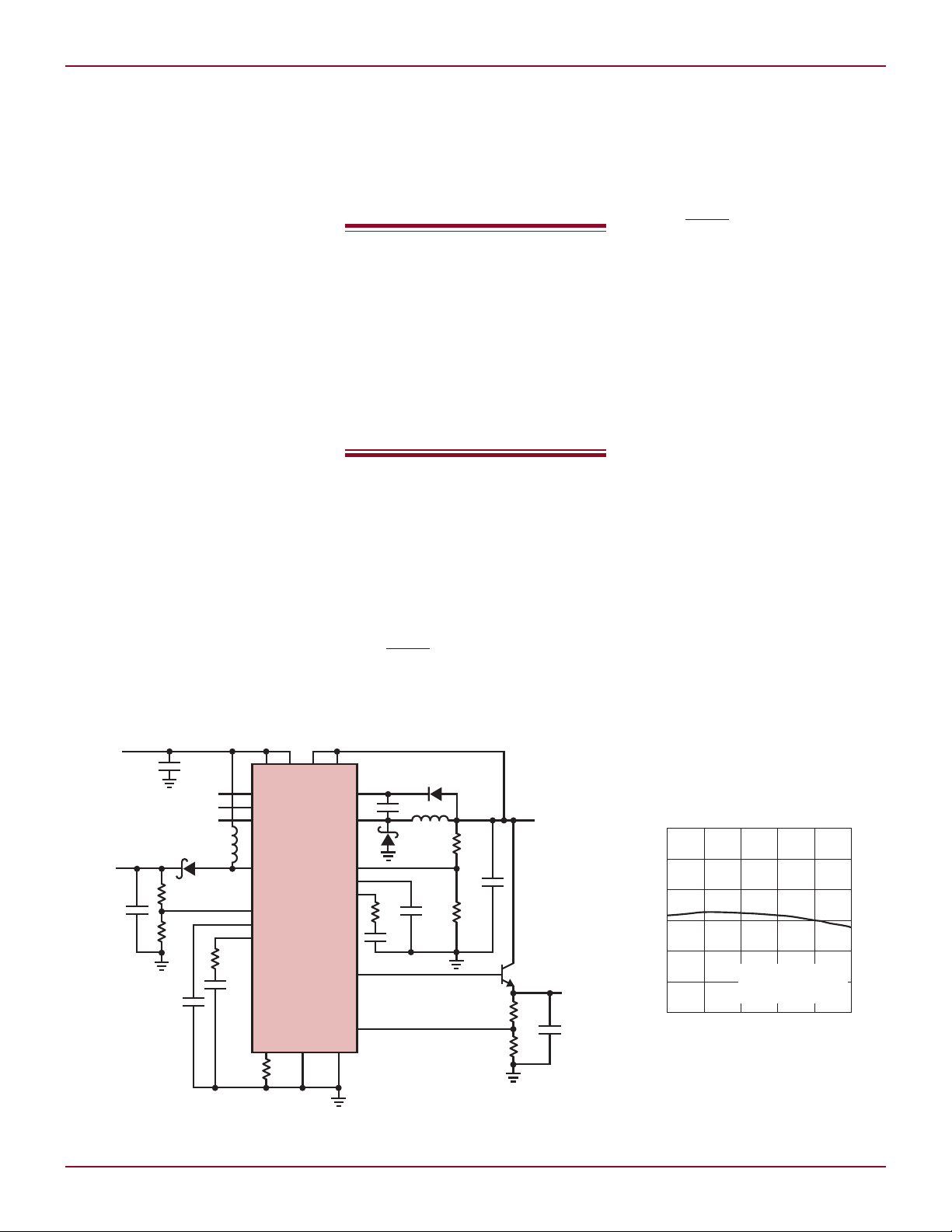
The typical application shown in
Figure 1 generates 3.3V at 1A from
the buck regulator, 2.5V at 40mA from
the LDO controller and 12V at 275mA
from the boost regulator, all from a
5V input supply voltage and with an
overall efficiency around 85%.
Features
Available in either a 24-lead 4mm
× 4mm QFN or a 20-pin TSSOP
package, the LT3570 is a constant
frequency current mode regulator.
If all SHDN pins are held low, zero
quiescent current is drawn from the
input supplies and the part is turned
The LT3570 simplifies
complex multi-rail
power supply designs by
integrating three DC/DC
regulators into a single
package: a current mode
buck regulator, a current
mode boost regulator, and
an LDO controller.
by Chris Falvey
off. Any SHDN pin voltage exceeding
1.5V will turn on the corresponding
regulator. A precise shutdown pin
threshold allows for easy integration
of input supply undervoltage lockout.
All three regulators share the same
internal 800mV reference voltage. For
each regulator, an external resistor
divider programs the output voltage
to any value above the part’s reference
voltage. The switching frequency is
set with an external resistor from the
RT pin to GND. This allows a trade off
between minimizing component size
(by using higher switching frequencies) and maximizing efficiency (by
using lower switching frequencies).
Additionally, running at a low switching frequency allows for applications
that require larger VIN-to-V
The adjustable and synchronizable
switching frequency also allows the
user to keep the switching noise out of
critical wireless and audio bands.
Both the buck and boost regulators
control the slew rate of the output
ratios.
OUT
28
Figure 1. A typical 5V input to 3.3V, 2.5V and 12V application
Linear Technology Magazine • June 2008

V
IN1
SHDN1
SHDN2
SHDN3
SHDN1
SHDN2
SHDN3
SW1
FB1
C8
100nF
C7
1nF
C5
10nF
C2
10µF
C3
1µF
V
OUT3
3.3V
500mA
R3
340k
V
OUT2
5V
R8
25k
R1
100k
V
OUT1
8V
250mA
V
IN
8V TO 30V
R7
25k
R2
11k
R4
64.9k
R5
205k
R6
64.9k
R9
24.9k
C9
10µF
C1
10µF
C6
1nF
10nF
L2
10µH
10µH
D2
D3
D1
BOOST
SW2
FB2
SS2
NPN_DRV
FB3
V
C2
SS1
V
C1
V
IN2VIN3
BIAS
RTSYNC
LT3570
GND
Q1
300µs PROPAGATION DELAY
– 2mV DC STEP
I
OUT1
200mA/
DIV
V
OUT1
100mV/
DIV
V
OUT2
100mV/
DIV
100µs/DIV
300µs PROPAGATION DELAY
– 2mV DC STEP
V
OUT1
20V/
DIV
V
IN
5V/
DIV
V
OUT2
5V/
DIV
1ms/DIV
Figure 2. Dying gasp system keeps power even when battery is disconnected.
V
IN1
SHDN1
SHDN2
SHDN3
SW1
FB1
C8
100nF
C7
1nF
C5
10nF
10µF
C3
1µF
V
OUT3
2.5V
100mA
R3
205k
V
OUT2
3.3V
200mA
R8
25k
R1
1.10M
V
OUT1
36V
V
IN
12V
R7
25k
R2
23.7k
R4
64.9k
R5
137k
R6
64.9k
R9
24.9k
C9
10µF
C1
10µF
C6
1nF
C4
10nF
L2
10µH
L1
10µH
D2
D3
D1
BOOST
SW2
FB2
SS2
NPN_DRV
FB3
V
C2
SS1
V
C1
V
IN2VIN3
BIAS
RTSYNC
LT3570
GND
Q1
voltage during start-up. A controlled
ramp reduces inrush current on the
input supply and minimizes output
overshoot. An external capacitor connected between the SS pin and ground
programs the slew rate. The voltage
on the SS pin overrides the internal
reference voltage to the error amplifier
and is charged by a 4.5µA internal
current source.
DESIGN FEATURES L
The BIAS pin allows the internal
circuitry to draw current from a lower
voltage supply than the input, reducing power dissipation and increasing
efficiency. Normally, the quiescent
current is supplied from V
the voltage on the BIAS pin exceeds
2.5V the current is supplied from the
BIAS pin. The BIAS pin is only available
on the 24-lead QFN package.
, but when
IN2
Figure 3. Output waveforms when power
is removed from the circuit in Figure 2
Applications
“Dying Gasp” Application
The LT3570 provides an ideal solution for any “dying gasp” system.
Figure 2 shows a typical application
powering an airbag controller. In an
automobile accident, the battery may
get disconnected from the shock sensors yet the airbag must still fire. In
this application, the battery supplies
power to the boost regulator. V
set to 36V and drives V
and V
IN2
the inputs to the buck regulator and
the LDO controller, respectively. Even
after the input supply is removed, the
buck regulator and the LDO continue
to function properly for more than
3ms, as the energy continues to be
supplied from the output capacitor of
the boost regulator. The buck regulator
turns off when V
approaches the
IN2
input undervoltage lockout of 2.3V
(see Figure 3).
continued on page 41
OUT1
is
IN3,
Figure 4. DSL modem application
Linear Technology Magazine • June 2008
Figure 5. Step response of Figure 4 with boost
current stepped from 200mA to 400mA
29

POWER LOSS (mW)
EFFICIENCY (%)
LOAD CURRENT (A)
100.1
100
0
10k
100
1
1k
10
20
30
40
50
60
70
80
90
VIN = 24V
V
OUT3
= 12V
2+1 MODE
EFFICIENCY
POWER LOSS
CONTINUOUS MODE
PULSE-SKIPPING MODE
BURST MODE OPERATION
V
OUT1,2
200mV/DIV
I
L2
2A/DIV
I
L1
2A/DIV
25µs/DIV
VIN = 14V
V
OUT1,2
(NOM) = 1.8V
LOAD STEP ON V
OUT1,2
= 1A TO 6A
Figure 2. Post-package trimming of the
LTC3853’s current sense comparators
provides excellent current sharing between
channels 1 and 2, even during a transient.
sync with frequencies between 250kHz
and 750kHz.
The LTC3853 can be set to operate
in one of three modes under light load
conditions. Burst Mode operation offers the highest light load efficiency by
switching in a “burst” of one to several
pulses replenishing the charge stored
in the output capacitors, followed by a
long sleep period when the load current
is supplied by the output capacitors.
Forced continuous mode offers fixed
frequency operation from no load to
full load, providing the lowest output
voltage ripple at the cost of light load
efficiency. Pulse-skipping mode operates by preventing inductor current
reversal by turning off the synchronous switch as needed. This mode
is a compromise between the other
two modes, offering lower ripple than
Burst Mode operation and better light
load efficiency than forced continuous
mode. Regardless of the mode selected,
the LTC3853 operates in constant frequency mode at higher load currents.
Figure 3 shows the efficiency in each
of the three modes.
Each of the LTC3853’s channels
can be enabled with its own RUN
pin, or slewed up or down with its
own TRACK/SS pin. Tracking holds
the feedback voltage to the lesser of
the internal reference voltage or the
voltage on TRACK/SS, which can be
brought up with an external ramp or
with its own 1.2µA internal current
source. With all of the TRACK/SS
pins held low and any output enabled
through its RUN pin, the 5V INTVCC is
still available for ancillary keep-alive
circuits.
Pulse-skipping mode is always
enabled at start-up to prevent sinking current from a pre-biased output
voltage. When the output reaches 80%
of the set value, the part switches over
to forced continuous mode until the
output has entered the POWER GOOD
window, at which point it switches
over to the selected mode of operation. Forced continuous mode reduces
the output ripple as the power good
threshold is crossed, to ensure that
the POWER GOOD indicators make
just one low to high transition.
Three different max current comparator sense thresholds can be set
via the ILIM pin. The current is sensed
using a high speed rail-to-rail differential current sense comparator. The
circuit of Figure 1 uses accurate sense
resistors between the inductors and
the outputs. For reduced power loss at
high load currents, the LTC3853 can
also monitor the parasitic resistance
of the inductor (DCR sensing). Peak
inductor current is limited on a cycleby-cycle basis and is independent
of duty cycle. If load current is high
enough to cause the feedback voltage
DESIGN IDEAS L
Figure 3. Efficiency for channel 3 in Figure 1—
in each of the three modes of operation
to drop, current limit fold back protects
the power components by reducing the
current limit. For predictable tracking,
current limit fold back is disabled
during start-up. Input undervoltage
lockout, output overvoltage shutdown
and thermal shutdown also protect
the power components and the IC
from damage.
Conclusion
The LTC3853’s small footprint belies
its versatility and extensive feature
set. From inputs up to 24V it can
regulate three separate outputs, or it
can be configured for higher currents
by tying channels 1 and 2 together.
Either way, the phase relationship
between channels is automatically
optimized to reduce ripple currents.
At low duty cycles, the short minimum
on-time ensures constant frequency
operation, and peak current limit
remains constant even as duty cycle
changes. The cost-effective LTC3853
incorporates these features, and
more, into a 40-pin 6mm × 6mm QFN
package.
L
LT3570, continued from page 29
DSL Modem
Figure 4 shows an application for a
DSL modem or set-top box. The supply voltage for V
adapter that can range from 8V to 30V.
IN2
comes from a wall
This voltage is stepped down to 5V at
100mA for V
the power to drive both the boost
regulator and LDO controller. V
is set to 8V at 200mA and V
Linear Technology Magazine • June 2008
, which then supplies
OUT2
OUT3
is set
OUT1
to 3.3V at 500mA. Figure 5 shows the
load step response of V
with a 200mA load step on V
OUT1
and V
OUT1
Conclusion
The LT3570 is a monolithic dual
output switching regulator (buck and
boost) with a NPN LDO controller and
is ideal for a broad variety of applications. Because the LT3570 offers a high
OUT2
.
level of system integration, it greatly
simplifies board design for complex
applications that need multiple voltage supply rails. With the flexibility of
independent supply inputs and adjustable frequency, the user can set a wide
array of custom output voltages. The
LT3570 is a feature rich solution that
satisfies the needs for multiple output
voltages in a compact solution.
L
4141
 Loading...