

Application Note 5
December 1984
Thermal Techniques in Measurement and Control Circuitry
Jim Williams
Designers spend much time combating thermal effects in
circuitry. The close relationship between temperature and
electronic devices is the source of more design headaches
than any other consideration.
In fact, instead of eliminating or compensating for thermal
parasitics in circuits, it is possible to utilize them. In particular, applying thermal techniques to measurement and
control circuits allows novel solutions to diffi cult problems.
The most obvious example is temperature control. Familiarity with thermal considerations in temperature control
loops permits less obvious, but very useful, thermallybased circuits to be built.
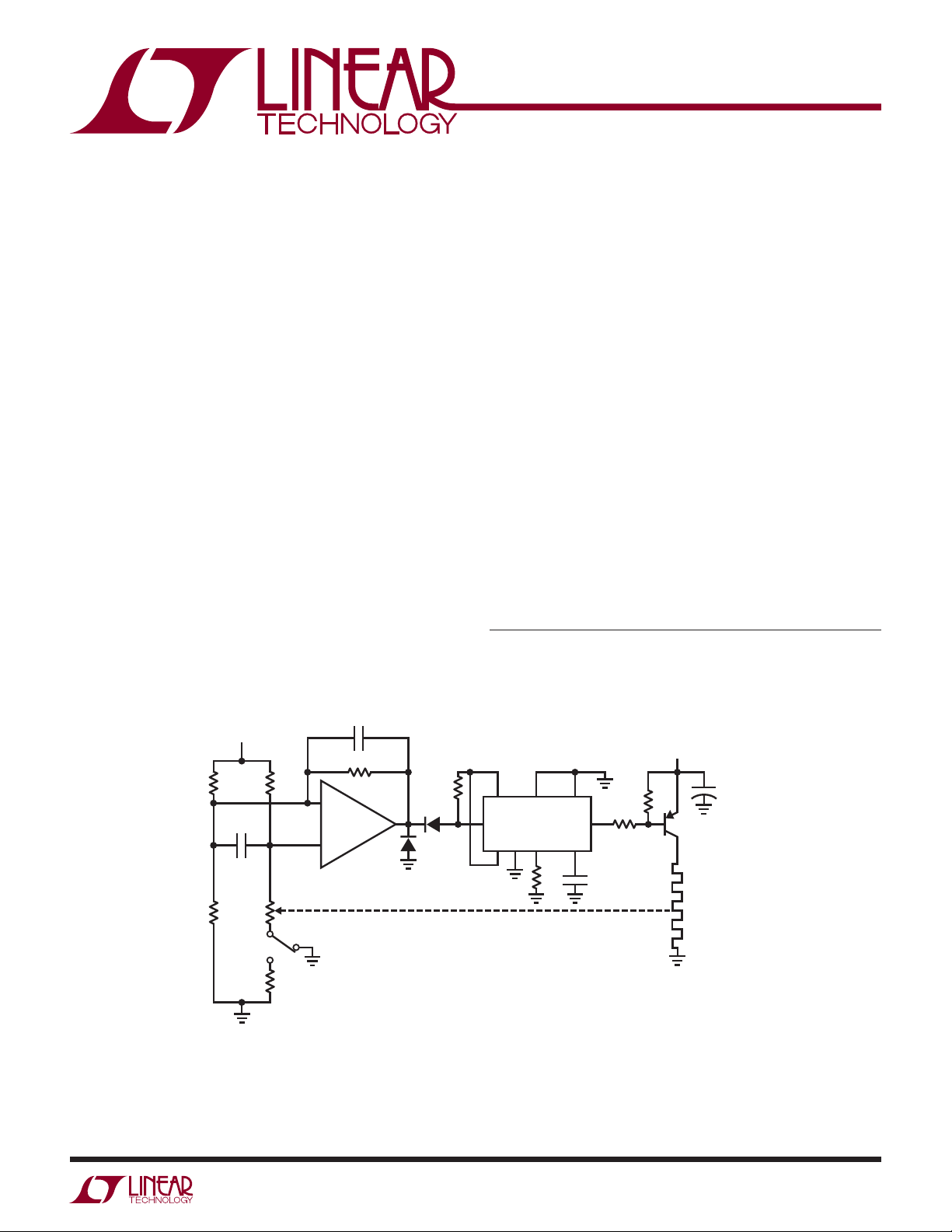
Temperature Controller
Figure 1 shows a precision temperature controller for
a small components oven. When power is applied, the
thermistor, a negative TC device, is at a high value. A1
®
saturates positive. This forces the LT
15V
100k*
100k*
0.05
100k*
R
T
3525A switching
0.02
100M
–
+
A1
LT1012
1N914
1N914
10k
THERMAL FEEDBACK
regulator’s output low, biasing Q1. As the heater warms,
the thermistor ’s value decreases. When its inputs fi nally
balance, A1 comes out of saturation and the LT3525A pulse
width modulates the heater via Q1, completing a feedback
path. A1 provides gain and the LT3523A furnishes high
effi ciency. The 2kHz pulse width modulated heater power
is much faster than the thermal loop’s response and the
oven sees an even, continuous heat fl ow.
The key to high performance control is matching the gain
bandwidth of A1 to the thermal feedback path. Theoretically, it is a simple matter to do this using conventional
servo-feedback techniques. Practically, the long time
constants and uncertain delays inherent in thermal systems
present a challenge. The unfortunate relationship between
servo systems and oscillators is very apparent in thermal
control systems.
L, LT, LTC, LTM, Linear Technology and the Linear logo are registered trademarks of Linear
Technology Corporation. All other trademarks are the property of their respective owners.
15V
141116
LT3525A
12 6 5
5k
139
0.015
≈2kHz
1k
2k
+
47
Q1
2N5023
20Ω HEATER
50Ω
STEP TEST
50Ω ≈ 0.01°C
*TRW MAR-6 RESISTOR
= YSI #44014 RT = 300k AT 25°C
R
T
Figure 1. Precision Temperature Controller
AN05 F01
an5f
AN5-1
Application Note 5
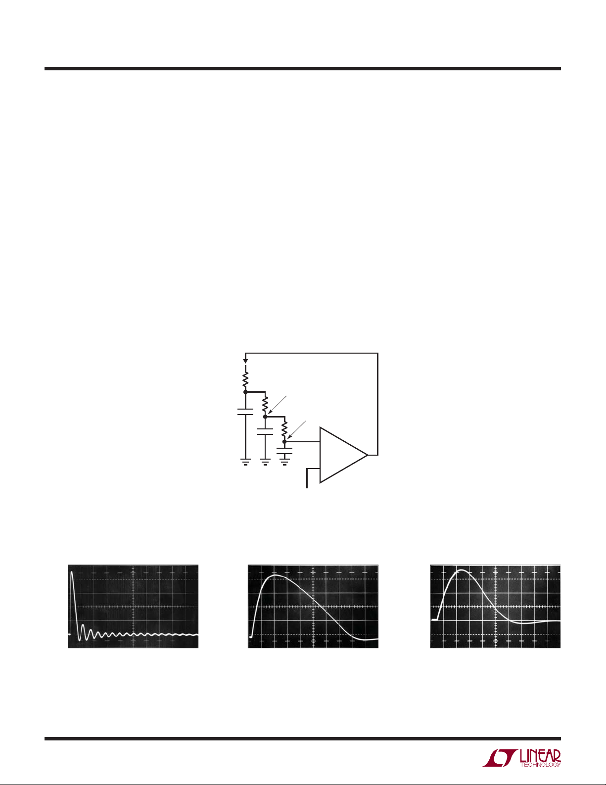
The thermal control loop can be very simply modeled as
a network of resistors and capacitors. The resistors are
equivalent to the thermal resistance and the capacitors
equivalent to thermal capacity. In Figure 2 the heater,
heater-sensor interface, and sensor all have RC factors
that contribute to a lumped delay in the ability of a thermal system to respond. To prevent oscillation, A1’s gain
bandwidth must be limited to account for this delay. Since
high gain bandwidth is desirable for good control, the
delays must be minimized. The physical size and electrical resistivity of the heater selected give some element of
control over the heater’s time constant. The heater-sensor
interface time constant can be minimized by placing the
sensor in intimate contact with the heater.
The sensor ’s RC product can be minimized by selecting a
sensor of small size relative to the capacity of its thermal
environment. Clearly, if the wall of an oven is 6" thick
aluminum, the tiniest sensor available is not an absolute
necessity. Conversely, if one is controlling the temperature
of 1/16" thick glass microscope slide, a very small sensor
(i.e., fast) is in order.
After the thermal time constants relating to the heater and
sensor have been minimized, some form of insulation for
the system must be chosen. The function of insulation
is to keep the loss rate down so the temperature control
device can keep up with the losses. For any given system, the higher the ratio between the heater-sensor time
constants and the insulation time constants, the better
the performance of the control loop.
After these thermal considerations have been attended
to, the control loop’s gain bandwidth can be optimized.
Figures 3A, 3B and 3C show the effects of different compensation values at A1. Compensation is trimmed by applying small steps in temperature setpoint and observing
the loop response at A1’s output. The 50Ω resistor and
2V/DIV
HEATER
OR CURRENT CORRESPONDING TO TEMPERATURE)
Figure 2. Thermal Control Loop Model
0.5V/DIV
5 SECONDS/DIV
ABC
AN05 F03a
HEATER-SENSOR INTERFACE
SENSOR
TEMPERATURE REFERENCE
(CAN BE A RESISTANCE, VOLTAGE
2 SECONDS/DIV
AN05 F02
AN05 F03b
0.5V/DIV
HORIZONTAL = 0.5 SECONDS/DIV
AN05 F03c
AN5-2
Figure 3. Loop Response for Various Gain Bandwidths
an5f

Application Note 5
switch in the thermistor leg of the bridge furnish a 0.01°C
step generator. Figure 3A shows the effects of too much
gain bandwidth. The step change forces a damped, ringing
response over 50 seconds in duration! The loop is marginally stable. Increasing A1’s gain bandwidth (GBW) will force
oscillation. Figure 3B shows what happens when GBW is
reduced. Settling is much quicker and more controlled. The
waveform is overdamped, indicating that higher GBW is
achievable without stability compromises. Figure 3C shows
the response for the compensation values given and is a
nearly ideal critically damped recovery. Settling occurs
within 4 seconds. An oven optimized in this fashion will
easily attenuate external temperature shifts by a factor of
thousands without overshoots or excessive lags.
Thermally Stabilized PIN Photodiode Signal
Conditioner
PIN photodiodes are frequently employed in wide range
photometric measurements. The photodiode specifi ed in
Figure 4 responds linearly to light intensity over a 100dB
range. Digitizing the diode’s linearly amplifi ed output
would require an A/D converter with 17 bits of range.
This requirement can be eliminated by logarithmically
compressing the diode’s output in the signal conditioning circuity. Logarithmic amplifi ers utilize the logarithmic
relationship between V
and collector current in transis-
BE
tors. This characteristic is very temperature sensitive and
requires special components and layout considerations
to achieve good results. Figure 4’s circuit logarithmically
signal conditions the photodiode’s output with no special
components or layout.
A1 and Q4 convert the diode’s photocurrent to a voltage
output with a logarithmic transfer function. A2 provides
offsetting and additional gain. A3 and its associated components form a temperature control loop which maintains
Q4 at constant temperature (all transistors in this circuit
are part of a CA3096 monolithic array). The 0.033μF value
at A3’s compensation pins gives good loop damping if the
circuit is built using the array’s transistors in the locations
shown. These locations have been selected for optimal
control at Q4, the logging transistor. Because of the array
15V
LT1021-10V
OUT
IN
Q4
500pF
50k*
1M
750k*
1M
FULL-SCALE
TRIM
0.01
46
10
5
11
Q5
2k
12
50k
DARK
TRIM
–
A1
10k*
LT1012
+
10k*
2k
15
14
Q1 Q3
13
–
A3
LM301A
+
0.033
3k
33Ω
7
8
9
15V
I
P
–
A2
LM107
+
1
2
3
Q2
AN05 F04
= HP-5082-4204 PIN PHOTODIODE
Q1 TO Q5 = CA3096
CONNECT SUBSTRATE OF CA3096
ARRAY TO Q4’s EMITTER
*1% RESISTOR
E
OUT
LIGHT
(900 NANOMETERS)
1mW
100μW
10μW
1μW
100nW
10nW
RESPONSE DATA
DIODE CURRENT
350μA
35μA
3.5μA
350nA
35nA
3.5nA
CIRCUIT OUTPUT
10.0V
7.85V
5.70V
3.55V
1.40V
–0.75V
Figure 4. 100dB Range Logarithmic Photodiode Amplifi er
an5f
AN5-3

Application Note 5
die’s small size, response is quick and clean. A full-scale
step requires only 250ms to settle (photo, Figure 5) to fi nal
value. To use this circuit, fi rst set the thermal control loop.
To do this, ground Q3’s base and set the 2k pot so A3’s
negative input voltage is 55mV below its positive input. This
places the servo’s setpoint at about 50°C (25°C ambient
+ 2.2mV/°C • 25°C rise = 55mV = 50°C). Unground Q3’s
base and the array will come to temperature. Next, place
the photodiode in a completely dark environment and
adjust the “dark trim” so A2’s output is 0V. Finally, apply
or electrically simulate (see chart, Figure 4) 1mW of light
and set the “full-scale” trim to 10V out. Once adjusted,
this circuit responds logarithmically to light inputs from
10nW to 1mW with an accuracy limited by the diode’s
1% error.
0.2V/DIV
50MHz Bandwidth Thermal RMS→DC Converter
Conversion of AC waveforms to their equivalent DC power
value is usually accomplished by either rectifying and
averaging or using analog computing methods. Rectifi cation averaging works only for sinusoidal inputs. Analog
computing methods are limited to use below 500kHz.
Above this frequency, accuracy degrades beyond the
point of usefulness in instrumentation applications. Additionally, crest factors greater than 10 cause signifi cant
reading errors.
A way to achieve wide bandwidth and high crest factor
performance is to measure the true power value of the
waveform directly. The circuit of Figure 6 does this by
measuring the DC heating power of the input waveform.
15V
90k*
90k*
10k
0.01
INPUT
*0.1% RESISTOR
T1, T2 = YELLOW SPRINGS INST. CO.
THERMISTOR COMPOSITE
#44018
1μF = MYLAR
T1A
REDBRN
T1
T1B
10k
T2
T2B
GRNGRN
Figure 6. 50MHz Thermal RMS→DC Converter
HORIZONTAL = 50ms/DIV
AN05 F05
Figure 5. Figure 4’s Thermal Loop Response
100k*
BRNRED
T2A
1μF
300Ω*
1μF
–
+
–
+
0.01
A1
LT1002
100k*
0.01
A2
LT1002
10k* 10k*
–
10k*
15k
+
10k*
–
+
A3
LT1001
20k
FULL-SCALE
TRIM
A4
LT1001
1N4148
OUT
0V TO 10V
AN05 F06
an5f
AN5-4

Application Note 5
By using thermal techniques to integrate the input waveform, 50MHz bandwidth is easily achieved with 2% accuracy. Additionally, because the thermal integrator’s output
is at low frequency, no wideband circuitry is required.
The circuit uses standard components and requires no
special trimming techniques. It is based on measuring
the amount of power required to maintain two similar but
thermally decoupled masses at the same temperature.
The input is applied to T1, a dual thermistor bead. The
power dissipated in one leg (T1A) of this bead forces the
other section (T1B) to shift down in value, unbalancing
the bridge formed by the other bead and the 90k resistors.
This imbalance is amplifi ed by the A1-A2-A3 combination. A3’s output is applied to a second thermistor bead,
T2. T2A heats, causing T2B to decay in value. As T2B’s
resistance drops, the bridge balances. A3’s output adjusts
drive to T2A until T1B and T2B have equal values. Under
these conditions, the voltage at T2A is equal to the RMS
value of the circuit’s input. In fact, slight mass imbalances between T1 and T2 contribute a gain error, which
is corrected at A4. RC fi lters at A1 and A2 and the 0.01μF
capacitor eliminate possible high frequency error due to
capacitive coupling between T1A and T1B. The diode in
A3’s output line prevents circuit latch-up.
Figure 7 details the recommended thermal arrangement
for the thermistors. The Styrofoam block provides an
isothermal environment and coiling the thermistor leads
attenuates heat pipe effects to the outside ambient. The
2-inch distance between the devices allows them to see
identical thermal conditions without interaction. To calibrate this circuit, apply 10V
to the input and adjust the
DC
full-scale trim for 10V out at A4. Accuracy remains within
2% from DC to 50MHz for inputs of 300mV to 10V. Crest
factors of 100:1 contribute less than 0.1% additional error
and response time to rated accuracy is fi ve seconds.
Low Flow Rate Thermal Flowmeter
Measuring low fl ow rates in fl uids presents diffi culties.
“Paddle wheel” and hinged vane type transducers have low
and inaccurate outputs at low fl ow rates. If small diameter
tubing is required, as in medical or biochemical work,
such transduction techniques also become mechanically
impractical. Figure 8 shows a thermally-based fl owmeter
which features high accuracy at rates as low as 1mL/minute
and has a frequency output which is a linear function of
fl ow rate. This design measures the differential temperature
between two sensors (Figure 9). One sensor, T1, located
before the heater resistor, assumes the fl uid’s temperature
before it is heated by the resistor. The second sensor, T2,
picks up the temperature rise induced into the fl uid by the
resistor’s heating. The sensor ’s difference signal appears
at A1’s output. A2 amplifi es this difference with a time
constant set by the 10MΩ adjustment. Figure 10 shows
A2’s output versus fl ow rate. The function has an inverse
relationship. A3 and A4 linearize this relationship, while simultaneously providing a frequency output (Figure 10). A3
functions as an integrator which is biased from the LT1004
and the 383k input resistor. Its output is compared to A2’s
output at A4. Large inputs from A2 force the integrator to
run for a long time before A4 can go high, turning on Q1
and resetting A3. For small inputs from A2, A3 does not
have to integrate very long before resetting action occurs.
Thus, the confi guration oscillates at a frequency which is
inversely proportional to A2’s output voltage. Since this
voltage is inversely related to fl ow rate, the oscillation
frequency linearly corresponds to fl ow rate.
Several thermal considerations are important in this circuit.
The amount of power dissipated into the stream should be
constant to maintain calibration. Ideally, the best way to
do this is to measure the VI product at the heater resistor
and construct a control loop to maintain constant wattage
4"
BOTTOMTOP
2"
THERMISTORS
Figure 7. Thermal Arrangement for RMS→DC Converter
AN05 F07
2"
Styrofoam
0.5"
BLOCKS
AN5-5
an5f

Application Note 5
1M*
–15V
3.2k**
3.2k**
15V
15Ω
R
HEATER
100k
0.1
2.7k
383k*
LT1004-1.2V
*1% FILM RESISTOR
**SUPPLIED WITH YSI THERMISTOR NETWORK
YSI THERMISTOR NETWORK = #44201
R
HEATER
= DALE HL-25
–
LT1012
+
A3
6.25k**6.25k**
T2T1
Q1
2N4391
1M*
1M*
100k
–
+
1M*
1N4148
A1
LT1002
+
–
300pF
A4
LT1011
1
–15V
4
Figure 8. Liquid Flowmeter
100k
10M
RESPONSE
TIME
4.7k
100k
15V
OUTPUT
0Hz TO 300Hz =
0 TO 300mL/MIN
1μF
–
LT1002
+
A2
6.98k*
5k
FLOW
CALIBRATION
1k*
AN05 F08
IN
MIXING GRID
PREVENTS
LAMINER FLOW
FLOW
SENSOR T1
HEATER RESISTOR
15V
STAINLESS TUBING
OUT
SENSOR T2
SIZE TUBING O.D.
TO FIT RESISTOR I.D.
USE THERMAL COMPOUND
FOR GOOD HEAT TRANSFIER
AN05 F09
Figure 9. Flowmeter Transducer Details
dissipation. However, if the resistor specifi ed is used, its
drift with temperature is small enough to assume constant
dissipation with a fi xed voltage drive. Additionally, the fl uid’s
specifi c heat will affect calibration. The curves shown are
for distilled water. To calibrate this circuit, set a fl ow rate
of 10mL/minute and adjust the fl ow calibration trim for
10Hz output. The response time adjustment is convenient
for fi ltering fl ow aberrations due to mechanical limitations
in the pump driving the system.
280
240
200
T1-T2 (A2 OUTPUT)
VS FLOW CURVE
160
120
0.05V
80
40
FLOW FOR DISTILLED WATER (mL/MINUTE)
0
0
40 80
FREQUENCY VS FLOW CURVE
0.1V
0.22V
160
120 200
FREQUENCY (Hz)
0.66V0.44V
240 280
AN05 F10
Figure 10. Flowmeter Response Data
Thermally-Based Anemometer (Air Flowmeter)
Figure 11 shows another thermally-based fl owmeter, but
this design is used to measure air or gas fl ow. It works
by measuring the energy required to maintain a heated
resistance wire at constant temperature. The positive
temperature coeffi cient of a small lamp, in combination
with its ready availability, makes it a good sensor. A type
AN5-6
an5f

Application Note 5
2k 15V
Q1
27Ω
500k*
1W
AIR FLOW
RECOMMENDED
LAMP
ORIENTATION
Q1 = 2N6533
Q2 TO Q5 = CA3046 ARRAY [TIE PIN 13 (SUBSTRATE) TO –15V]
*1% RESISTOR
100k
100k*
–
LT1002
+
150k*
A1
0.1μF
500pF
1N4148
2k
33k
1k
ZERO
FLOW
Figure 11. Thermal Anemometer
328 lamp is modifi ed for this circuit by removing its glass
envelope. The lamp is placed in a bridge which is monitored
by A1. A1’s output is current amplifi ed by Q1 and fed back
to drive the bridge. The capacitors and 220Ω resistor
ensure stability. The 2k resistor furnishes start-up. When
power is applied, the lamp is at a low resistance and Q1’s
emitter tries to come full on. As current fl ows through the
lamp, its temperature quickly rises, forcing its resistance
to increase. This action increases A1’s negative input potential. Q1’s emitter voltage decreases and the circuit fi nds
a stable operating point. To keep the bridge balanced, A1
acts to force the lamp’s resistance, hence its temperature,
constant. The 10k-2k bridge values have been chosen so
that the lamp operates just below the incandescence point.
This high temperature minimizes the effects of ambient
temperature shifts on circuit operation. Under these conditions, the only physical parameter which can signifi cantly
infl uence the lamp’s temperature is a change in dissipation
characteristic. Air fl ow moving by the lamp provides this
change. Moving air by the lamp tends to cool it and A1
increases Q1’s output to maintain the lamp’s temperature.
The voltage at Q1’s emitter is nonlinearly, but predictably,
related to air fl ow by the lamp. A2, A3 and the array transistors form a circuit which squares and amplifi es Q1’s
emitter voltage to give a linear, calibrated output versus
air fl ow rate. To use this circuit, place the lamp in the air
fl ow so that its fi lament is a 90° angle to the fl ow. Next,
either shut off the air fl ow or shield the lamp from it and
adjust the zero fl ow potentiometer for a circuit output of
0V. Then, expose the lamp to air fl ow of 1000 feet/minute
and trim the full fl ow potentiometer for 10V output. Repeat
1N4148
Q2 Q3 Q5
1000pF
2k
–
A2
LT1002
+
150k*
500k
1μF
12k
3.3k
–15V
2M
FULL-SCALE
FLOW
–
LT1004-1.2V
+
A3
LM107
OUTPUT
0V TO 10V =
AN05 F11
0 TO 1000FT/MIN
these adjustments until both points are fi xed. With this
procedure completed, the air fl owmeter is accurate within
3% over the entire 0 to 1000 foot/minute range.
Low Distortion, Thermally Stabilized Wien Bridge
Oscillator
The positive temperature coeffi cient of lamp fi laments is
employed in a modern adaptation of a classic circuit in
Figure 12. In any oscillator it is necessary to control the
gain as well as the phase shift at the frequency of interest.
If gain is too low, oscillation will not occur. Conversely,
too much gain will cause saturation limiting. Figure 12
uses a variable Wien Bridge to provide frequency tuning
from 20Hz to 20kHz. Gain control comes from the positive
temperature coeffi cient of the lamp. When power is applied, the lamp is at a low resistance value, gain is high and
oscillation amplitude builds. As amplitude builds, the lamp
current increases, heating occurs and its resistance goes
up. This causes a reduction in amplifi er gain and the circuit
fi nds a stable operating point. The lamp’s gain-regulating
behavior is fl at within 0.25dB over the 20Hz-20kHz range
of the circuit. The smooth, limiting nature of the lamp’s
operation, in combination with its simplicity, gives good
results. Trace A, Figure 13 shows circuit output at 10kHz.
Harmonic distortion is shown in Trace B and is below
0.003%. The trace shows that most of the distortion is
due to second harmonic content and some crossover
disturbance is noticeable. The low resistance values in the
Wein network and the 3.8nV√Hz noise specifi cation of the
LT1037 eliminate amplifi er noise as an error term.
an5f
Information furnished by Linear Technology Corporation is believed to be accurate and reliable.
However, no responsibility is assumed for its use. Linear Technology Corporation makes no representation that the interconnection of its circuits as described herein will not infringe on existing patent rights.
AN5-7

Application Note 5
At low frequencies, the thermal time constant of the small
normal mode lamp begins to introduce distortion levels
above 0.01%. This is due to “hunting” as the oscillator’s
frequency approaches the lamp thermal time constant.
This effect can be eliminated, at the expense of reduced
output amplitude and longer amplitude settling time, by
switching to the low frequency, low distortion mode. The
four large lamps give a longer thermal time constant and
distortion is reduced. Figure 14 plots distortion versus
frequency for the circuit.
References
1. Multiplier Application Guide, pp. 7-9, “Flowmeter,”
Analog Devices, Inc., Norwood, Massachusetts.
LOW FREQ (<50Hz)
LOW DISTORTION MODE
NORMAL
MODE
L2-L5 #1891
L1 #327
100Ω
430Ω
2. Olson, J.V., “A High Stability Temperature Controlled
Oven,” S.B. Thesis M.I.T., Cambridge, Massachusetts,
1974.
3. PIN Photodiodes—5082-4200 Series, pp. 332-335,
Optoelectronics Designers’ Catalog, 1981, Hewlett
Packard Company, Palo Alto, California.
4. Y.S.I. Thermilinear Thermistor, #44018 Data Sheet,
Yellow Springs Instrument Company, Yellow Springs,
Ohio.
5. Hewlett, William R., “A New Type Resistance-Capacitor
Oscillator,” M.S. Thesis, Stanford University, Palo Alto,
California, 1939.
*1% FILM RESISTOR
10k DUAL POTENTIOMETER-
MATCH TRACKING 0.1%
MATCH ALL LIKE CAPACITOR
VALUES 0.1%
–
A = 10V/DIV
B = 0.01V/DIV
(0.003% DISTORTION)
20Hz-200Hz
0.82
953*
10k
HORIZONTAL = 20μs/DIV
200Hzm2kHz 2kHzm20kHz
0.082
0.0082
Figure 12. Low Distortion Sinewave Oscillator
AN05 F13
LT1037 OUTPUT
+
0.82
953*
10k
0.050
0.045
0.040
0.035
0.030
0.025
0.020
0.015
PERCENT DISTORTION
0.010
0.005
0
0
0.082 0.0082
NORMAL MODE
LOW FREQUENCY
LOW DISTORTION
MODE
20
FREQUENCY (Hz)
AN05 F12
200
2k
20k
AN05 F14
AN5-8
Linear Technology Corporation
1630 McCarthy Blvd., Milpitas, CA 95035-7417
(408) 432-1900 ● FAX: (408) 434-0507
●
www.linear.com
Figure 14. Oscillator Distortion vs FrequencyFigure 13. Oscillator Waveforms
an5f
IM/GP 0885 10K • PRINTED IN USA
© LINEAR TECHNOLOGY CORPORATION 1984
 Loading...