

L DESIGN IDEAS
V
C1
7.5k 4.7k
2.7nF 4.7nF
10µF
V
LDO
3.3V
0.5A
V
LOGIC
5V
0.5A
V
OFF
–10V
20mA
V
IN
8V TO 30V
22µF
L3
4.7µH
0.22µF
47nF 15nF 15nF 15nF
V
ON
22V
20mA
2.2µF
V
C3
30k
165k
232k
10k
1.5nF
VC2V
C1
GND
13k
2.2nF
V
C4
V
IN
V
LOGIC
5V
LDOPWR
LT3513
UVLO SW2
2.2µF
FB5 FB3
BD
FB1
SENSE
–
SENSE
+
SW1
BOOST
BIAS
SW3
L4
6.8µH
42.2k
DFLS240L
ZXTAM322
Si2333DS
DFLS240L
ZHCS400
10k
30.1k
10k
69.8k
L2
10µH
0.47µF
10k
60.4k
178k 53.6k 100k
10k
10µF
L1
10µH
AV
DD
8V
80mA
10µF
0.47µF
NFB4
D4
SW4
RUN-SS3/4
C
T
RUN-SS2
RUN-SS1
V
ONSINK
E3
V
ON
V
ON_CLKVON_CLK
PGOOD
FB2
V
LOGIC
5V
L1: SUMIDA CDR6D28MNNP-100NC L2: COILCRAFT LPO3310-103MLC
L3: SUMIDA CDR6D28MNNP-4R5NC L4: COILCRAFT LPO3310-682MLC
AVDD10V/DIV
RUN/SS 2V/DIV
V
LOGIC
5V/DIV
I
IN(AVG)
1A/DIV
V
OFF
10V/DIV
VE320V/DIV
VON20V/DIV
5ms/DIV
5-Output High Current Power
Supply for TFT-LCDs in a Low Profile
QFN Features Space-Saving 2MHz
Switching Regulators
Introduction
The LT3513 is a highly integrated,
5-output regulator designed to provide all the supply voltages typically
required by large TFT liquid crystal
displays (LCDs) with a single IC. The
part features a step-down switching
regulator to produce a 3.3V or 5V
logic voltage from a wide voltage range
input, such as automotive battery.
A lower voltage logic supply can be
generated from the first supply by
adding an external NPN driven by an
internal linear regulator. The other
three on-chip regulators provide the
three bias voltages required by LCDs: a
high power boost regulator to generate
AVDD, a low power boost regulator to
generate VON and an inverting regulator to provide V
Switching regulators are chosen
over linear regulators to accommodate
a wide input voltage range (providing
both step up and step down functions)
and to minimize power dissipation.
The LT3513’s wide input range, 4.5V
to 30V, allows it to accept a variety of
power sources, including automotive
batteries, distributed supplies and
wall transformers. The low profile
38-pin QFN package has an exposed
metal pad on the backside to maximize
thermal performance.
5-Output High Current Power Supply
for TFT-LCDs in a Low Profile QFN
Features Space-Saving 2MHz
Switching Regulators ........................30
Kevin Huang
32VIN Synchronous Buck Regulators
with Integrated FETs Deliver up to 12A
from Sub-1mm Height Packages ........32
Stephanie Dai and Theo Phillips
Complete Power Solution for Digital
Cameras and Other Complex Compact
Portable Applications ........................34
Brian Shaffer
30
30
.
OFF
by Kevin Huang
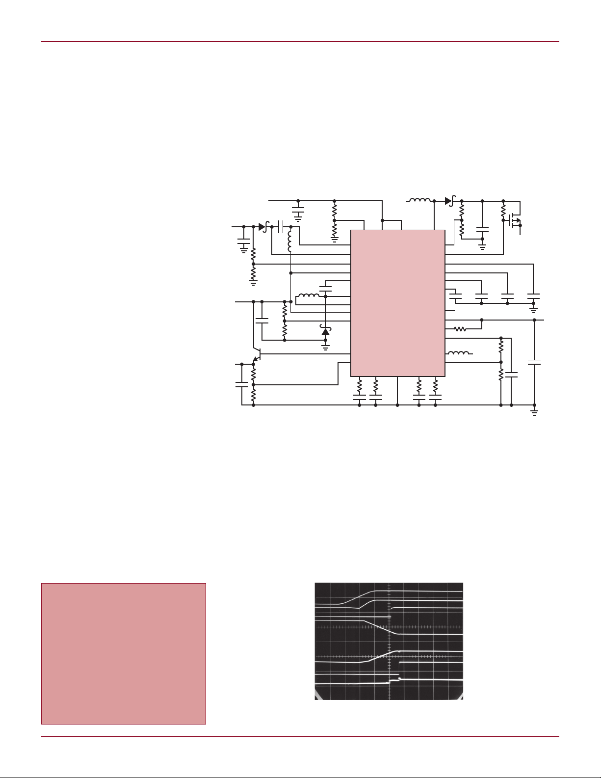
Figure 1. A complete 5-output 2MHz TFT-LCD power supply
Operation
All of the regulators are synchronized to a 2MHz internal clock,
allowing the use of small, low cost
inductors and ceramic capacitors.
Since different types of panels may require different bias voltages, all output
voltages are adjustable for maximum
flexibility. Programmable soft-start
capability is included in each of the
regulators to limit inrush current.
Figure 2. Startup waveforms of the power supply in Figure 1
Figure 1 shows a 5-output TFT LCD
power supply that can accommodate
an 8V to 30V input voltage. The first
switching converter produces a 5V
logic supply using a buck regulator.
The internal linear regulator with an
external NPN produces a 3.3V logic
supply using the 5V supply as input.
The second switcher is used to boost
the 5V supply to an 8V, 80mA AVDD
Linear Technology Magazine • September 2008

DESIGN IDEAS L
bias supply. Another boost converter
and an inverter generate VON and
V
, which also use the 5V supply
OFF
as input.
When power is first applied to the
input, the RUN-SS1 capacitor starts
charging. When its voltage reaches
0.8V, Switcher 1 is enabled. The capacitor at the RUN-SS1 pin controls
the ramp rate for the Switcher 1 output, V
and inrush current in L1.
LOGIC
Switchers 2, 3 and 4 are controlled
by the BIAS pin, which is usually
connected to V
. When the BIAS
LOGIC
pin is higher than 2.8V, the capacitors
at the RUNSS-2 and RUN-SS3/4 pin
begin charging to enable Switchers 2,
3 and 4. When AV
reaches 90% of
DD
its programmed voltage, the PGOOD
pin is pulled low. When AV
DD
, V
OFF
and
E3 all reach 90% or their programmed
voltages, the C
timer is enabled and a
T
20µA current source begins to charge
CT. When the C
pin reaches 1.1V, the
T
output PNP turns on, connecting E3
to VON. Figure 2 shows the start up
sequence of the circuit in Figure 1.
If one of the regulated voltages,
V
LOGIC
, AV
DD
, V
or E3 dips more
OFF
than 10%, the internal PNP turns off
to shut down VON. This action protects
the panels, as V
must be present to
ON
turn on the TFT display. The PGOOD
pin can drive an optional PMOS device
at the output of the boost regulator to
disconnect the load at AV
from the
DD
input during shutdown. The converter
uses all ceramic capacitors. X5R and
X7R types are recommended, as these
materials maintain capacitance over
a wide temperature range.
All four switchers employ a constant frequency, current mode control
scheme. Switching regulator 1 uses a
feedback scheme that senses inductor current, while the other switching
regulators monitor switch current.
The inductor current sensing method
avoids minimum on-time issues and
maintains the switch current limit at
any input-to-output voltage ratio. The
other three regulators have frequency
foldback scheme, which reduces the
switching frequency when its FB pin
is below 0.75V. This feature reduces
the average inductor current during
start up and overload conditions,
minimizing the power dissipation
in the power switches and external
components.
Layout Considerations
Proper PC board layout is important
to achieve the best operating performance. Paths that carry high switching
current should be short and wide to
minimize parasitic inductance. In a
buck regulator, this loop includes
the input capacitor, internal power
switch and Schottky diode. In a boost
regulator, this loop includes the output capacitor, internal power switch
and Schottky diode. Keep all the loop
compensation components and feedback resistors away from the high
switching current paths. The LT3513
pin out was designed to facilitate PCB
layout. Keep the traces from the center
of the feedback resistors to the corresponding FB pins as short as possible.
LT3513 has an exposed ground pad
on the backside of the IC to reduce
thermal resistance. A ground plane
with multiple vias into ground layers
should be placed underneath the part
to conduct heat away from the IC.
Conclusion
The LT3513 is a comprehensive, but
compact, power supply solution for
TFT-LCD panels. Its wide input range
and low power dissipation allow it
to be used in a wide variety of applications. All four of the integrated
switching regulators have a 2MHz
switching frequency and allow the
exclusive use of the ceramic capacitors to minimize circuit size, cost and
output ripple.
L
LTM4604, LTM4608, continued from page 29
than 5% at full load. Excellent cur-
leled LTM4608 boards supplying 16A
output current.
rent sharing results in well balanced
thermal stresses on the paralleled
LTM4608s, which in turn makes
for a more reliable system. Figure 7
demonstrates the small temperature
difference between these two paral-
LTC4352, continued from page 27
generates a 4.1V supply at the VCC
pin. For VIN below 4.1V, VCC follows
approximately 50mV below VIN. The
0.1µF VCC capacitor is still needed for
bypassing and LDO stability.
Conclusion
The LTM4604 and LTM4608 15mm
× 9mm µModule regulators are complete power supply solutions for low
input voltage and high output cur-
trend has been to lower the voltage of
distributed power, which increases the
current to maintain power levels. Given
these constraints, board designers
must scrutinize each diode in a high
current power path for its power and
area consumption.
Conclusion
An ever-present theme in electronic
system design has been to pack more
computation in smaller form factors
and tighter power budgets. Another
Linear Technology Magazine • September 2008
provides the same functionality as a
diode but at higher efficiencies and
cooler temperatures, especially as
currents increase. It also incorporates
The LTC4352 MOSFET controller
rent applications. They significantly
simplify circuit and layout designs
by effortlessly fitting into the tightest
spaces, including the bottom of the
PCB. Despite their compact form,
these µModules are rich in features,
and they can be easily paralleled when
more output current is needed.
L
useful features such as fast switch
control, 0V operation, undervoltage
and overvoltage protection, open
MOSFET detection, ability to allow
reverse current, Hot Swap capability, and fault and status outputs. All
of this functionality comes wrapped
in space-saving 12-pin DFN (3mm ×
3mm) and MSOP packages, making
it possible to produce an ideal diode
solution in a smaller footprint than
conventional diodes.
L
3131
 Loading...