

查询LT3511供应商
LT3511
Monolithic High Voltage
Isolated Flyback Converter
FEATURES
n
4.5V to 100V Input Voltage Range
n
Internal 240mA, 150V Power Switch
n
Boundary Mode Operation
n
No Transformer Third Winding or
Opto-Isolator Required for Regulation
n
Improved Primary-Side Winding Feedback
Load Regulation
n
V
Set with Two External Resistors
OUT
n
BIAS Pin for Internal Bias Supply and Power
Switch Driver
n
No External Start-Up Resistor
n
16-Lead MSOP Package
APPLICATIONS
n
Isolated Telecom Power Supplies
n
Isolated Auxiliary/Housekeeping Power Supplies
n
Isolated Industrial, Automotive and Medical Power
Supplies
DESCRIPTION
The LT3511 is a high voltage monolithic switching regulator specifically designed for the isolated flyback topology.
No third winding or opto-isolator is required for regulation as the part senses output voltage directly from the
primary-side flyback waveform. The device integrates a
240mA, 150V power switch, high voltage circuitry, and
control into a high voltage 16-lead MSOP package with
four leads removed.
The LT3511 operates from an input voltage range of 4.5V
to 100V and delivers up to 2.5W of isolated output power.
Two external resistors and the transformer turns ratio
easily set the output voltage. Off-the-shelf transformers
are available for several applications. The high level of
integration and the use of boundary mode operation results
in a simple, clean, tightly regulated application solution to
the traditionally tough problem of isolated power delivery.
L, LT, LTC, LTM, Burst Mode, Linear Technology and the Linear logo are registered trademarks
and No R
property of their respective owners. Protected by U.S. Patents, including 5438499, 7471522.
is a trademark of Linear Technology Corporation. All other trademarks are the
SENSE
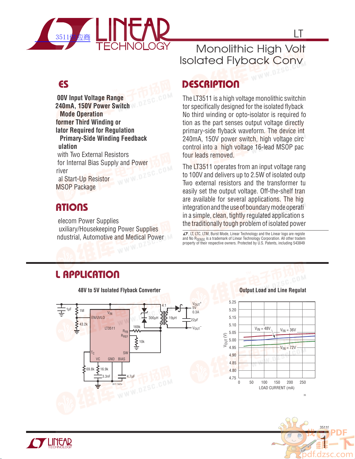
TYPICAL APPLICATION
48V to 5V Isolated Flyback Converter
V
IN
36V TO 72V
1
µF
1M
43.2k
69.8k
V
EN/UVLO
T
IN
LT3511
C
VC GND BIAS
16.9k
3.3nF
3511 TA01a
Output Load and Line Regulation
+
V
22
5V
0.3A
V
OUT
µF
OUT
–
4:1
•
19
µH300µH
169k
R
FB
R
REF
10k
SW
4.7µF
•
(V)
OUT
V
5.25
5.20
5.15
5.10
5.05
5.00
4.95
4.90
4.85
4.80
4.75
VIN = 48V
50
0
100
LOAD CURRENT (mA)
VIN = 36V
VIN = 72V
150 200
250
300
3511 TA01b
3511f
1
LT3511
查询LT3511供应商
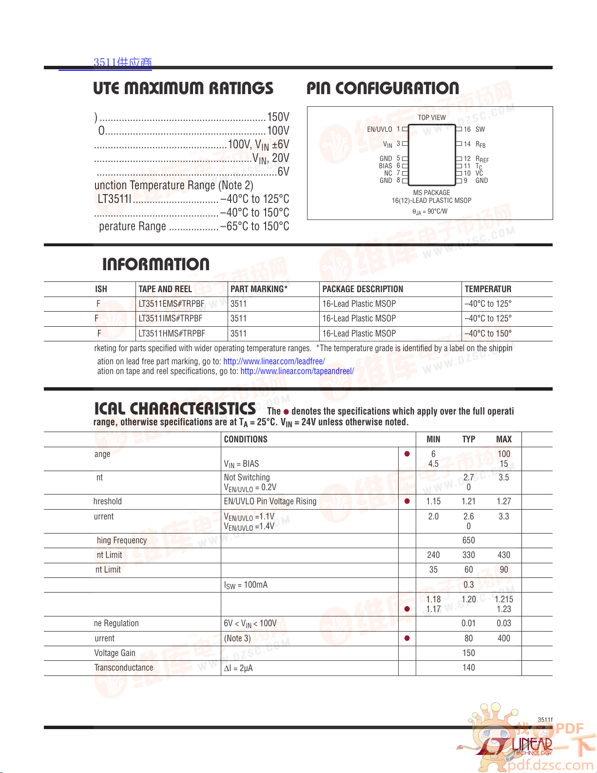
PIN CONFIGURATIONABSOLUTE MAXIMUM RATINGS
(Note 1)
SW (Note 4) ............................................................150V
, EN/UVLO ..........................................................100V
V
IN
............................................................100V, VIN ±6V
R
FB
...................................................................VIN, 20V
BIAS
R
, VC .................................................................6V
REF,TC
Operating Junction Temperature Range (Note 2)
LT3511E, LT3511I ............................... –40°C to 125°C
LT3511H ............................................. –40°C to 150°C
Storage Temperature Range
.................. –65°C to 150°C
EN/UVLO
V
GND
BIAS
NC
GND
IN
TOP VIEW
1
3
5
6
7
8
MS PACKAGE
16(12)-LEAD PLASTIC MSOP
θJA = 90°C/W
SW
16
R
14
FB
12
R
REF
11
T
C
10
VC
9
GND
ORDER INFORMATION
LEAD FREE FINISH TAPE AND REEL PART MARKING* PACKAGE DESCRIPTION TEMPERATURE RANGE
LT3511EMS#PBF LT3511EMS#TRPBF 3511 16-Lead Plastic MSOP –40°C to 125°C
LT3511IMS#PBF LT3511IMS#TRPBF 3511 16-Lead Plastic MSOP –40°C to 125°C
LT3511HMS#PBF LT3511HMS#TRPBF 3511 16-Lead Plastic MSOP –40°C to 150°C
Consult LTC Marketing for parts specified with wider operating temperature ranges. *The temperature grade is identified by a label on the shipping container.
For more information on lead free part marking, go to: http://www.linear.com/leadfree/
For more information on tape and reel specifications, go to: http://www.linear.com/tapeandreel/
ELECTRICAL CHARACTERISTICS
The l denotes the specifications which apply over the full operating
temperature range, otherwise specifications are at TA = 25°C. VIN = 24V unless otherwise noted.
PARAMETER CONDITIONS MIN TYP MAX UNITS
l
Input Voltage Range
Quiescent Current Not Switching
EN/UVLO Pin Threshold EN/UVLO Pin Voltage Rising
EN/UVLO Pin Current V
Maximum Switching Frequency 650 kHz
Maximum Current Limit 240 330 430 mA
Minimum Current Limit 35 60 90 mA
Switch V
CESAT
Voltage
R
REF
Voltage Line Regulation 6V < V
R
REF
Pin Bias Current (Note 3)
R
REF
Error Amplifier Voltage Gain 150 V/V
Error Amplifier Transconductance
= BIAS
V
IN
V
= 0.2V
EN/UVLO
=1.1V
EN/UVLO
V
=1.4V
EN/UVLO
ISW = 100mA 0.3 V
< 100V 0.01 0.03 %/V
IN
∆I = 2µA
6
4.5
2.7
0
l
1.15 1.21 1.27 V
l
l
2.0 2.6
1.18
1.17
0
1.20 1.215
80 400 nA
140 μmhos
100
15
3.5 mA
μA
3.3 μA
μA
1.23
V
V
V
V
2
3511f
V
(V)
查询LT3511供应商
ELECTRICAL CHARACTERISTICS
The l denotes the specifications which apply over the full operating
LT3511
temperature range, otherwise specifications are at TA = 25°C. VIN = 24V unless otherwise noted.
PARAMETER CONDITIONS MIN TYP MAX UNITS
Minimum Switching Frequency 40 kHz
Current into R
T
C
REF
BIAS Pin Voltage Internally Regulated 3 3.1 3.2 V
RTC = 53.6k 9.5 μA
Note 1: Stresses beyond those listed under Absolute Maximum Ratings
may cause permanent damage to the device. Exposure to any Absolute
Maximum Rating condition for extended periods may affect device
reliability and lifetime.
Note 2: The LT3511E is guaranteed to meet performance specifications
from 0°C to 125°C junction temperature. Specifications over the –40°C
to 125°C operating junction temperature range are assured by design,
characterization and correlation with statistical process controls. The
125°C operating junction temperature range. The LT3511H is guaranteed
over the full –40°C to 150°C operating junction temperature range. High
junction temperatures degrade operating lifetimes. Operating lifetime is
derated at junction temperatures greater than 125°C.
Note 3: Current flows out of the R
Note 4: The SW pin is rated to 150V for transients. Operating waveforms
of the SW pin should keep the pedestal of the flyback waveform below
100V as shown in Figure 5.
LT3511I is guaranteed to meet performance specifications from –40°C to
= 25°C, unless otherwise noted.
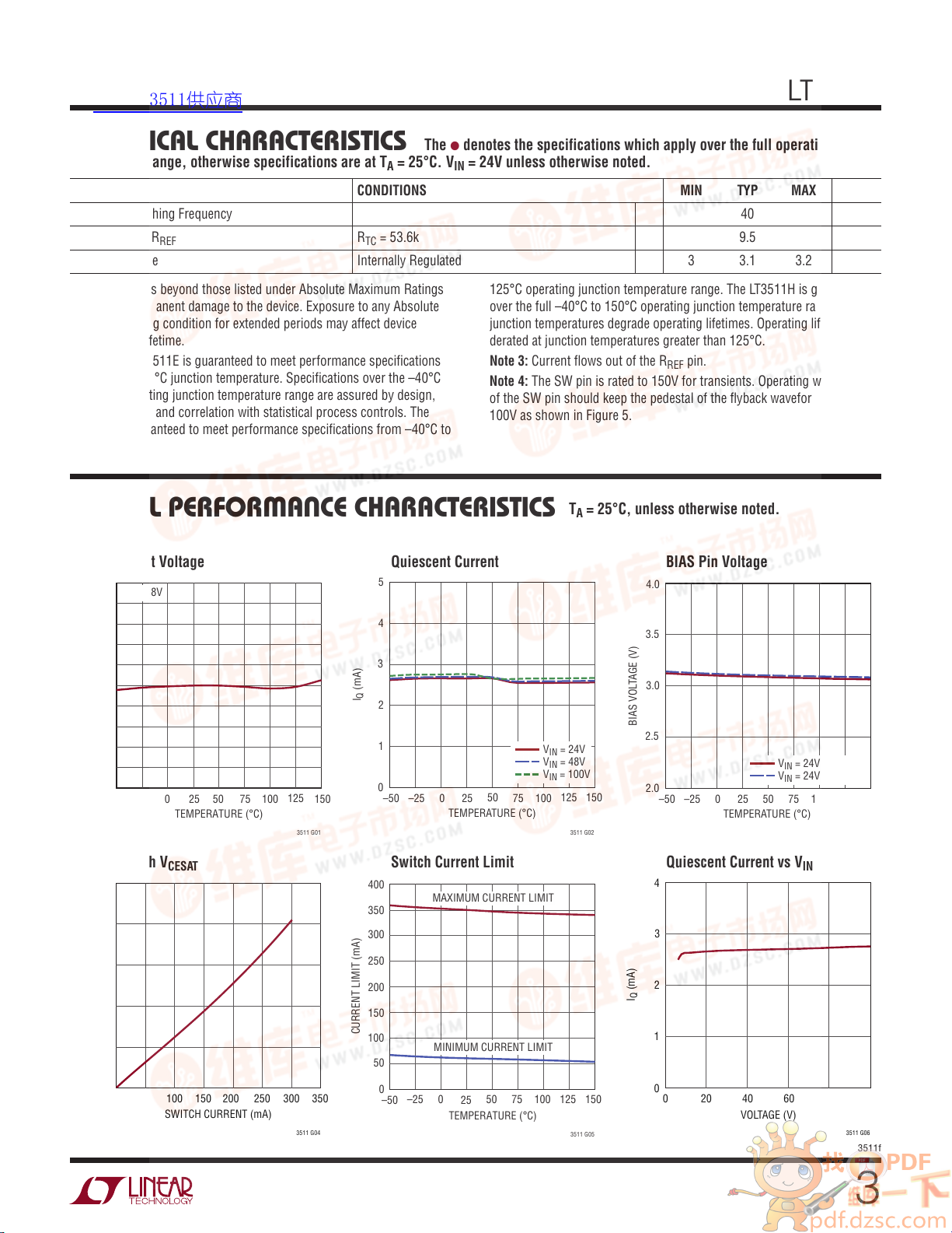
TYPICAL PERFORMANCE CHARACTERISTICS
T
A
Output Voltage Quiescent Current BIAS Pin Voltage
5
4
3
(mA)
Q
I
2
1
0
–50 –25
0
Switch Current Limit
400
350
300
MAXIMUM CURRENT LIMIT
50
25
TEMPERATURE (°C)
75
VIN = 24V
= 48V
V
IN
= 100V
V
IN
100
3511 G02
4.0
3.5
3.0
BIAS VOLTAGE (V)
2.5
150125
2.0
–50
4
3
OUT
1000
5.25
5.20
5.15
5.10
5.05
5.00
4.95
4.90
4.85
4.80
4.75
800
VIN = 48V
–50
–25 25
Switch V
0
50
TEMPERATURE (°C)
CESAT
125
100
75
150
3511 G01
pin.
REF
VIN = 24V, 10mA
= 24V, NO LOAD
V
IN
–25 0 25 50
TEMPERATURE (°C)
75 100 150125
Quiescent Current vs V
3511 G03
IN
600
VOLTAGE (mV)
400
CESAT
200
SWITCH V
0
0 50
150
200
250
100
SWITCH CURRENT (mA)
300
3511 G04
350
250
200
150
CURRENT LIMIT (mA)
100
50
0
–50
MINIMUM CURRENT LIMIT
–25 0 50
25
TEMPERATURE (°C)
75 100 150125
3511 G05
(mA)
Q
I
2
1
0
20
0
40
VOLTAGE (V)
60
80
100
3511 G06
3511f
3
LT3511
查询LT3511供应商
TYPICAL PERFORMANCE CHARACTERISTICS
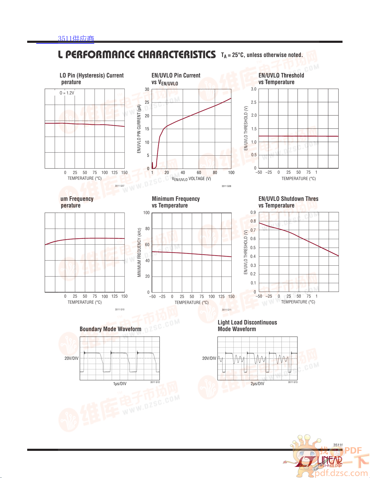
EN/UVLO Pin (Hysteresis) Current
vs Temperature
5
EN/UVLO = 1.2V
4
3
2
EN/UVLO PIN CURRENT (µA)
1
0
–50 –25
0
50
25
TEMPERATURE (°C)
75
100
Maximum Frequency
vs Temperature
1000
800
600
400
MAXIMUM FREQUENCY (kHz)
200
0
–50 –25
0
50
25
TEMPERATURE (°C)
75
100
150125
3511 G07
150125
3511 G10
EN/UVLO Pin Current
vs V
EN/UVLO
30
25
20
15
10
EN/UVLO PIN CURRENT (µA)
5
0
1
20 40 60 80
V
EN/UVLO
Minimum Frequency
vs Temperature
100
80
60
40
MINIMUM FREQUENCY (kHz)
20
0
–50 –25
0
25
TEMPERATURE (°C)
VOLTAGE (V)
50
75
100
TA = 25°C, unless otherwise noted.
EN/UVLO Threshold
vs Temperature
3.0
2.5
2.0
1.5
1.0
EN/UVLO THRESHOLD (V)
0.5
3511 G08
100
0
–50
–25 0
50 100 150125
25 75
TEMPERATURE (°C)
EN/UVLO Shutdown Threshold
vs Temperature
0.9
0.8
0.7
0.6
0.5
0.4
0.3
EN/UVLO THRESHOLD (V)
0.2
0.1
3511 G11
0
150125
–50
–25
0
25 150125
50
TEMPERATURE (°C)
3511 G09
75 100
3511 G14
4
Boundary Mode Waveform
20V/DIV
1µs/DIV
3511 G12
Light Load Discontinuous
Mode Waveform
20V/DIV
2µs/DIV
3511 G13
3511f
查询LT3511供应商
PIN FUNCTIONS
LT3511
EN/UVLO (Pin 1): Enable/Undervoltage Lockout. The EN/
UVLO pin is used to start up the LT3511. Pull the pin to 0V
to shut down the LT3511. This pin has an accurate 1.21V
threshold and can be used to program an undervoltage
lockout (UVLO) threshold using a resistor divider from
supply to ground. A 2.6μA pin current hysteresis allows
the programming of undervoltage lockout (UVLO) hys-
teresis. EN/UVLO can be directly connected to V
. If left
IN
open circuit the part will not power up.
(Pin 3): Input Supply Pin. This pin supplies current to
V
IN
the internal start-up circuitry, and serves as a reference
voltage for the DCM comparator and feedback circuitry.
Must be locally bypassed with a capacitor.
GND (Pin 5, 8, 9): Ground Pins. All three pins should be
tied directly to the local ground plane.
BIAS (Pin 6): Bias Voltage. This pin supplies current to
the switch driver and internal circuitry of the LT3511.
This pin may also be connected to V
is not used and if V
to 4.5V when BIAS and V
< 20V. The part can operate down
IN
are connected together. If a
IN
if a third winding
IN
third winding is used, the BIAS voltage should be lower
than the input voltage and greater than 3.3V for proper
operation. BIAS must be bypassed with a 4.7µF capacitor
placed close to the pin.
VC (Pin 10): Compensation Pin for Internal Error Amplifier.
Connect a series RC from this pin to ground to compensate
the switching regulator. An additional 100pF capacitor from
this pin to ground helps eliminate noise.
(Pin 11): Output Voltage Temperature Compensa-
T
C
tion. Connect a resistor to ground to produce a current
proportional to absolute temperature to be sourced into
REF
node.
the R
ITC = 0.55V/RTC.
(Pin 12): Input Pin for External Ground-Referred
R
REF
Reference Resistor. The resistor at this pin should be 10k.
For nonisolated applications, a traditional resistor voltage
divider from V
(Pin 14): Input Pin for External Feedback Resistor.
R
FB
This pin is connected to the transformer primary (V
The ratio of this resistor to the R
may be connected to this pin.
OUT
resistor, times the
REF
SW
).
internal bandgap reference, determines the output voltage (plus the effect of any non-unity transformer turns
ratio). For nonisolated applications, this pin should be
connected to V
IN
.
SW (Pin 16): Switch Pin. Collector of the internal power
switch. Minimize trace area at this pin to minimize EMI
and voltage spikes.
3511f
5
LT3511
查询LT3511供应商
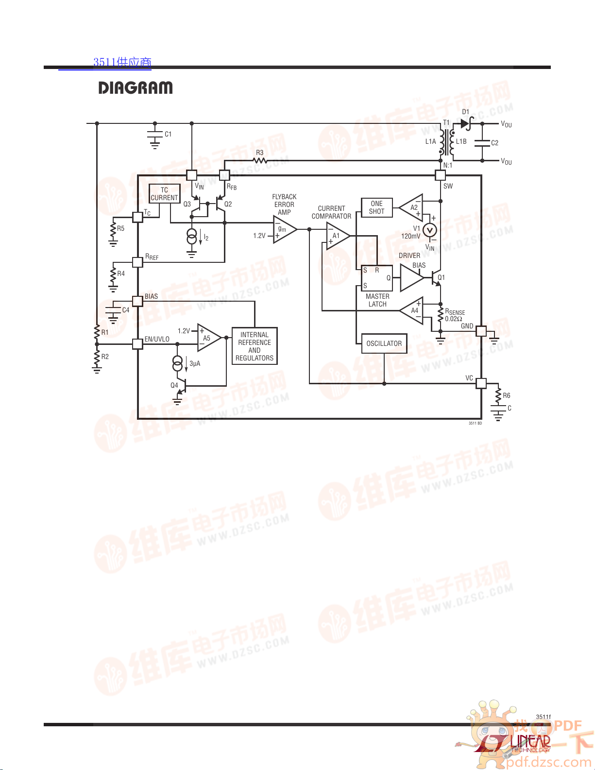
BLOCK DIAGRAM
Q1
T1
N:1
SW
R
SENSE
0.02Ω
D1
GND
V
C
3511 BD
V
IN
C1
R3
TC
CURRENT
T
C
R5
R
REF
R4
BIAS
C4
R1
R2
EN/UVLO
V
Q3
1.2V
3µA
Q4
R
IN
+
–
FB
Q2
I
2
A5
INTERNAL
REFERENCE
REGULATORS
AND
1.2V
FLYBACK
ERROR
AMP
–
g
m
+
CURRENT
COMPARATOR
–
A1
+
ONE
SHOT
RQS
S
MASTER
LATCH
OSCILLATOR
A2
120mV
DRIVER
BIAS
A4
L1A L1B
–
+
+
V1
–
V
IN
+
–
+
V
OUT
C2
–
V
OUT
R6
C3
6
3511f
查询LT3511供应商
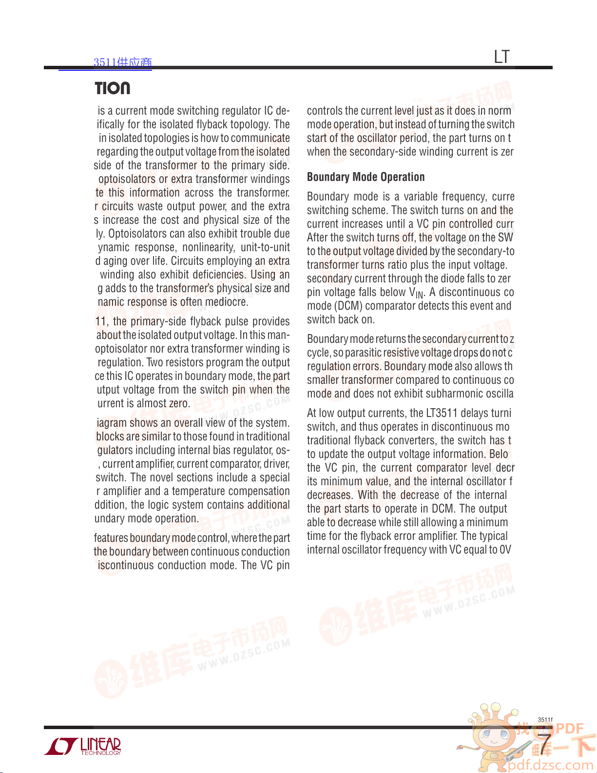
OPERATION
LT3511
The LT3511 is a current mode switching regulator IC de-
signed specifically for the isolated flyback topology. The
key problem in isolated topologies is how to communicate
information regarding the output voltage from the isolated
secondary side of the transformer to the primary side.
Historically, optoisolators or extra transformer windings
communicate this information across the transformer.
Optoisolator circuits waste output power, and the extra
components increase the cost and physical size of the
power supply. Optoisolators can also exhibit trouble due
to limited dynamic response, nonlinearity, unit-to-unit
variation and aging over life. Circuits employing an extra
transformer winding also exhibit deficiencies. Using an
extra winding adds to the transformer’s physical size and
cost, and dynamic response is often mediocre.
In the LT3511, the primary-side flyback pulse provides
information about the isolated output voltage. In this man-
ner, neither optoisolator nor extra transformer winding is
required for regulation. Two resistors program the output
voltage. Since this IC operates in boundary mode, the part
calculates output voltage from the switch pin when the
secondary current is almost zero.
The Block Diagram shows an overall view of the system.
Many of the blocks are similar to those found in traditional
switching regulators including internal bias regulator, os-
cillator, logic, current amplifier, current comparator, driver,
and output switch. The novel sections include a special
flyback error amplifier and a temperature compensation
circuit. In addition, the logic system contains additional
logic for boundary mode operation.
The LT3511 features boundary mode control, where the part
operates at the boundary between continuous conduction
mode and discontinuous conduction mode. The VC pin
controls the current level just as it does in normal current
mode operation, but instead of turning the switch on at the
start of the oscillator period, the part turns on the switch
when the secondary-side winding current is zero.
Boundary Mode Operation
Boundary mode is a variable frequency, current mode
switching scheme. The switch turns on and the inductor
current increases until a VC pin controlled current limit.
After the switch turns off, the voltage on the SW pin rises
to the output voltage divided by the secondary-to-primary
transformer turns ratio plus the input voltage. When the
secondary current through the diode falls to zero, the SW
pin voltage falls below V
mode (DCM) comparator detects this event and turns the
switch back on.
Boundary mode returns the secondary current to zero every
cycle, so parasitic resistive voltage drops do not cause load
regulation errors. Boundary mode also allows the use of a
smaller transformer compared to continuous conduction
mode and does not exhibit subharmonic oscillation.
At low output currents, the LT3511 delays turning on the
switch, and thus operates in discontinuous mode. Unlike
traditional flyback converters, the switch has to turn on
to update the output voltage information. Below 0.6V on
the VC pin, the current comparator level decreases to
its minimum value, and the internal oscillator frequency
decreases. With the decrease of the internal oscillator,
the part starts to operate in DCM. The output current is
able to decrease while still allowing a minimum switch off
time for the flyback error amplifier. The typical minimum
internal oscillator frequency with VC equal to 0V is 40kHz.
. A discontinuous conduction
IN
3511f
7

LT3511
查询LT3511供应商
APPLICATIONS INFORMATION
PSUEDO DC THEORY
In the Block Diagram, R
(R4) and RFB (R3) are external
REF
resistors used to program the output voltage. The LT3511
operates similar to traditional current mode switchers,
except in the use of a unique error amplifier, which derives
its feedback information from the flyback pulse.
Operation is as follows: when the output switch, Q1, turns
off, its collector voltage rises above the V
rail. The am-
IN
plitude of this flyback pulse, i.e., the difference between
it and V
V
, is given as:
IN
= (V
FLBK
OUT
+ VF + I
• ESR) • N
SEC
PS
VF = D1 forward voltage
= Transformer secondary current
I
SEC
ESR = Total impedance of secondary circuit
= Transformer effective primary-to-secondary turns
N
PS
ratio
and Q2 convert the flyback voltage into a current. Nearly
R
FB
all of this current flows through R
to form a ground-
REF
referred voltage. The resulting voltage forms the input
to the flyback error amplifier. The flyback error amplifier
samples the voltage information when the secondary side
winding current is zero. The bandgap voltage, 1.20V, acts
as the reference for the flyback error amplifier.
the effect of nonzero secondary output impedance (ESR).
Boundary control mode minimizes the effect of this impedance term.
Temperature Compensation
The first term in the V
equation does not have tem-
OUT
perature dependence, but the diode forward drop has a
significant negative temperature coefficient. A positive
temperature coefficient current source connects to the
pin to compensate. A resistor to ground from the
R
REF
pin sets the compensation current.
T
C
The following equation explains the cancellation of the
temperature coefficient:
dV
dT
R
TC
R
F
= −
=
−R
N
R
FB
TC
FB
PS
1
dV
•
N
PS
1
•
dV
/ dT
F
TC
•
or,
dT
dV
•
dT
TC
R
FB
≈
N
PS
(dVF/dT) = Diode’s forward voltage temperature coefficient
/dT) = 2mV
(dV
TC
= 0.55V
V
TC
Experimentally verify the resulting value of R
and adjust as
TC
necessary to achieve optimal regulation over temperature.
The relatively high gain in the overall loop will then cause
the voltage at R
reference voltage V
and VBG approximately equals:
V
FLBK
V
FL BK
R
FB
=
to be nearly equal to the bandgap
REF
. The resulting relationship between
BG
V
BG
or V
R
RE F
FL BK
= V
BG
R
FB
R
RE F
VBG = Internal bandgap reference
Combination of the preceding expression with earlier
derivation of V
V
= V
OU T
The expression defines V
results in the following equation:
FLBK
1
N
PS
in terms of the internal ref-
OUT
− V
− I
F
BG
R
FB
R
RE F
SE C
(ESR)
erence, programming resistors, transformer turns ratio
and diode forward voltage drop. Additionally, it includes
8
The addition of a temperature coefficient current modifies
the expression of output voltage as follows:
FB
PS
1
− V
F
N
PS
– I
SE C
(ESR)
V
= V
OU T
BG
V
−
R
TC
TC
R
FB
R
RE F
R
•
N
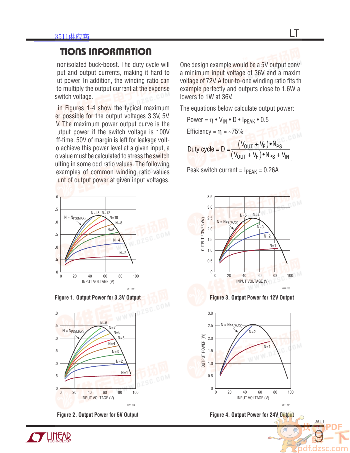
Output Power
A flyback converter has a complicated relationship between the input and output current compared to a buck
or a boost. A boost has a relatively constant maximum
input current regardless of input voltage and a buck has a
relatively constant maximum output current regardless of
input voltage. This is due to the continuous nonswitching
behavior of the two currents. A flyback converter has both
discontinuous input and output currents which makes it
3511f
( )
查询LT3511供应商
APPLICATIONS INFORMATION
LT3511
similar to a nonisolated buck-boost. The duty cycle will
affect the input and output currents, making it hard to
predict output power. In addition, the winding ratio can
be changed to multiply the output current at the expense
of a higher switch voltage.
The graphs in Figures 1-4 show the typical maximum
output power possible for the output voltages 3.3V, 5V,
12V and 24V. The maximum power output curve is the
calculated output power if the switch voltage is 100V
during the off-time. 50V of margin is left for leakage volt-
age spike. To achieve this power level at a given input, a
winding ratio value must be calculated to stress the switch
to 100V, resulting in some odd ratio values. The following
curves are examples of common winding ratio values
and the amount of output power at given input voltages.
3.0
2.5
N = N
2.0
1.5
1.0
OUTPUT POWER (W)
0.5
PS(MAX)
N = 15
N = 12
N = 10
N = 8
N = 6
N = 4
N = 2
One design example would be a 5V output converter with
a minimum input voltage of 36V and a maximum input
voltage of 72V. A four-to-one winding ratio fits this design
example perfectly and outputs close to 1.6W at 72V but
lowers to 1W at 36V.
The equations below calculate output power:
Power = η • VIN • D • I
PEAK
• 0.5
Efficiency = η = ~75%
+ V
V
Duty cycle = D =
OUT
V
( )
OUT
Peak switch current = I
3.5
3.0
2.5
N = N
2.0
1.5
OUTPUT POWER (W)
1.0
0.5
N = 5
PS(MAX)
+ V
PEAK
F
• NPS+ V
F
= 0.26A
N = 4
N = 3
N = 2
• N
N = 1
PS
IN
0
0
20 40 60 80
INPUT VOLTAGE (V)
3511 F01
Figure 1. Output Power for 3.3V Output
3.0
2.5
N = N
PS(MAX)
2.0
1.5
1.0
OUTPUT POWER (W)
0.5
0
0
20 40 60 80
INPUT VOLTAGE (V)
N = 8
N = 7
N = 6
N = 5
N = 4
N = 3
N = 2
N = 1
3511 F02
Figure 2. Output Power for 5V Output
100
100
0
20 40 60 80
0
INPUT VOLTAGE (V)
3511 F05
Figure 3. Output Power for 12V Output
3.0
N = N
2.5
2.0
1.5
1.0
OUTPUT POWER (W)
0.5
0
PS(MAX)
0
20 40 60 80
INPUT VOLTAGE (V)
N = 2
N = 1
3511 F04
Figure 4. Output Power for 24V Output
100
100
3511f
9

LT3511
查询LT3511供应商
APPLICATIONS INFORMATION
TRANSFORMER DESIGN CONSIDERATIONS
Successful application of the LT3511 relies on proper
transformer specification and design. Carefully consider
the following information in addition to the traditional
Linear Technology has worked with several leading magnetic component manufacturers to produce pre-designed
flyback transformers for use with the LT3511. Table 1
shows the details of these transformers.
guidelines associated with high frequency isolated power
supply transformer design.
Table 1. Predesigned Transformers
TRANSFORMER
PART NUMBER L
750311558 300 1.5 4:1:1 1500 500 Würth Elektronik 48V to 5V, 0.3A
750311019 400 5 6:1:2 1500 750 Würth Elektronik 24V to 5V, 0.26A
750311659 300 2 1:1:0.2 1500 560 Würth Elektronik 48V to 24V, 0.07A
750311660 350 3 2:1:0.33 1500 520 Würth Elektronik 48V to 15V, 0.13A
750311838 350 3 2:1:1 1500 520 Würth Elektronik 48V to ±15V, 0.055A
750311963 200 0.4 1:5:5 1500 650 Würth Elektronik 12V to ±70V, 0.005A
750311966 120 0.45 1:5:0.5 1500 900 Würth Elektronik 12V to +120V and
10396-T024 300 2.0 4:1:1 1500 500 Sumida 48V to 5V, 0.3A
10396-T026 300 2.5 6:1:2 1500 500 Sumida 24V to 5V, 0.26A
01355-T057 250 2.0 1:1:0.2 1500 500 Sumida 48V to 24V, 0.07A
10396-T022 300 2.0 2:1:0.33 1500 500 Sumida 48V to 15V, 0.13A
10396-T028 300 2.5 2:1:1 1500 500 Sumida 48V to ±15V, 0.055A
(µH) LEAKAGE (µH) NP:NS:N
PRI
B
ISOLATION (V)
SATURATION
CURRENT (mA) VENDOR
TARGET
APPLICATIONS
24V to 5V, 0.2A
12V to 5V, 0.15A
48V to 3.3V, 0.33A
24V to 3.3V, 0.28A
12V to 3.3V, 0.18A
12V to 5V, 0.17A
48V to 3.3V, 0.43A
24V to 3.3V, 0.35A
12V to 3.3V, 0.21A
48V to 12V, 0.14A
24V to 15V, 0.1A
12V to 15V, 0.058A
48V to ±12V, 0.07A
24V to ±15V, 0.045A
12V to ±100V, 0.004A
12V to ±150V, 0.003A
–12V, 0.005A
24V to 5V, 0.2A
12V to 5V, 0.15A
48V to 3.3V, 0.33A
24V to 3.3V, 0.28A
12V to 3.3V, 0.18A
12V to 5V, 0.17A
48V to 3.3V, 0.43A
24V to 3.3V, 0.35A
12V to 3.3V, 0.21A
48V to 12V, 0.14A
24V to 15V, 0.1A
12V to 15V, 0.058A
48V to ±12V, 0.07A
24V to ±15V, 0.045A
3511f
10
150V – V
– V
( )
查询LT3511供应商
APPLICATIONS INFORMATION
LT3511
Turns Ratio
Note that when using an R
FB/RREF
resistor ratio to set
output voltage, the user has relative freedom in selecting
a transformer turns ratio to suit a given application. In
contrast, the use of simple ratios of small integers, e.g.,
1:1, 2:1, 3:2, provides more freedom in setting total turns
and mutual inductance.
Typically, choose the transformer turns to maximize avail-
able output power. For low output voltages (3.3V or 5V), a
N:1 turns ratio can be used with multiple primary windings
relative to the secondary to maximize the transformer’s
current gain (and output power). However, remember that
the SW pin sees a voltage that is equal to the maximum
input supply voltage plus the output voltage multiplied by
the turns ratio. In addition, leakage inductance will cause
a voltage spike (V
LEAKAGE
) on top of this reflected voltage.
This total quantity needs to remain below the absolute
maximum rating of the SW pin to prevent breakdown of
the internal power switch. Together these conditions place
an upper limit on the turns ratio, N, for a given application.
Choose a turns ratio low enough to ensure:
N <
IN(MAX )
V
OU T
+ V
LEAK AGE
F
For larger N:1 values, a transformer with a larger physical
size is needed to deliver additional current and provide a
large enough inductance value to ensure that the off-time
is long enough to accurately measure the output voltage.
For larger N:1 values, choose a transformer with a larger
physical size to deliver additional current. In addition,
choose a large enough inductance value to ensure that
the off-time is long enough to measure the output voltage.
For lower output power levels, choose a 1:1 or 1:N
transformer for the absolute smallest transformer size. A
1:N transformer will minimize the magnetizing inductance
(and minimize size), but will also limit the available output
power. A higher 1:N turns ratio makes it possible to have
very high output voltages without exceeding the breakdown
voltage of the internal power switch.
The turns ratio is an important element in the isolated
feedback scheme. Make sure the transformer manufacturer
guarantees turns ratio accuracy within ±1%.
Saturation Current
The current in the transformer windings should not exceed its rated saturation current. Energy injected once the
core is saturated will not be transferred to the secondary
and will instead be dissipated in the core. Information on
saturation current should be provided by the transformer
manufacturers. Table 1 lists the saturation current of the
transformers designed for use with the LT3511.
Primary Inductance Requirements
The LT3511 obtains output voltage information from the
reflected output voltage on the switch pin. The conduction
of secondary winding current reflects the output voltage
on the primary. The sampling circuitry needs a minimum
of 400ns to settle and sample the reflected output voltage.
In order to ensure proper sampling, the secondary winding
needs to conduct current for a minimum of 400ns. The
following equation gives the minimum value for primaryside magnetizing inductance:
L
PRI
t
OFF(MIN)
I
PEAK(MIN)
t
OFF(MIN)
≥
= 400ns
= 55mA
• NPS• V
I
PEAK(MIN)
OUT
+ V
F
Leakage Inductance and Clamp Circuits
Transformer leakage inductance (on either the primary or
secondary) causes a voltage spike to appear at the primary
after the output switch turns off. This spike is increasingly
prominent at higher load currents where more stored energy must be dissipated. When designing an application,
adequate margin should be kept for the effect of leakage
voltage spikes. In most cases the reflected output voltage
on the primary plus V
should be kept below 100V. This
IN
leaves at least 50V of margin for the leakage spike across
line and load conditions. A larger voltage margin will be
needed for poorly wound transformers or for excessive
leakage inductance. Figure 5 illustrates this point. Minimize
transformer leakage inductance.
A clamp circuit is recommended for most applications.
3511f
11

LT3511
查询LT3511供应商
APPLICATIONS INFORMATION
V
SW
<150V
V
LEAKAGE
<100V
t
> 400ns
OFF
t
< 150ns
SP
without Clamp
Figure 5. Maximum Voltages for SW Pin Flyback Waveform
TIME
Two circuits that can protect the internal power switch
include the RCD (resistor-capacitor-diode) clamp and the
DZ (diode-Zener) clamp. The clamp circuits dissipate the
stored energy in the leakage inductance. The DZ clamp
is the recommended clamp for the LT3511. Simplicity of
design, high clamp voltages, and low power levels make the
DZ clamp the preferred solution. Additionally, a DZ clamp
ensures well defined and consistent clamping voltages.
Figure 5 shows the clamp effect on the switch waveform
and Figure 6 shows the connection of the DZ clamp.
Proper care must be taken when choosing both the diode
and the Zener diode. Schottky diodes are typically the best
choice, but some PN diodes can be used if they turn on
fast enough to limit the leakage inductance spike. Choose
a diode that has a reverse-voltage rating higher than the
maximum input voltage. The Zener diode breakdown volt-
age should be chosen to balance power loss and switch
voltage protection. The best compromise is to choose the
largest voltage breakdown. Use the following equation to
make the proper choice:
V
ZENER(MAX)
≤ 150V – V
IN(MAX)
For an application with a maximum input voltage of 72V,
choose a 68V V
ZENER
which has V
ZENER(MAX)
at 72V, which
will be below the 78V maximum.
The power loss in the clamp will determine the power rat-
ing of the Zener diode. Power loss in the clamp is highest
at maximum load and minimum input voltage. The switch
V
SW
<150V
<140V
<100V
t
> 400ns
OFF
TIME
t
SP
< 150ns
with Clamp
Z
D
Figure 6. DZ Clamp
3511 F05
L
S
3511 F06
current is highest at this point along with the energy stored
in the leakage inductance. A 0.5W Zener will satisfy most
applications when the highest V
a low value for V
will cause excessive power loss as
ZENER
is chosen. Choosing
ZENER
shown in the following equations:
DZ Power Loss=
1
• L•I
2
1+
PK( VIN(MIN))
N
PS
V
ZENER–NPS
2
• fSW•
• V
+ V
( )
OUT
• V
( )
OUT
+ V
F
F
L = Leakage Inductance
I
PK( VIN(MIN))
fSW=
tON+ t
V
OFF
OUT•IOUT
η • V
IN(MIN)
=
L
PRI•IPK( VIN(MIN))
=
1
• D
V
IN(MIN)
• 2
VIN(MIN)
1
L
PRI•IPK( VIN(MIN))
+
NPS• V
( )
OUT
+ V
F
12
3511f

查询LT3511供应商
APPLICATIONS INFORMATION
LT3511
Table 2 and 3 show some recommended diodes and Zener
diodes.
Table 2. Recommended Zener Diodes
V
ZENER
PART
MMSZ5266BT1G 68 0.5 SOD-123 On Semi
MMSZ5270BT1G 91 0.5 SOD-123
CMHZ5266B 68 0.5 SOD-123 Central
CMHZ5267B 75 0.5 SOD-123
BZX84J-68 68 0.5 SOD323F NXP
BZX100A 100 0.5 SOD323F
Table 3. Recommended Diodes
PART I (A)
BAV19W 0.625 100 SOD-123 Diodes Inc.
BAV20W 0.625 150 SOD-123
(V)
POWER
(W) CASE VENDOR
Semiconductor
V
REVERSE
(V) CASE VENDOR
Leakage Inductance Blanking
When the power switch turns off, the flyback pulse ap-
pears. However, a finite time passes before the trans-
former primary-side voltage waveform approximately
represents the output voltage. Rise time on the SW node
and transformer leakage inductance cause the delay. The
leakage inductance also causes a very fast voltage spike
on the primary side of the transformer. The amplitude of
the leakage spike is largest when power switch current is
highest. Introduction of an internal fixed delay between
switch turn-off and the start of sampling provides im-
munity to the phenomena discussed above. The LT3511
sets internal blanking to 150ns. In certain cases leakage
inductance spikes last longer than the internal blanking,
but will not significantly affect output regulation.
Secondary Leakage Inductance
In addition to primary leakage inductance, secondary leak-
age inductance exhibits an important effect on application
design. Secondary leakage inductance forms an inductive
divider on the transformer secondary. The inductive divider
effectively reduces the size of the primary-referred flyback
pulse. The smaller flyback pulse results in a higher regulated
output voltage. The inductive divider effect of secondary
leakage inductance is load independent. R
FB/RREF
ratio
adjustments can accommodate this effect to the extent
secondary leakage inductance is a constant percentage
of mutual inductance (over manufacturing variations).
Winding Resistance Effects
Resistance in either the primary or secondary will reduce
overall efficiency (P
OUT/PIN
). Good output voltage regulation will be maintained independent of winding resistance
due to the boundary mode operation of the LT3511.
Bifilar Winding
A bifilar, or similar winding technique, is a good way to
minimize troublesome leakage inductances. However, remember that this will also increase primary-to-secondary
capacitance and limit the primary-to-secondary breakdown
voltage, so bifilar winding is not always practical. The
Linear Technology applications group is available and
extremely qualified to assist in the selection and/or design
of the transformer.
APPLICATION DESIGN CONSIDERATIONS
Iterative Design Process
The LT3511 uses a unique sampling scheme to regulate
the isolated output voltage. The use of this isolated scheme
requires a simple iterative process to choose feedback
resistors and temperature compensation. Feedback resistor values and temperature compensation resistance
is heavily dependent on the application, transformer and
output diode chosen.
Once resistor values are fixed after iteration, the values
will produce consistent output voltages with the chosen
transformer and output diode. Remember, the turns ratio
of the transformer must be guaranteed within ±1%. The
transformer vendors mentioned in this data sheet can
build transformers to this specification.
3511f
13

LT3511
( )
R2
查询LT3511供应商
APPLICATIONS INFORMATION
Selecting RFB and R
Resistor Values
REF
The following section provides an equation for setting
R
FB
and R
values. The equation should only serve
REF
as a guide. Follow the procedure outlined in the Design
, R
Procedure to set accurate values for R
FB
and RTC
REF
using the iterative design procedure.
Rearrangement of the expression for V
in the Tempera-
OUT
ture Compensation section, developed in the Operations
section, yields the following expression for R
• N
PSVOU T
+ V
+ V
F
TC
V
BG
RFB=
R
RE F
:
FB
where:
V
= Output voltage
OUT
VF = Switching diode forward voltage
NPS = Effective primary-to-secondary turns ratio
VTC = 0.55V
This equation assumes:
R
RTC=
FB
N
PS
The equation assumes the temperature coefficients of
the diode and V
are equal, which is a good first order
TC
approximation.
Strictly speaking, the above equation defines R
absolute value, but as a ratio of R
is, what is the proper value for R
should be approximately 10k. The LT3511 is trimmed
R
REF
and specified using this value of R
varies considerably from 10k, additional errors will
R
REF
result. However, a variation in R
. So the next question
REF
? The answer is that
REF
. If the impedance of
REF
of several percent is
REF
not as an
FB
acceptable. This yields a bit of freedom in selecting stan-
dard 1% resistor values to yield nominal R
FB/RREF
ratios.
Undervoltage Lockout (UVLO)
A resistive divider from V
to the EN/UVLO pin imple-
IN
ments undervoltage lockout (UVLO). Figure 7 shows this
configuration. The EN/UVLO pin threshold is set at 1.21V.
V
IN
R1
EN/UVLO
LT3511
GND
Figure 7. Undervoltage Lockout (UVLO)
R2
RUN/STOP
CONTROL
(OPTIONAL)
3511 F07
In addition, the EN/UVLO pin draws 2.6µA when the voltage at the pin is below 1.21V. This current provides user
programmable hysteresis based on the value of R1. The
effective UVLO thresholds are:
V
IN(UVLO,RISING)
V
IN(UVLO,FA L L ING)
1.2V • (R1+ R2)
=
R2
1.2V • (R1+ R2)
=
+ 2.6µA • R1
Figure 7 also shows the implementation of external shutdown control while still using the UVLO function. The
NMOS grounds the EN/UVLO pin when turned on, and
puts the LT3511 in shutdown with quiescent current draw
of less than 1µA.
Minimum Load Requirement
The LT3511 recovers output voltage information using the
flyback pulse. The flyback pulse occurs once the switch
turns off and the secondary winding conducts current. In
order to regulate the output voltage, the LT3511 needs to
sample the flyback pulse. The LT3511 delivers a minimum
amount of energy even during light load conditions to
ensure accurate output voltage information. The minimum
delivery of energy creates a minimum load requirement
of 10mA to 15mA depending on the specific application.
Verify minimum load requirements for each application.
A Zener diode with a Zener breakdown of 20% higher
than the output voltage can serve as a minimum load if
pre-loading is not acceptable. For a 5V output, use a 6V
Zener with cathode connected to the output.
3511f
14
查询LT3511供应商
APPLICATIONS INFORMATION
LT3511
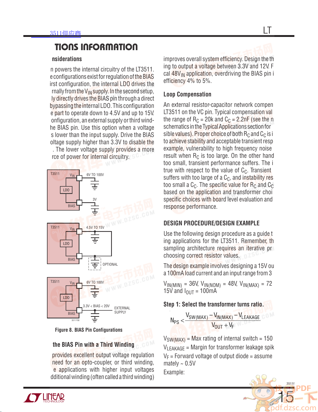
BIAS Pin Considerations
The BIAS pin powers the internal circuitry of the LT3511.
Three unique configurations exist for regulation of the BIAS
pin. In the first configuration, the internal LDO drives the
BIAS pin internally from the V
supply directly drives the BIAS pin through a direct
the V
IN
supply. In the second setup,
IN
connection bypassing the internal LDO. This configuration
will allow the part to operate down to 4.5V and up to 15V.
In the third configuration, an external supply or third wind-
ing drives the BIAS pin. Use this option when a voltage
supply exists lower than the input supply. Drive the BIAS
pin with a voltage supply higher than 3.3V to disable the
internal LDO. The lower voltage supply provides a more
efficient source of power for internal circuitry.
LT3511
V
LDO
BIAS
6V TO 100V
IN
3V
improves overall system efficiency. Design the third winding to output a voltage between 3.3V and 12V. For a typical 48V
application, overdriving the BIAS pin improves
IN
efficiency 4% to 5%.
Loop Compensation
An external resistor-capacitor network compensates the
LT3511 on the VC pin. Typical compensation values are in
the range of R
= 20k and CC = 2.2nF (see the numerous
C
schematics in the Typical Applications section for other possible values). Proper choice of both R
and CC is important
C
to achieve stability and acceptable transient response. For
example, vulnerability to high frequency noise and jitter
result when R
is too large. On the other hand, if RC is
C
too small, transient performance suffers. The inverse is
true with respect to the value of C
suffers with too large of a C
too small a C
. The specific value for RC and CC will vary
C
, and instability results from
C
. Transient response
C
based on the application and transformer choice. Verify
specific choices with board level evaluation and transient
response performance.
LT3511
LT3511
V
LDO
BIAS
V
LDO
BIAS
Figure 8. BIAS Pin Configurations
IN
IN
3511 F08
4.5V TO 15V
OPTIONAL
6V TO 100V
3.3V < BIAS < 20V
EXTERNAL
SUPPLY
Overdriving the BIAS Pin with a Third Winding
The LT3511 provides excellent output voltage regulation
without the need for an opto-coupler, or third winding,
but for some applications with higher input voltages
(>20V), an additional winding (often called a third winding)
DESIGN PROCEDURE/DESIGN EXAMPLE
Use the following design procedure as a guide to designing applications for the LT3511. Remember, the unique
sampling architecture requires an iterative process for
choosing correct resistor values.
The design example involves designing a 15V output with
a 100mA load current and an input range from 36V to 72V.
V
IN(MIN)
= 36V, V
15V and I
= 100mA
OUT
IN(NOM)
= 48V, V
IN(MAX)
= 72V, V
OUT
=
Step 1: Select the transformer turns ratio.
V
NPS<
SW(MAX)
V
SW(MAX)
V
LEAKAGE
= Forward voltage of output diode = assume approxi-
V
F
= Max rating of internal switch = 150V
= Margin for transformer leakage spike = 40V
– V
V
OUT
IN(MAX)
+ V
– V
F
LEAKAGE
mately ~ 0.5V
Example:
3511f
15
LT3511
( )
( )
( )
( )
查询LT3511供应商
APPLICATIONS INFORMATION
150V –72V – 40V
NPS<
15V + 0.5V
NPS< 2.45
= 2
N
PS
The choice of turns ratio is critical in determining output
power as shown earlier in the Output Power section. At
this point, a third winding can be added to the transformer
to drive the BIAS pin of the LT3511 for higher efficiencies.
Choose a turns ratio that sets the third winding voltage
to regulate between 3.3V and 6V for maximum efficiency.
Choose a third winding ratio to drive BIAS winding with
5V. (Optional)
Example:
N
THIRD
N
V
THIRD
=
S
V
OUT
=
5V
15V
= 0.33
The turns ratio of the transformer chosen is as follows
N
PRIMARY
: N
SECONDARY
: N
THIRD
= 2:1:0.33.
Step 2: Calculate maximum power output at minimum
VIN.
P
OUT(VIN(MIN))
I
PEAK
D=
( )
• 0.5
V
OUT
V
+ V
OUT
= η • V
+ V
F
• NPS+ V
F
IN(MIN)
• N
• IIN = η • V
PS
IN(MIN)
IN(MIN)
• D •
η = Efficiency = ~75%
Step 3: Determine primary inductance, switching
frequency and saturation current.
Primary inductance for the transformer must be set
above a minimum value to satisfy the minimum off time
requirement.
L
PRI
t
OFF(MIN)
I
PEAK(MIN)
t
OFF(MIN)
≥
= 400ns
= 55mA
• NPS• V
I
PEAK(MIN)
OUT
+ V
F
Example:
400ns• 2 • 15+ 0.5
L
≥
PRI
L
≥ 225µH
PRI
0.055
In addition, primary inductance will determine switching
frequency.
fSW=
I
PEAK
tON+ t
V
OUT•IOUT
=
1
η • V
OFF
IN
=
L
PRI•IPEAK
• 2
• D
V
IN
1
+
NPS• V
L
PRI•IPEAK
( )
OUT
+ V
F
Example:
Let’s calculate switching frequency at our nominal V
IN
of 48V.
I
= Peak switch current = 0.26A
PEAK
Example:
D = 0.46
P
OUT(VIN(MIN))
I
OUT(VIN(MIN))
= 1.62
= P
OUT(VIN(MIN))/VOUT
= 0.11A
The chosen turns ratio satisfies the output current re-
quirement of 100mA. If the output current was too low,
the minimum input voltage could be adjusted higher. The
turns ratio in this example is set to its highest ratio given
switch voltage requirements and margin for leakage in-
ductance voltage spike.
D=
15+ 0.5
15+ 0.5
( )
I
PEAK
15V • 0.1A • 2
=
0.75 • 48V • 0.39
Let’s choose L
ers specify primary inductance with a tolerance of ±20%.
fSW = 256kHz
Finally, the transformer needs to be rated for the correct
saturation current level across line and load conditions.
In the given example, the worst-case condition for switch
current is at minimum V
• 2
= 0.39
• 2+ 48
= 0.21A
= 350µH. Remember, most transform-
PRI
and maximum load.
IN
3511f
16
0.75 • 36V • 0.46
2
查询LT3511供应商
APPLICATIONS INFORMATION
LT3511
I
PEAK
I
PEAK
V
OUT•IOUT
=
η • V
15V • 0.1A • 2
=
• 2
• D
IN
= 0.24A
Ensure that the saturation current covers steady-state
operation, start-up and transient conditions. To satisfy
these conditions, choose a saturation current 50% or more
higher than the steady-state calculation. In this example, a
saturation current between 400mA and 500mA is chosen.
Table 1 presents a list of pre-designed flyback transform-
ers. For this application, the Würth 750311660 transformer
will be used.
Step 4: Choose the correct output diode.
The two main criteria for choosing the output diode include
forward current rating and reverse voltage rating. The
maximum load requirement is a good first-order guess
at the average current requirement for the output diode.
A better metric is RMS current.
1–D
I
RMS
= I
PEAK(VIN(MIN))
• NPS•
VIN(MIN)
3
Example:
I
= 0.24 • 2 •
RMS
1– 0.46
3
= 0.2A
Next calculate reverse voltage requirement using maxi-
mum V
IN
V
REVERSE
:
V
= V
OUT
+
IN(MAX)
N
PS
Step 5: Choose an output capacitor.
The output capacitor choice should minimize output voltage
ripple and balance the trade-off between size and cost for
a larger capacitor. Use the equation below at nominal V
• D
I
∆V
OUT
OUT
• f
SW
C =
IN
:
Example:
Design for ripple levels below 50mV.
0.1A • 0.39
C =
0.05V • 256kHz
= 3.1µF
A 10µF, 25V output capacitor is chosen. Remember ceramic capacitors lose capacitance with applied voltage.
The capacitance can drop to 40% of quoted capacitance
at the max voltage rating.
Step 6: Design clamp circuit.
The clamp circuit protects the switch from leakage inductance spike. A DZ clamp is the preferred clamp circuit. The
Zener and the diode need to be chosen.
The maximum Zener value is set according to the maximum V
V
:
IN
ZENER(MAX)
≤ 150V – V
IN(MAX)
Example:
V
ZENER(MAX)
V
ZENER(MAX)
≤ 150V – 72V
≤ 78V
In addition, power loss in the clamp circuit is inversely
related to the clamp voltage as shown previously. Higher
clamp voltages lead to lower power loss.
Example:
A 68V Zener with a maximum of 72V will provide optimal
protection and minimize power loss. Half-watt Zeners will
72V
= 51V
V
REVERSE
= 15V +
A 0.5A, 60V diode from Diodes Inc. (SBR0560S1) will
be used.
satisfy most clamp applications involving the LT3511.
Power loss can be calculated using the equations presented
in the Leakage Inductance and Clamp Circuit section.
The Zener chosen is a 68V 0.5W Zener from On Semiconductor (MMSZ5266BT1G).
3511f
17
LT3511
( )
( )
查询LT3511供应商
APPLICATIONS INFORMATION
Choose a diode that is fast and has sufficient reverse
voltage breakdown:
V
REVERSE
> V
IN(MAX)
Example:
V
REVERSE
> 72V
The diode needs to handle the peak switch current of the
switch which was determined to be 0.24A. A 100V, 0.6A
diode from Diodes Inc. (BAV19W) is chosen.
Step 7: Compensation.
Compensation will be optimized towards the end of the
design procedure. Connect a resistor and capacitor from
the VC node to ground. Use a 20k resistor and a 2.2nF
capacitor.
Step 8: Select R
and RTC Resistors.
FB
Use the following equations to choose starting values for
and RTC. Set R
R
FB
RFB=
V
OUT
to 10k.
REF
+ VF+ 0.55V
• NPS• R
REF
1.2V
R
= 10k
REF
R
FB
=
R
TC
N
PS
Example:
RFB=
15+ 0.5 + 0.55V
• 2• 10k
= 267k
1.2V
267k
=
R
TC
= 133k
2
Step 9: Adjust RFB based on output voltage.
Power up the application with application components
connected and measure the regulated output voltage.
Readjust R
R
FB(NEW)
based on the measured output voltage.
FB
V
=
OUT
V
OUT(MEAS)
• R
FB(OLD)
Example:
=
16.8V
15V
• 267k = 237k
R
FB(NEW)
Step 10: Remove RTC and measure output voltage
over temperature.
Measure output voltage in a controlled temperature environment like an oven to determine the output temperature
coefficient. Measure output voltage at a consistent load
current and input voltage, across the temperature range
of operation. This procedure will optimize line and load
regulation over temperature.
Calculate the temperature coefficient of V
∆V
OUT
∆Temp
V
=
OUT(HOT )
T
HOT(°C)
– V
OUT(COLD)
– T
COLD(°C)
OUT
:
Example:
V
measured at 100mA and 48V
OUT
∆V
OUT
∆Temp
15.70V –15.37V
=
125°C– −50°C
( )
IN
= 1.9mV °C
3511f
18
°
( )
查询LT3511供应商
APPLICATIONS INFORMATION
LT3511
Step 11: Calculate new value for RTC.
R
TC(NEW )
=
•
N
PS
∆V
1.85mV
R
FB
∆Temp
C
OUT
Example:
R
TC(NEW )
=
237k
Step 12: Place new value for RTC, measure V
readjust R
R
FB(NEW)
due to RTC change.
FB
=
V
1.85
•
2
1.9
V
OUT
OUT(MEAS)
= 118k
• R
FB(OLD)
OUT
, and
Example:
=
15V
• 237k = 237k
15V
R
FB(NEW)
Step 13: Verify new values of RFB and RTC over
temperature.
Measure output voltage over temperature with R
TC
connected.
Step 14: Optimize compensation.
Now that values for R
and RTC are fixed, optimize the
FB
compensation. Compensation should be optimized for
transient response to load steps on the output. Check
transient response across the load range.
Example:
The optimal compensation for the application is:
RC = 22.1k, CC = 4.7nF
Step 15: Ensure minimum load.
Check minimum load requirement at maximum input
voltage. The minimum load occurs at the point where the
output voltage begins to climb up as the converter delivers
more energy than what is consumed at the output.
Example:
The minimum load at an input voltage of 72V is:
7mA
Step 16: EN/UVLO resistor values.
Determine amount of hysterysis required.
Voltage hysteresis = 2.6µA • R1
Example:
Choose 2V of hysteresis.
2V
R1=
2.6µA
= 768k
Determine UVLO Threshold.
1.2V • R1+R2
V
IN(UVLO,FALLING)
R2=
V
IN(UVLO,FALLING)
=
R2
1.2V • R1
– 1.2V
Set UVLO falling threshold to 30V.
1.2V • 768k
R2=
= 32.4k
30V –1.2V
1.2V • R1+R2
V
IN(UVLO,FALLING)
=
1.2V • 768k + 32.4k
=
( )
R2
( )
32.4k
= 30V
V
IN(UVLO,RISING)
= V
IN(UVLO,FALLING)
+ 2.6µA • R1 = 30V
+ 2.6µA • 768k = 32V
3511f
19
LT3511
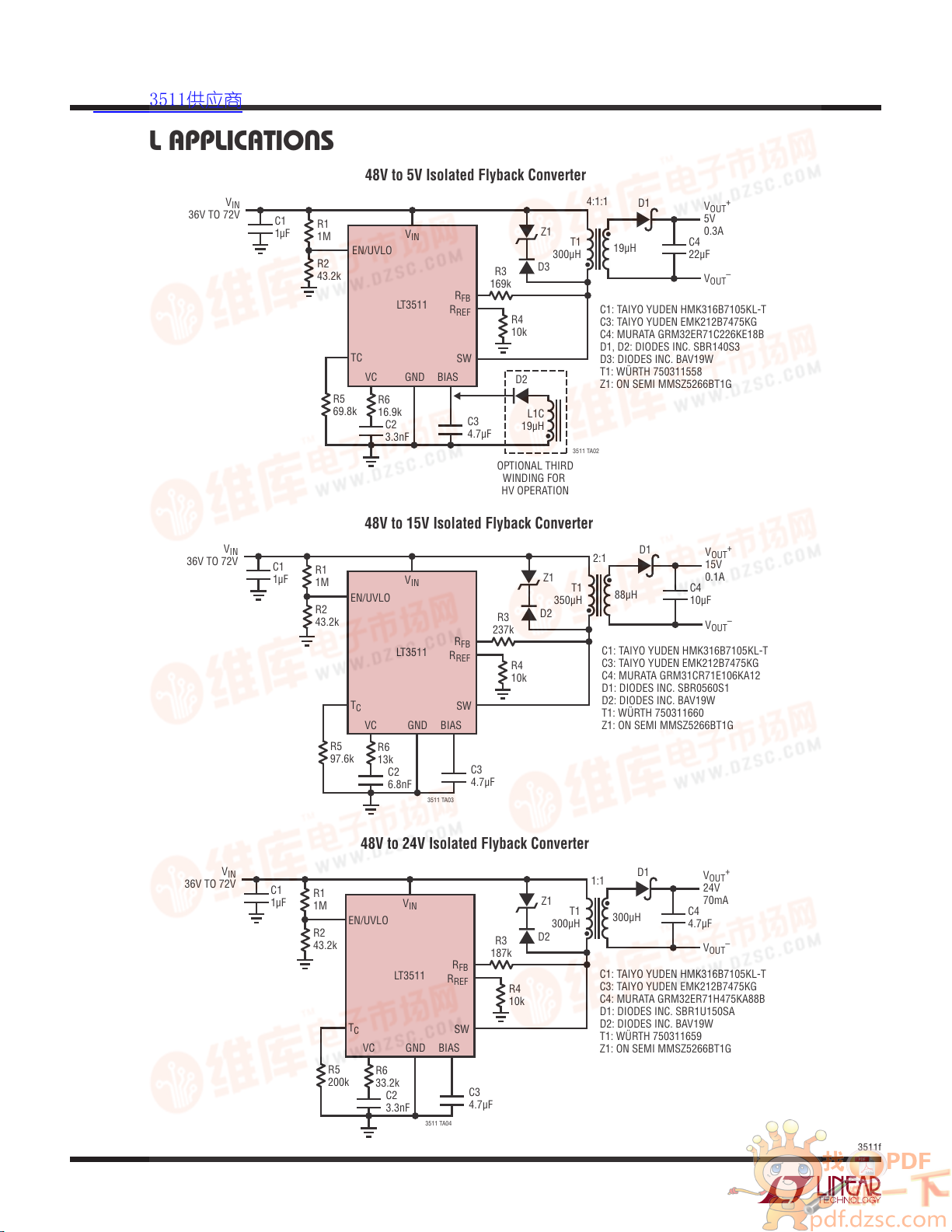
C4: MURATA GRM32ER71H475KA88B
查询LT3511供应商
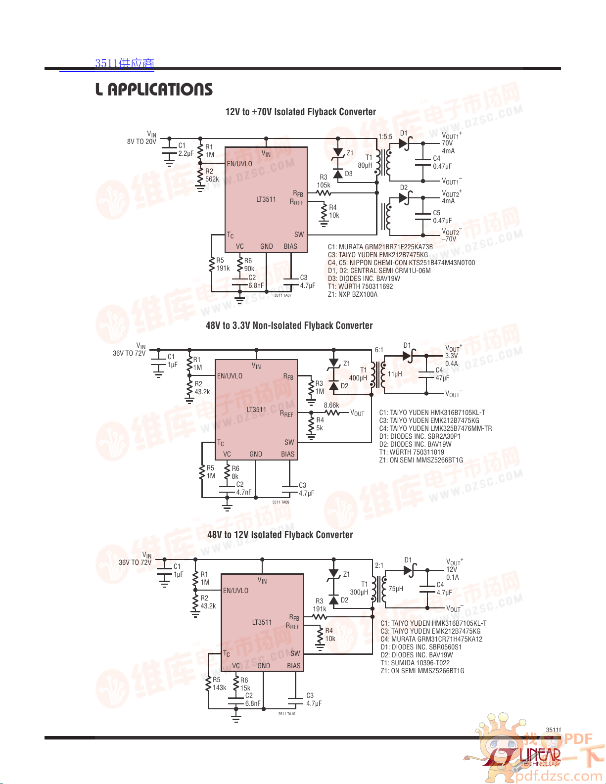
TYPICAL APPLICATIONS
V
IN
36V TO 72V
V
36V TO 72V
C1
R1
µF
1
1M
R2
43.2k
IN
C1
R1
µF
1
1M
R2
43.2k
48V to 5V Isolated Flyback Converter
V
EN/UVLO
TC
R5
69.8k
IN
LT3511
VC GND BIAS
R6
16.9k
C2
3.3nF
R3
169k
R
FB
R
REF
SW
C3
4.7µF
OPTIONAL THIRD
WINDING FOR
HV OPERATION
R4
10k
D2
19µH
48V to 15V Isolated Flyback Converter
V
IN
LT3511
VC GND BIAS
R6
13k
C2
6.8nF
R
3511 TA03
R
REF
SW
R3
237k
FB
R4
10k
C3
4.7µF
R5
97.6k
EN/UVLO
T
C
L1C
4:1:1
Z1
T1
µH
300
D3
3511 TA02
Z1
T1
µH
350
D2
D1
19
µH
C1: TAIYO YUDEN HMK316B7105KL-T
C3: TAIYO YUDEN EMK212B7475KG
C4: MURATA GRM32ER71C226KE18B
D1, D2: DIODES INC. SBR140S3
D3: DIODES INC. BAV19W
T1: WÜRTH 750311558
Z1: ON SEMI MMSZ5266BT1G
D1
2:1
88
µH
C1: TAIYO YUDEN HMK316B7105KL-T
C3: TAIYO YUDEN EMK212B7475KG
C4: MURATA GRM31CR71E106KA12
D1: DIODES INC. SBR0560S1
D2: DIODES INC. BAV19W
T1: WÜRTH 750311660
Z1: ON SEMI MMSZ5266BT1G
+
V
OUT
5V
0.3A
C4
22
µF
–
V
OUT
+
V
OUT
15V
0.1A
C4
10
µF
–
V
OUT
20
V
36V TO 72V
48V to 24V Isolated Flyback Converter
C4
4.7
V
OUT
24V
70mA
µF
V
OUT
+
–
3511f
IN
C1
R1
µF
1
1M
EN/UVLO
R2
43.2k
T
C
R5
200k
V
IN
LT3511
VC GND BIAS
R6
33.2k
C2
3.3nF
3511 TA04
187k
R
FB
R
REF
SW
C3
4.7µF
Z1
T1
µH
300
D2
R3
R4
10k
D1
1:1
300
µH
C1: TAIYO YUDEN HMK316B7105KL-T
C3: TAIYO YUDEN EMK212B7475KG
D1: DIODES INC. SBR1U150SA
D2: DIODES INC. BAV19W
T1: WÜRTH 750311659
Z1: ON SEMI MMSZ5266BT1G
查询LT3511供应商
TYPICAL APPLICATIONS
LT3511
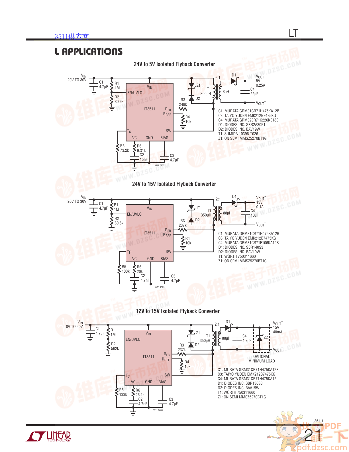
24V to 5V Isolated Flyback Converter
V
20V TO 30V
V
20V TO 30V
IN
C1
4.7
R1
µF
1M
EN/UVLO
R2
80.6k
T
C
R5
73.2k
V
IN
LT3511
VC GND BIAS
R6
9.31k
C2
15nF
R
3511 TA05
249k
R
FB
REF
SW
C3
4.7µF
Z1
T1
µH
300
D2
R3
R4
10k
D1
6:1
8
µH
C1: MURATA GRM31CR71H475KA12B
C3: TAIYO YUDEN EMK212B7475KG
C4: MURATA GRM32ER71C226KE18B
D1: DIODES INC. SBR2A30P1
D2: DIODES INC. BAV19W
T1: SUMIDA 10396-T026
Z1: ON SEMI MMSZ5270BT1G
+
V
OUT
5V
0.25A
C4
µF
22
–
V
OUT
24V to 15V Isolated Flyback Converter
IN
C1
4.7
R1
µF
1M
EN/UVLO
R2
80.6k
T
C
R5
133k
V
IN
LT3511
VC GND BIAS
R6
20k
C2
4.7nF
R
3511 TA06
R
237k
FB
REF
SW
C3
4.7µF
Z1
T1
µH
350
D2
R3
R4
10k
D1
2:1
88
µH
C1: MURATA GRM31CR71H475KA12B
C3: TAIYO YUDEN EMK212B7475KG
C4: MURATA GRM31CR71E106KA12B
D1: DIODES INC. SBR140S3
D2: DIODES INC. BAV19W
T1: WÜRTH 750311660
Z1: ON SEMI MMSZ5270BT1G
+
V
OUT
15V
0.1A
C4
µF
10
–
V
OUT
V
8V TO 20V
12V to 15V Isolated Flyback Converter
IN
C1
4.7
R1
µF
1M
EN/UVLO
R2
562k
T
C
R5
133k
V
IN
LT3511
VC GND BIAS
R6
26.1k
C2
4.7nF
3511 TA08
237k
R
FB
R
REF
SW
C3
4.7µF
Z1
T1
µH
350
D2
R3
R4
10k
D1
2:1
88
C1: MURATA GRM31CR71H475KA12B
C3: TAIYO YUDEN EMK212B7475KG
C4: MURATA GRM31CR71H475KA12
D1: DIODES INC. SBR130S3
D2: DIODES INC. BAV19W
T1: WÜRTH 750311660
Z1: ON SEMI MMSZ5270BT1G
C4
µH
4.7
Z2
µF
OPTIONAL
MINIMUM LOAD
V
OUT
15V
40mA
V
OUT
+
–
3511f
21
LT3511
查询LT3511供应商
TYPICAL APPLICATIONS
12V to ±70V Isolated Flyback Converter
8V TO 20V
V
36V TO 72V
V
IN
C1
2.2
R1
µF
1M
EN/UVLO
R2
562k
T
C
R5
191k
V
IN
LT3511
VC GND BIAS
R6
90k
C2
6.8nF
R
3511 TA07
R
REF
SW
FB
C3
4.7µF
Z1
T1
µH
80
D3
R3
105k
R4
10k
C1: MURATA GRM21BR71E225KA73B
C3: TAIYO YUDEN EMK212B7475KG
C4, C5: NIPPON CHEMI-CON KTS251B474M43N0T00
D1, D2: CENTRAL SEMI CRM1U-06M
D3: DIODES INC. BAV19W
T1: WÜRTH 750311692
Z1: NXP BZX100A
1:5:5
D1
D2
V
70V
4mA
C4
0.47µF
V
V
4mA
C5
0.47µF
V
–70V
OUT1
OUT1
OUT2
OUT2
+
–
+
–
48V to 3.3V Non-Isolated Flyback Converter
IN
C1
R1
µF
1
1M
EN/UVLO
R2
43.2k
T
C
R5
1M
V
IN
R
LT3511
VC GND BIAS
R6
8k
C2
4.7nF
R
3511 TA09
REF
SW
FB
C3
4.7µF
R3
1M
Z1
T1
µH
400
D2
8.66k
V
R4
5k
OUT
D1
6:1
11
µH
C1: TAIYO YUDEN HMK316B7105KL-T
C3: TAIYO YUDEN EMK212B7475KG
C4: TAIYO YUDEN LMK325B7476MM-TR
D1: DIODES INC. SBR2A30P1
D2: DIODES INC. BAV19W
T1: WÜRTH 750311019
Z1: ON SEMI MMSZ5266BT1G
+
V
OUT
3.3V
0.4A
C4
47
µF
–
V
OUT
22
V
36V TO 72V
48V to 12V Isolated Flyback Converter
IN
C1
µF
1
R1
1M
R2
43.2k
R5
143k
EN/UVLO
T
C
V
IN
LT3511
VC GND BIAS
R6
15k
C2
6.8nF
R
3511 TA10
R
REF
SW
191k
FB
C3
4.7µF
Z1
T1
µH
300
D2
R3
R4
10k
D1
2:1
75
µH
C1: TAIYO YUDEN HMK316B7105KL-T
C3: TAIYO YUDEN EMK212B7475KG
C4: MURATA GRM31CR71H475KA12
D1: DIODES INC. SBR0560S1
D2: DIODES INC. BAV19W
T1: SUMIDA 10396-T022
Z1: ON SEMI MMSZ5266BT1G
C4
4.7
V
12V
0.1A
µF
V
OUT
OUT
+
–
3511f

1.0
查询LT3511供应商
PACKAGE DESCRIPTION
LT3511
MS Package
Varitation: MS16 (12)
16-Lead Plastic MSOP with 4 Pins Removed
(Reference LTC DWG # 05-08-1847 Rev A)
(.0197)
0° – 6° TYP
0.53 ± 0.152
(.021 ± .006)
0.889 ± 0.127
(.035 ± .005)
3.20 – 3.45
(.126 – .136)
0.50
BSC
SEATING
PLANE
4.90 ± 0.152
(.193 ± .006)
(.043)
0.17 –0.27
(.007 – .011)
TYP
1.10
MAX
4.039 ± 0.102
(.159 ± .004)
(NOTE 3)
16 14 12 1110
1 3 5 6 7 8
1.0
(.0394)
BSC
0.50
(.0197)
BSC
(.0394)
BSC
5.23
(.206)
MIN
0.305 ± 0.038
(.0120 ± .0015)
TYP
RECOMMENDED SOLDER PAD LAYOUT
0.254
(.010)
GAUGE PLANE
0.18
(.007)
NOTE:
1. DIMENSIONS IN MILLIMETER/(INCH)
2. DRAWING NOT TO SCALE
3. DIMENSION DOES NOT INCLUDE MOLD FLASH, PROTRUSIONS OR GATE BURRS.
MOLD FLASH, PROTRUSIONS OR GATE BURRS SHALL NOT EXCEED 0.152mm (.006") PER SIDE
4. DIMENSION DOES NOT INCLUDE INTERLEAD FLASH OR PROTRUSIONS.
INTERLEAD FLASH OR PROTRUSIONS SHALL NOT EXCEED 0.152mm (.006") PER SIDE
5. LEAD COPLANARITY (BOTTOM OF LEADS AFTER FORMING) SHALL BE 0.102mm (.004") MAX
DETAIL “A”
DETAIL “A”
0.280 ± 0.076
(.011 ± .003)
9
3.00 ± 0.102
(.118 ± .004)
(NOTE 4)
(.034)
MSOP (MS12) 0510 REV A
REF
0.86
REF
0.1016 ± 0.0508
(.004 ± .002)
Information furnished by Linear Technology Corporation is believed to be accurate and reliable.
However, no responsibility is assumed for its use. Linear Technology Corporation makes no representation that the interconnection of its circuits as described herein will not infringe on existing patent rights.
3511f
23
LT3511
查询LT3511供应商
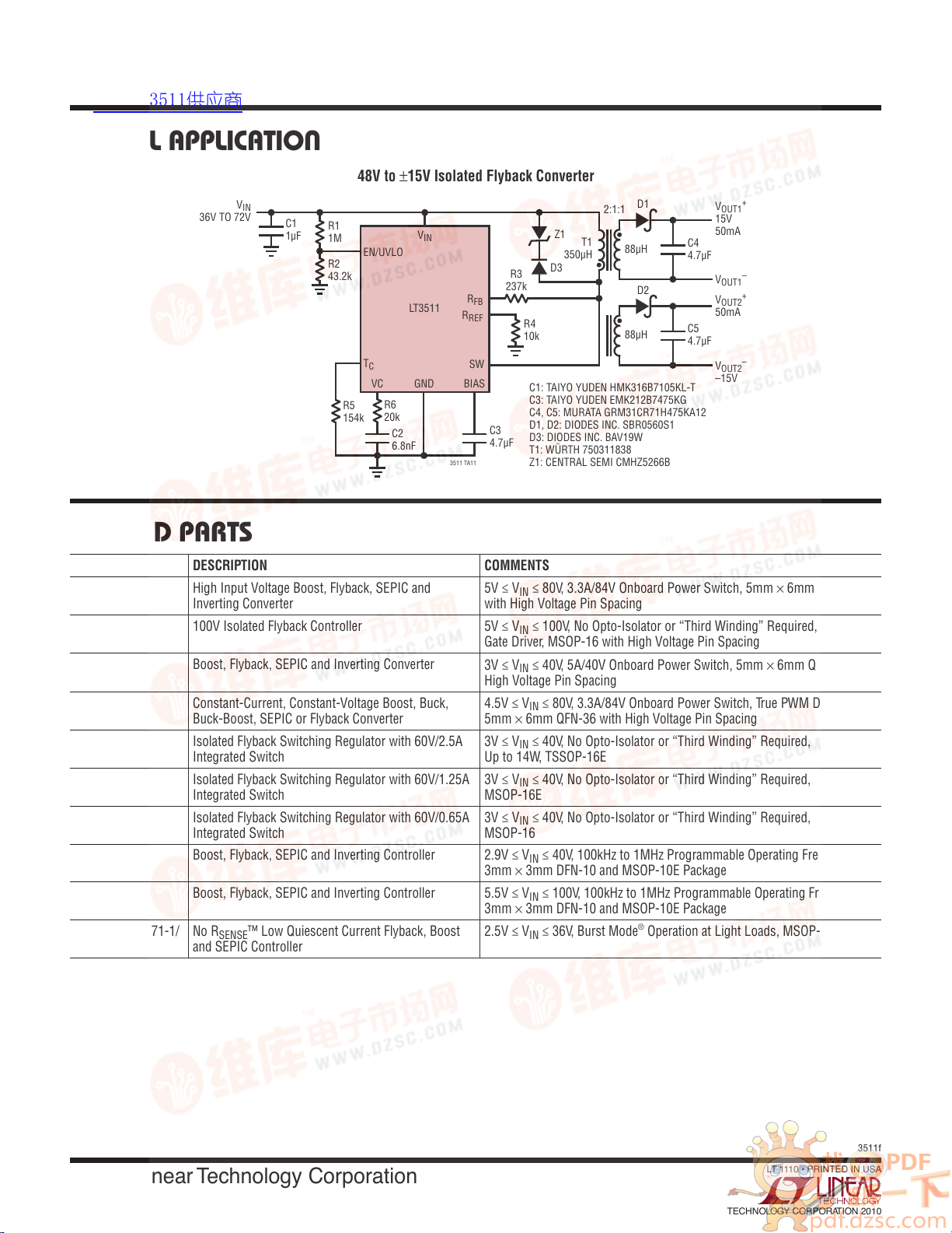
TYPICAL APPLICATION
V
IN
36V TO 72V
C1
µF
1
RELATED PARTS
48V to ±15V Isolated Flyback Converter
R1
1M
R2
43.2k
R5
154k
EN/UVLO
T
C
V
IN
LT3511
VC GND BIAS
R6
20k
C2
6.8nF
R
3511 TA11
R
REF
SW
R3
237k
FB
R4
10k
C1: TAIYO YUDEN HMK316B7105KL-T
C3: TAIYO YUDEN EMK212B7475KG
C4, C5: MURATA GRM31CR71H475KA12
D1, D2: DIODES INC. SBR0560S1
C3
D3: DIODES INC. BAV19W
4.7µF
T1: WÜRTH 750311838
Z1: CENTRAL SEMI CMHZ5266B
D1
2:1:1
Z1
T1
88
µH
350
D3
µH
D2
88µH
C4
4.7
C5
4.7
+
V
OUT1
15V
50mA
µF
–
V
OUT1
+
V
OUT2
50mA
µF
–
V
OUT2
–15V
PART NUMBER DESCRIPTION COMMENTS
LT3958 High Input Voltage Boost, Flyback, SEPIC and
Inverting Converter
LT3748 100V Isolated Flyback Controller 5V ≤ V
≤ 80V, 3.3A/84V Onboard Power Switch, 5mm × 6mm QFN-36
5V ≤ V
IN
with High Voltage Pin Spacing
≤ 100V, No Opto-Isolator or “Third Winding” Required, Onboard
IN
Gate Driver, MSOP-16 with High Voltage Pin Spacing
LT3957 Boost, Flyback, SEPIC and Inverting Converter
3V ≤ VIN ≤ 40V, 5A/40V Onboard Power Switch, 5mm × 6mm QFN-36 with
High Voltage Pin Spacing
LT3956 Constant-Current, Constant-Voltage Boost, Buck,
Buck-Boost, SEPIC or Flyback Converter
LT3575 Isolated Flyback Switching Regulator with 60V/2.5A
Integrated Switch
LT3573 Isolated Flyback Switching Regulator with 60V/1.25A
Integrated Switch
LT3574 Isolated Flyback Switching Regulator with 60V/0.65A
Integrated Switch
4.5V ≤ V
5mm × 6mm QFN-36 with High Voltage Pin Spacing
3V ≤ V
Up to 14W, TSSOP-16E
3V ≤ V
MSOP-16E
3V ≤ V
MSOP-16
LT3757 Boost, Flyback, SEPIC and Inverting Controller 2.9V ≤ V
≤ 80V, 3.3A/84V Onboard Power Switch, True PWM Dimming,
IN
≤ 40V, No Opto-Isolator or “Third Winding” Required,
IN
≤ 40V, No Opto-Isolator or “Third Winding” Required, Up to 7W,
IN
≤ 40V, No Opto-Isolator or “Third Winding” Required, Up to 3W,
IN
≤ 40V, 100kHz to 1MHz Programmable Operating Frequency,
IN
3mm × 3mm DFN-10 and MSOP-10E Package
LT3758 Boost, Flyback, SEPIC and Inverting Controller 5.5V ≤ V
≤ 100V, 100kHz to 1MHz Programmable Operating Frequency,
IN
3mm × 3mm DFN-10 and MSOP-10E Package
LTC1871/LTC1871-1/
LTC1871-7
No R
™ Low Quiescent Current Flyback, Boost
SENSE
and SEPIC Controller
2.5V ≤ VIN ≤ 36V, Burst Mode® Operation at Light Loads, MSOP-10
24
Linear Technology Corporation
1630 McCarthy Blvd., Milpitas, CA 95035-7417
(408) 432-1900 ● FAX: (408) 434-0507
●
www.linear.com
3511f
LT 1110 • PRINTED IN USA
LINEAR TECHNOLOGY CORPORATION 2010
 Loading...