

LT3510
Monolithic Dual Tracking
2A Step-Down Switching
Regulator
FEATURES
n
Wide Input Range: 3.1V to 25V
n
Two Switching Regulators with 2A Output Capability
n
Independent Supply to Each Regulator
n
Adjustable/Synchronizable Fixed Frequency
Operation from 250kHz to 1.5MHz
n
Antiphase Switching
n
Outputs Can be Paralleled
n
Independent, Sequential, Ratiometric or Absolute
Tracking Between Outputs
n
Independent Soft-Start and Power Good Pins
n
Enhanced Short-Circuit Protection
n
Low Dropout: 95% Maximum Duty Cycle
n
Low Shutdown Current: <10μA
n
20-Lead TSSOP Package with Exposed Leadframe
APPLICATIONS
n
DSP Power Supplies
n
Disc Drives
n
DSL/Cable Modems
n
Wall Transformer Regulation
n
Distributed Power Regulation
n
PCI Cards
, LT, LTC, and LTM are registered trademarks of Linear Technology Corporation.
All other trademarks are the property of their respective owners.
DESCRIPTION
The LT®3510 is a dual current mode PWM step-down
DC/DC converter with two internal 2.5A switches. Independent input voltage, feedback, soft-start and power
good pins for each channel simplify complex power
supply tracking/sequencing requirements.
Both converters are synchronized to either a common
external clock input or a resistor programmable fi xed
250kHz to 1.5MHz internal oscillator. At all frequencies, a
180° phase relationship between channels is maintained,
reducing voltage ripple and component size. Programmable
frequency allows for optimization between effi ciency and
external component size.
Minimum input-to-output voltage ratios are improved
by allowing the switch to stay on through multiple clock
cycles, only switching off when the boost capacitor needs
recharging, resulting in ~95% maximum duty cycle.
Each output can be independently disabled using its own
soft-start pin, or by using the SHDN pin the entire part can
be placed in a low quiescent current shutdown mode.
The LT3510 is available in a 20-lead TSSOP package with
exposed leadframe for low thermal resistance.
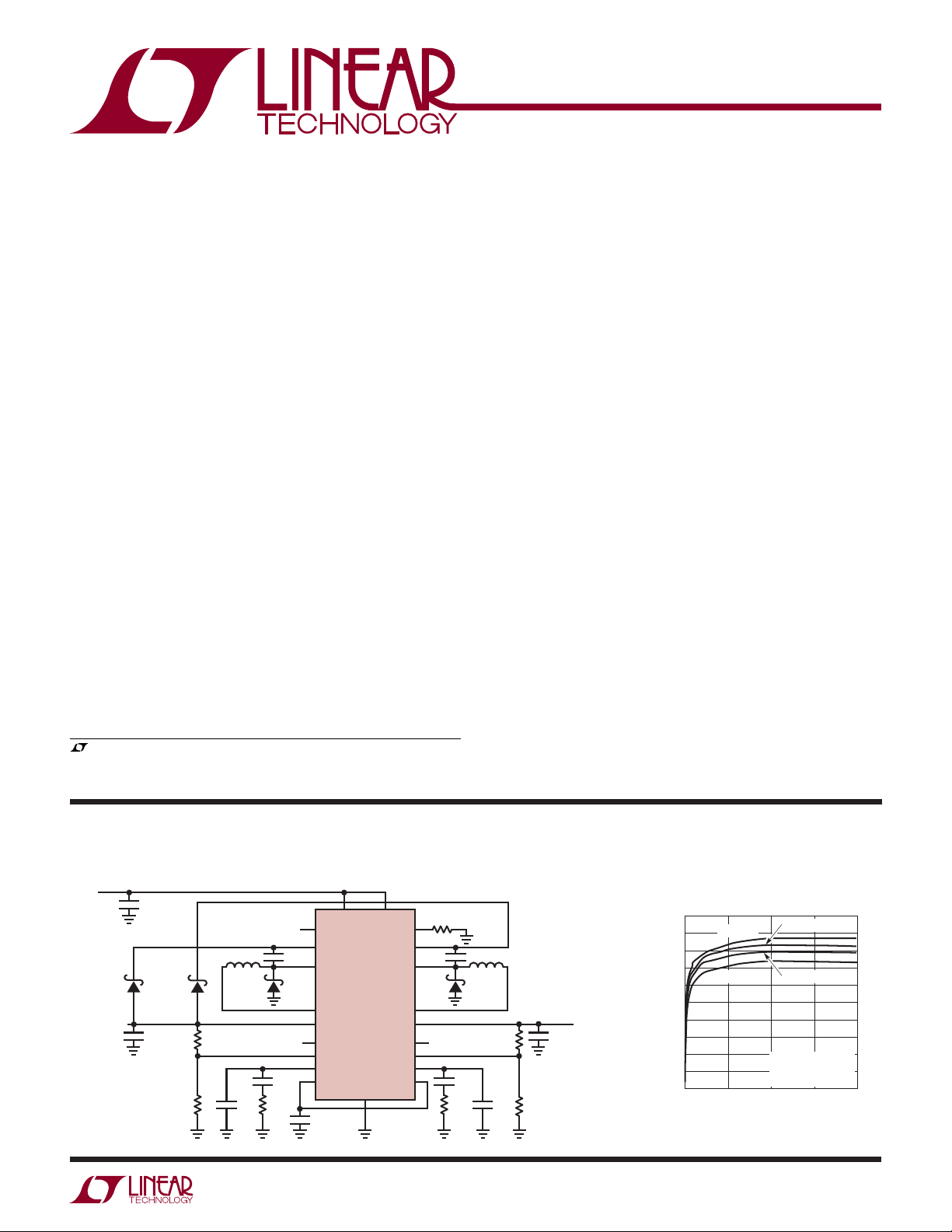
TYPICAL APPLICATION
3.3V and 1.8V Dual 2A Step-Down Converter with Output Tracking
V
IN
12V
4.7μF
PMEG4005
V
OUT1
3.3V
2A
4.7μH
PMEG4005
47μF 100μF
24.9k
8.06k
0.47μF
B360A B360A
470pF
40.2k
10pF 47pF
SHDN
BST1
SW1
IND1
V
OUT1
PG1
FB1
V
C1
SS/TRACK1
0.1μF
Effi ciency
V
IN1
LT3510
GND
V
IN2
R
/SYNC
T
BST2
SW2
IND2
V
OUT2
PG2
FB2
V
SS/TRACK2
61.9k
470pF
40.2k
3.3μH
10k
8.06k
3510 TA01a
V
1.8V
2A
OUT2
0.47μF
C2
100
90
80
70
60
50
40
EFFICIENCY (%)
30
20
10
0
0
V
= 5V
OUT
V
= 1.8V
OUT
0.5
LOAD CURRENT (A)
V
= 3.3V
OUT
V
= 2.5V
OUT
VIN = 12V
= 0A
I
OUT2
FREQUENCY = 500kHz
1.5
1
3510 TA01b
2
3510fc
1

LT3510
ABSOLUTE MAXIMUM RATINGS
PIN CONFIGURATION
(Note 1)
V
, SHDN, PG1/2 ...................................... 25V/–0.3V
IN1/2
SW1/2 .................................................................... V
IN1/2
BST1/2 ........................................................... 35V/–0.3V
BST1/2 Pins Above SW1/2 ........................................25V
IND1/2 .....................................................................±4A
V
FB1/2, SS1/2, R
V
........................................................ V
OUT1/2
/SYNC ............................................5.5V
T
......................................................................±1mA
C1/2
IN1/2
/–0.3V
Operating Junction Temperature Range
LT3510EFE (Notes 2, 8) ..................... –40°C to 125°C
LT3510IFE (Notes 2, 8) ...................... –40°C to 125°C
Storage Temperature Range ...................–65°C to 150°C
Lead Temperature (Soldering, 10 sec) ..................300°C
V
IN1
SW1
IND1
V
OUT1
PG1
PG2
V
OUT2
IND2
SW2
V
IN2
T
= 125°C, θJA = 45°C/W, θ
JMAX
EXPOSED PAD (PIN 21) IS GND, MUST BE SOLDERED TO PCB
TOP VIEW
1
2
3
4
5
6
7
8
9
10
FE PACKAGE
20-LEAD PLASTIC TSSOP
20
19
18
17
16
21
15
14
13
12
11
JC(PAD)
BST1
SS/TRACK1
V
C1
FB1
R
/SYNC
T
SHDN
FB2
V
C2
SS/TRACK2
BST2
= 10°C/W
ORDER INFORMATION
LEAD FREE FINISH TAPE AND REEL PART MARKING* PACKAGE DESCRIPTION TEMPERATURE RANGE
LT3510EFE#PBF LT3510EFE#TRPBF LT3510FE 20-Lead TSSOP –40°C to 125°C
LT3510IFE#PBF LT3510IFE#TRPBF LT3510FE 20-Lead TSSOP –40°C to 125°C
LEAD BASED FINISH TAPE AND REEL PART MARKING* PACKAGE DESCRIPTION TEMPERATURE RANGE
LT3510EFE LT3510EFE#TR LT3510FE 20-Lead TSSOP –40°C to 125°C
LT3510IFE LT3510IFE#TR LT3510FE 20-Lead TSSOP –40°C to 125°C
Consult LTC Marketing for parts specifi ed with wider operating temperature ranges. *The temperature grade is identifi ed by a label on the shipping container.
For more information on lead free part marking, go to:
For more information on tape and reel specifi cations, go to:
http://www.linear.com/leadfree/
http://www.linear.com/tapeandreel/
The
ELECTRICAL CHARACTERISTICS
temperature range, otherwise specifi cations are at TJ = 25°C. V
l denotes the specifi cations which apply over the full operating
VIN1/2
= 15V, V
BST1/2
= open, V
RT/SYNC
= 2V, V
VOUT1/2
= open,
unless otherwise specifi ed.
PARAMETER CONDITIONS MIN TYP MAX UNITS
SHDN Threshold V
SHDN Input Current V
Minimum Input Voltage Ch 1 (Note 3) V
Minimum Input Voltage Ch 2 V
Supply Shutdown Current Ch 1 V
Supply Shutdown Current Ch 2 V
Supply Quiescent Current Ch 1 V
Supply Quiescent Current Ch 2 V
Feedback Voltage Ch 1/2 V
= 0V, RT/SYNC = 133k
OUT1/2
= 1.375V
SHDN
V
= 1.225V
SHDN
= 0V, V
FB1/2
= 0V, V
FB1/2
= 0V
SHDN
= 0V 0 5 μA
SHDN
= 0.9V 3.5 5 mA
FB1/2
= 0.9V 200 500 μA
FB1/2
= 1V
VC1/2
VOUT1/2
VOUT1/2
= 0V, V
= 0V, V
= 0V, RT/SYNC = 133k 2.8 3 V
IND1/2
= 0V 2.8 3 V
IND1/2
l
1.23 1.28 1.37 V
7
2
l
l
0.784 0.8 0.816 V
10
13
3
930 μA
5
μA
3510fc
μA
2
LT3510
ELECTRICAL CHARACTERISTICS
The l denotes the specifi cations which apply over the full operating
temperature range, otherwise specifi cations are at T
unless otherwise specifi ed.
PARAMETER CONDITIONS MIN TYP MAX UNITS
Feedback Voltage Line Regulation V
Feedback Voltage Offset Ch 1 to Ch 2 V
Feedback Bias Current Ch 1/2 V
Error Amplifi er g
Ch 1/2 V
m
Error Amplifi er Gain Ch 1/2 1000 V/V
Error Amplifi er to Switch Gain Ch 1/2 2.2 A/V
Error Amplifi er Source Current Ch 1/2 V
Error Amplifi er Sink Current Ch 1/2 V
Error Amplifi er High Clamp Ch 1/2 V
Error Amplifi er Switching Threshold Ch 1/2 V
Soft-Start Source Current Ch 1/2 V
Soft-Start V
Ch 1/2 V
OH
Soft-Start Sink Current Ch 1/2 V
Soft-Start V
Ch 1/2 V
OL
Soft-Start to Feedback Offset Ch 1/2 V
Soft-Start Sink Current Ch 1/2 POR V
Soft-Start POR Threshold Ch 1/2 V
Soft-Start Switching Threshold Ch 1/2 V
Power Good Leakage Ch 1/2 V
Power Good Threshold Ch 1/2 V
Power Good Hysteresis Ch 1/2 V
Power Good Sink Current Ch 1/2 V
Power Good Shutdown Sink Current Ch 1/2 V
/SYNC Reference Voltage V
R
T
Switching Frequency R
Switching Phase Angle Ch A to Ch B R
Minimum Boost for 100% Duty Cycle Ch 1/2 V
SYNC Frequency Range V
SYNC Switching Phase Angle Ch A to Ch B SYNC = 250kHz, V
IND + V
IND to V
Current Ch 1/2 V
OUT
Maximum Current Ch 1/2 V
OUT
Switch Leakage Current Ch 1/2 V
Switch Saturation Voltage Ch 1/2 I
Boost Current Ch 1/2 I
Minimum Boost Voltage Ch 1/2 I
Note 1: Stresses beyond those listed under Absolute Maximum Ratings
may cause permanent damage to the device. Exposure to any Absolute
Maximum Rating condition for extended periods may affect device
reliability and lifetime.
VIN1/2
VC1/2
FB1/2
VC1/2
FB1/2
FB1/2
FB1/2
OUT1/2
FB1/2
FB1/2
FB1/2
FB1/2
VC1/2
SS1/2
FB1/2
FB1/2
FB1/2
FB1/2
FB1/2
FB1/2
VIN1/2
FB1/2
T
R
T
T
FB1/2
BST1/2
VOUT1/2
V
VOUT1/2
VOUT1/2
V
VOUT1/2
SW1/2
SW1/2
SW1/2
SW1/2
= 25°C. V
J
= 3V to 25V
= 1V
= 0.8V, V
= 1V, I
= 0.6V, V
= 1V, V
VC1/2
VC1/2
VC1/2
VC1/2
= ±5μA
= 1V 15 20 30 μA
VIN1/2
= 1V
= 15V, V
BST1/2
= open, V
RT/SYNC
l
l
l
l
= 2V, V
VOUT1/2
= open,
–1 0 1 %
–16 0 16 mV
–200 75 200 nA
150 275 450 μmho
= 1V 10 15 25 μA
= 0.7V 1.75 2.0 2.25 V
= 5V, RT/SYNC = 133k 0.5 0.7 1.0 V
= 0.6V, V
SS1/2
= 0.4V
l
2.5 3.25 4 μA
= 0.9V 1.9 2 2.4 V
= 0.6V, V
= 1V 200 600 1000 μA
SS1/2
= 0V 50 80 125 mV
= 1V, V
SS1/2
= 0.4V
l
–16 0 16 mV
= 0.4V (Note 4), VVC = 1V 0.5 1.5 2 mA
= 0V (Note 4) 55 80 105 mV
= 0V 30 50 70 mV
= 0.9V, V
Rising, PG1/2 = 20k to 5V
PG1/2
= 25V, V
VIN1/2
= 25V, V
= 5V 0 1 μA
OUT
l
87 90 93 %
Falling, PG1/2 = 20k to 5V 20 30 50 mV
= 0.65V, V
= 2V, V
= 0.9V, I
/SYNC = 133k, V
/SYNC = 15.4k, V
/SYNC = 133k, V
= 0.7V, I
= 0.4V 400 800 1200 μA
PG1/2
= 0V, V
FB1/2
= –40μA 0.93 0.975 1 V
RT/SYNC
FB1/2
FB1/2
FB1/2
= –35μA (Note 5), V
RT/SYNC
= 0.4V 10 50 100 μA
PG1/2
= 0.6V, V
= 0.6V, V
= 0.6V, V
= VSW + 3V
BST1/2
= VSW + 3V
BST1/2
= VSW + 3V 120 180 210 Deg
BST1/2
= 0V 1.7 2 V
OUT
200
1.2
250
1.5
300
1.8
= VSW + 3V 250 1500 kHz
= VSW + 3V 120 180 210 Deg
BST1/2
= 0V, V
= 5V
= 0.5V (Note 6), V
= 5V (Note 6), RT/SYNC = 133k, V
= 0V, V
= 2A, V
= 2A, V
= 2A, V
= 0.9V
FB1/2
VIN1/2 = 25V
= 20V, V
BST1/2
= 20V, V
BST1/2
= 20V, V
BST1/2
40 70
100
0
= 0.7V, V
FB1/2
= 0.7V
FB1/2
= 0.7V 25 50 100 mA
FB1/2
= 0.7V (Note 7) 1.4 2.5 V
FB1/2
BST1/2
BST1/2
= 20V
= 20V
2.25
2.5
l
l
2.8
2.8
050 μA
250 400 mV
1
4
4
Note 2: The LT3510EFE is guaranteed to meet performance specifi cations
from 0°C to 125°C junction temperature. Specifi cations over the –40°C
to 125°C operating junction temperature range are assured by design,
characterization and correlation with statistical process controls. The
kHz
MHz
μA
μA
A
A
3510fc
3
LT3510
ELECTRICAL CHARACTERISTICS
LT3510IFE is guaranteed and tested over the full –40°C to 125°C operating
junction temperature range.
Note 3: Minimum input voltage is defi ned as the voltage where internal
bias lines are regulated so that the reference voltage and oscillator remain
constant. Actual minimum input voltage to maintain a regulated output
will depend upon output voltage and load current. See Applications
Information.
Note 4: An internal power-on reset (POR) latch is set on the positive
transition of the SHDN pin through its threshold. The output of the latch
activates current sources on each SS pin which typically sink 1.5mA,
discharging the SS capacitor. The latch is reset when both SS pins are
driven below the soft-start POR threshold or the SHDN pin is taken below
its threshold.
Note 5: To enhance dropout operation, the output switch will be turned off
for the minimum off time only when the voltage across the boost capacitor
drops below the minimum boost for 100% duty cycle threshold.
Note 6: The IND to V
current fl owing from the IND pin to the V
latch when the V
Note 7: This is the minimum voltage across the boost capacitor needed to
guarantee full saturation of the internal power switch.
Note 8: This IC includes overtemperature protection that is intended
to protect the device during momentary overload conditions. Junction
temperature will exceed 125°C when overtemperature protection is active.
Continuous operation above the specifi ed maximum operating junction
temperature may impair device reliability.
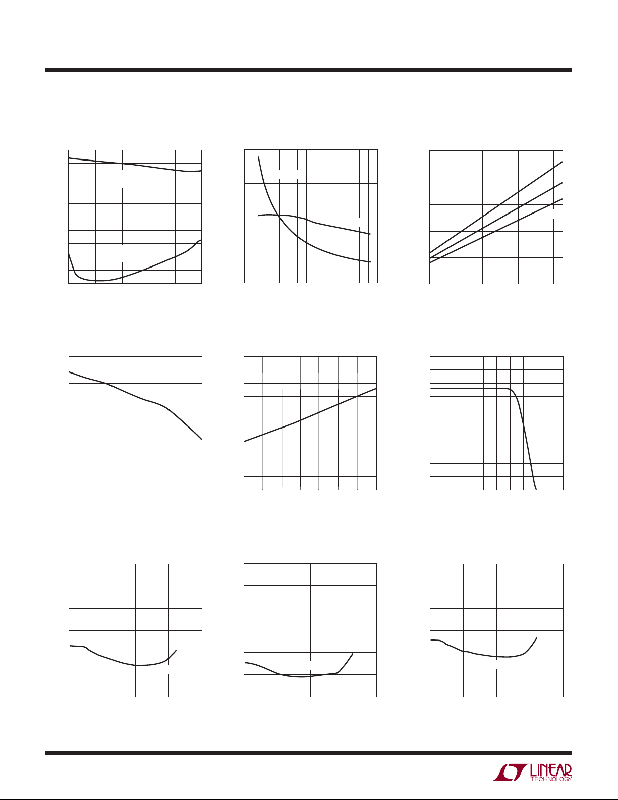
TYPICAL PERFORMANCE CHARACTERISTICS
Feedback Voltage vs Temperature RT/SYNC Voltage vs Temperature
0.816
0.811
0.806
0.801
VOLTAGE (V)
0.796
1.05
1.03
1.01
0.99
VOLTAGE (V)
maximum current is defi ned as the value of
OUT
pin is at its high clamp.
C
pin which resets the switch
OUT
Shutdown Threshold and Minimum
Input Voltage vs Temperature
3.0
2.5
2.0
1.5
VOLTAGE (V)
1.0
MINIMUM INPUT
VOLTAGE
SHUTDOWN
THRESHOLD
VOLTAGE
0.791
0.786
–50
–25 0
TEMPERATURE (°C)
50 100 125
25 75
Shutdown Quiescent Current
vs Temperature
16
14
12
10
CURRENT (μA)
V
VIN1
8
6
4
2
0
–25 0 50
–50
25
TEMPERATURE (°C)
3510 G02
V
VIN2
75 100 125
3510 G05
0.97
0.95
–50 –25
25
0
TEMPERATURE (°C)
Soft-Start Source Current
vs Temperature
4.0
3.8
3.6
3.4
3.2
3.0
2.8
CURRENT (μA)
2.6
2.4
2.2
2.0
–50
–25
25
0
TEMPERATURE (°C)
0.5
0
–50
50
75
100
125
3510 G03
–25 0
IND to V
TEMPERATURE (°C)
OUT
50 100 125
25 75
3510 G04
Maximum Current vs
Temperature
4.0
3.8
3.6
3.4
3.2
3.0
2.8
CURRENT (A)
2.6
2.4
2.2
2.0
–30 10
50
75
100
125
3510 G07
–50
V
OUT
V
OUT
–10
30
TEMPERATURE (°C)
= 5V
= 0V
50
90
110
70
3510 G30
3510fc
4
TYPICAL PERFORMANCE CHARACTERISTICS
LT3510
Soft-Start to Feedback Offset
Voltage vs Temperature
4
3
2
1
0
–1
VOLTAGE (mV)
–2
–3
–4
–25 0 50
–50
25
TEMPERATURE (°C)
Power Good Sink Current
vs Temperature
1000
950
900
850
800
750
700
CURRENT (μA)
650
600
550
500
–50
0
–25
TEMPERATURE (°C)
50
25
75 100 125
3510 G08
100
125
3510 G11
75
Switching Threshold Voltage
V
C
vs Temperature
1000
900
800
700
VOLTAGE (V)
600
500
400
–50
–25 0
V
OUT
V
= 0V
OUT
25 75
TEMPERATURE (°C)
Minimum Switching Times
vs Temperature
250
230
210
MINIMUM ON TIME
190
170
150
TIME (ns)
130
110
90
70
50
–50
–25
MINIMUM OFF TIME
25
0
TEMPERATURE (°C)
= 5V
50 100 125
3510 G09
50
75
100
3510 G12
125
Power Good Threshold Voltage
vs Temperature
800
780
760
740
720
700
680
VOLTAGE (V)
660
640
620
600
–50
–25
RISING
FALLING
50
25
0
TEMPERATURE (°C)
75
Switching Frequency and Channel
Phase vs Temperature
300
RT/SYNC = 133k
290
280
PHASE
270
260
250
FREQUENCY
240
FREQUENCY (kHz)
230
220
210
200
–50
–25
0
TEMPERATURE (°C)
50
25
75
100
100
3510 G10
3510 G13
125
125
200
190
180
170
PHASE (DEG)
160
150
140
130
120
110
100
Switching Frequency and Channel
Phase vs Temperature
1650
RRT/SYNC = 15.4k
1600
1550
1500
1450
FREQUENCY (kHz)
1400
1350
–50
PHASE
FREQUENCY
–25 0
50 100 125
25 75
TEMPERATURE (°C)
3510 G14
200
195
190
185
PHASE (DEG)
180
175
170
165
160
155
150
Synchronization Clock Frequency
Range vs Temperature
2500
2000
MAXIMUM
1500
1000
FREQUENCY (kHz)
500
0
–50 –25
SYNCHRONIZATION
FREQUENCY
MINIMUM
SYNCHRONIZATION
FREQUENCY
50
25
0
TEMPERATURE (°C)
Channel Phase vs Temperature
with External Synchronization
188
186
164
182
180
178
176
PHASE (DEG)
174
172
170
168
100
125
3510 G15
75
–50
SYNCHRONIZATION
FREQUENCY = 250kHz
SYNCHRONIZATION
FREQUENCY = 1500kHz
0
–25
TEMPERATURE (°C)
50
25
75
100
125
3510 G16
3510fc
5
LT3510
TYPICAL PERFORMANCE CHARACTERISTICS
External Sync Duty Cycle Range
vs External Sync Frequency
100
90
80
70
60
50
40
DUTY CYCLE (%)
30
20
10
0
250
MAXIMUM CLOCK
DUTY CYCLE
MINIMUM CLOCK
DUTY CYCLE
500
750
FREQUENCY (kHz)
1000
Minimum Boost Voltage
vs Temperature
2.5
2.0
1.5
1.0
VOLTAGE (V)
0.5
0
–50 –25
0
TEMPERATURE (°C)
50
25
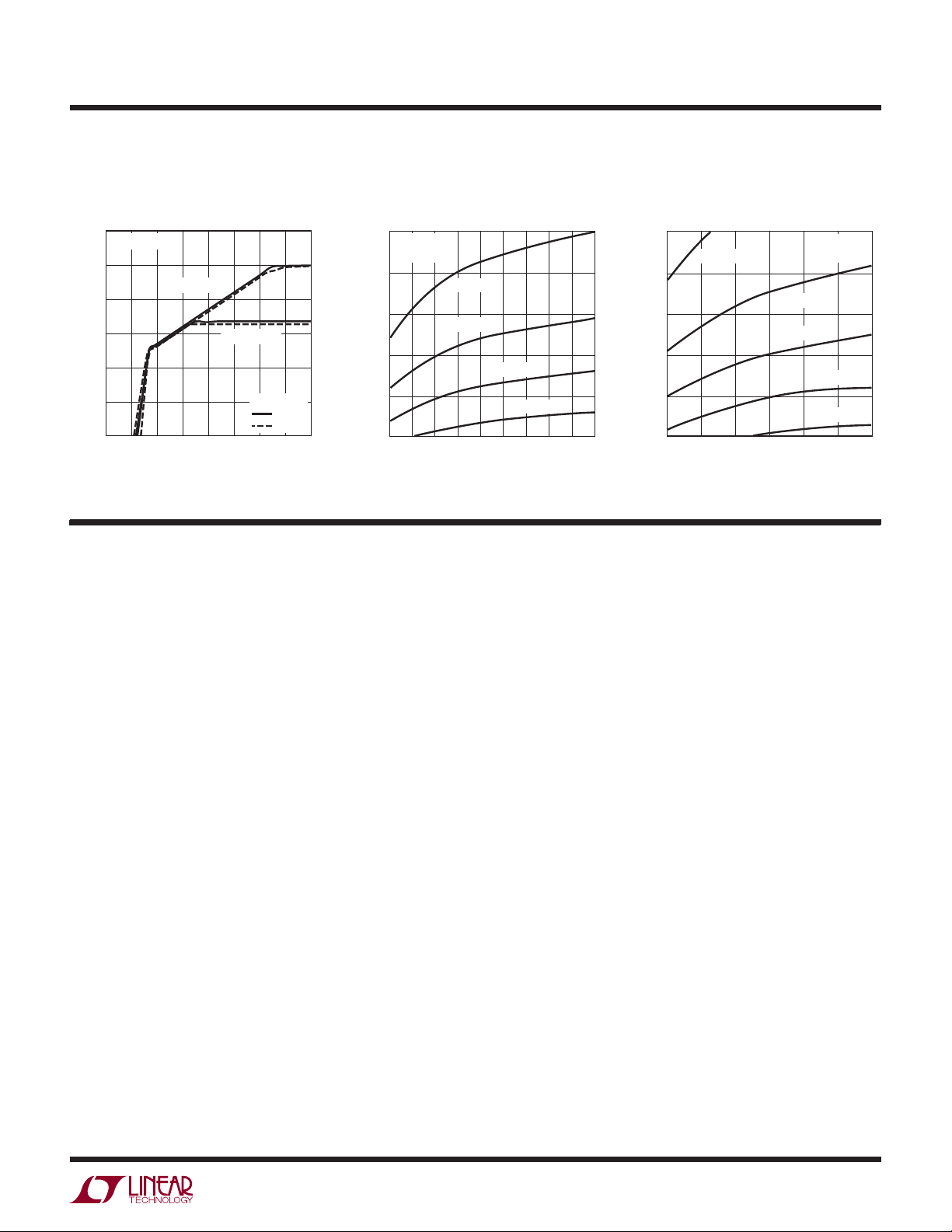
Frequency and Phase vs RT/SYNC
Pin Resistance
1250
3510 G17
1500
1600
1400
1200
1000
800
600
FREQUENCY (kHz)
400
200
100
FREQUENCY
0 20 40 60 80 100 120 140
RESISTANCE (kΩ)
V
+ IND Current
OUT
PHASE
3510 G18
190
185
180
PHASE (DEG)
175
170
165
160
155
150
vs Temperature
100
95
90
85
80
75
70
CURRENT (μA)
65
60
55
100
125
3510 G21
75
50
–50
–25
0
TEMPERATURE (°C)
50
25
75
100
125
3510 G22
Switch Saturation Voltage
vs Switch Current
250
200
150
100
VOLTAGE (mV)
50
0
0.5
0.7 0.9
V
OUT
vs V
100
90
80
70
60
50
40
CURRENT (μA)
30
20
10
0
0
OUT
1.1 1.5
CURRENT (A)
+ IND Current
Voltage
0.40.2
0.80.6
VOLTAGE (V)
1.3
1.2 1.4 1.8
1.0
125°C
25°C
–50°C
1.7 1.9
1.6
3510 G19
2.0
3510 G23
Minimum Input Voltage
vs Load Current
5.0
V
= 2.5V
OUT
4.5
4.0
3.5
VOLTAGE (V)
3.0
2.5
2.0
1
10 100 1000 10000
6
CURRENT (mA)
RUNNING
3510 G24
Minimum Input Voltage
vs Load Current
6.0
V
= 3.3V
OUT
5.5
5.0
4.5
VOLTAGE (V)
4.0
3.5
3.0
1
10 100 1000 10000
CURRENT (mA)
RUNNING
3510 G25
Minimum Input Voltage
vs Load Current
7.5
V
= 5V
OUT
7.0
6.5
6.0
VOLTAGE (V)
5.5
5.0
4.5
1
10 100 1000 10000
CURRENT (mA)
RUNNING
3510 G26
3510fc
TYPICAL PERFORMANCE CHARACTERISTICS
LT3510
Inductor Value vs Frequency for
Dropout Operation
6
LOAD = 1A
5
4
3
2
OUTPUT VOLTAGE (V)
1
0
2
34
2.5 3.5
V
= 5V
OUT
V
OUT
INPUT VOLTAGE (V)
4.5
= 3.3V
FREQUENCY
1.5MHz
250kHz
5
5.5
6
3510 G27
2A Maximum Load Current
1500
V
= 3.3V
OUT
= 1A
I
RIPPLE
1250
1000
750
FREQUENCY (kHz)
500
250
7
L = 2.2μH
L = 3.3μH
913
11
INPUT VOLTAGE (V)
PIN FUNCTIONS
V
(Pin 1): The V
IN1
circuitry for both channels and is monitored by the
undervoltage lockout comparator. The V
connected to the collector of channel 1’s on-chip power
NPN switch. The V
be decoupled to ground close to the pin of the device.
SW1/SW2 (Pins 2, 9): The SW pin is the emitter of the onchip power NPN. At switch off, the inductor will drive this
pin below ground with a high dV/dt. An external Schottky
catch diode to ground, close to the SW pin and respective
decoupling capacitor’s ground, must be used to prevent
V
IN
this pin from excessive negative voltages.
IND1/IND2 (Pins 3, 8): The IND pin is the input to the
on-chip sense resistor that measures current fl owing in
the inductor. When the current in the resistor exceeds
the current dictated by the V
reset, disabling the output switch. Bias current fl ows out
of the IND pin when IND is less than 1.6V.
pin powers the internal control
IN1
pin is also
IN1
pin has high dI/dt edges and must
IN1
pin, the SW latch is held in
C
Inductor Value vs Frequency for
2A Maximum Load Current
L = 4.7μH
L = 6.8μH
17 25
19
15
1500
L = 2.2μH
1250
1000
750
FREQUENCY (kHz)
500
250
21
23
3510 G28
10
15 17.5 20
12.5
INPUT VOLTAGE (V)
L = 3.3μH
L = 4.7μH
V
= 5V
OUT
I
RIPPLE
L = 6.8μH
L = 10μH
22.5 25
= 1A
3510 G29
PG1/PG2 (Pins 5, 6): The power good pin is an open-collector output that sinks current when the feedback falls
below 90% of its nominal regulating voltage. For V
IN1
above 1V, its output state remains true, although during
shutdown, V
undervoltage lockout or thermal shutdown,
IN1
its current sink capability is reduced. The PG pins can be
left open circuit or tied together to form a single power
good signal.
(Pin 10): The V
V
IN2
on-chip power NPN switch. This pin is independent of V
pin is the collector of channel 2’s
IN2
IN1
and may be connected to the same or a separate supply. In
either case, high dI/dt edges are present and decoupling
to ground must be used close to this pin.
SS1/SS2 (Pins 19, 12): The SS1/2 pins control the softstart and sequence of their respective outputs. A single
capacitor from the SS pin to ground determines the outpt
ramp rate. For soft-start and output tracking/sequencing
details, see the Applications Information section.
V
OUT1/VOUT2
(Pins 4, 7): The V
pin is the output to
OUT
the on-chip sense resistor that measures current fl owing
in the inductor. When the current in the resistor exceeds
the current dictated by the V
pin, the SW latch is held in
C
reset, disabling the output switch. Bias current fl ows out
of the V
pin when V
OUT
is less than 1.6V.
OUT
V
(Pins 18, 13): The VC pin is the output of the
C1/VC2
error amplifi er and the input to the peak switch current
comparator. It is normally used for frequency compensation, but can also be used as a current clamp or control
loop override. If the error amplifi er drives V
above the
C
maximum switch current level, a voltage clamp activates.
3510fc
7

LT3510
PIN FUNCTIONS
This indicates that the output is overloaded and current is
pulled from the SS pin, reducing the regulation point.
FB1/FB2 (Pins 17, 14): The FB pin is the negative input
to the error amplifi er. The output switches regulate this
pin to 0.8V, with respect to the exposed ground pad. Bias
current fl ows out of the FB pin.
SHDN (Pin 15): The shutdown pin is used to turn off both
channels and control circuitry to reduce quiescent current
to a typical value of 9μA. The accurate 1.28V threshold and
input current hysteresis can be used as an undervoltage
lockout, preventing the regulator from operating until the
input voltage has reached a predetermined level. Force
the SHDN pin above its threshold or let it fl oat for normal
operation.
/SYNC (Pin 16): This RT/SYNC pin provides two modes
R
T
of setting the constant switch frequency.
Connecting a resistor from the R
will set the R
resultant switching frequency will be set by the resistor
value. The minimum value of 15.4k and maximum value of
133k sets the switching frequency to 1.5MHz and 250kHz
respectively.
Driving the R
synchronize the switch to the applied frequency. Synchronization occurs on the rising edge of the clock signal after
/SYNC pin to a typical value of 0.975V. The
T
/SYNC pin with an external clock signal will
T
/SYNC pin to ground
T
the clock signal is detected, with switch 1 in phase with
the synchronization signal. Each rising clock edge initiates
an oscillator ramp reset. A gain control loop servos the
oscillator charging current to maintain a constant oscillator
amplitude. Hence, the slope compensation and channel
phase relationship remain unchanged. If the clock signal
is removed, the oscillator reverts to resistor mode and
reapplies the 0.975V bias to the R
synchronization detection circuitry times out. The clock
source impedance should be set such that the current out
of the R
roughly equivalent to the synchronization frequency.
BST1/BST2 (Pins 20, 11): The BST pin provides a higher
than V
switch drop. A comparator to V
off time on the SW pin if the BST pin voltage drops too
low. Forcing a SW off time allows the boost capacitor to
recharge.
Exposed Pad (Pin 21): GND. The Exposed Pad GND pin is
the only ground connection for the device. The Exposed
Pad should be soldered to a large copper area to reduce
thermal resistance. The GND pin is common to both channels and also serves as small-signal ground. For ideal
operation all small-signal ground paths should connect
to the GND pin at a single point, avoiding any high current
ground returns.
/SYNC pin in resistor mode generates a frequency
T
base drive to the power NPN to ensure a low
IN
/SYNC pin after the
T
imposes a minimum
IN
8
3510fc
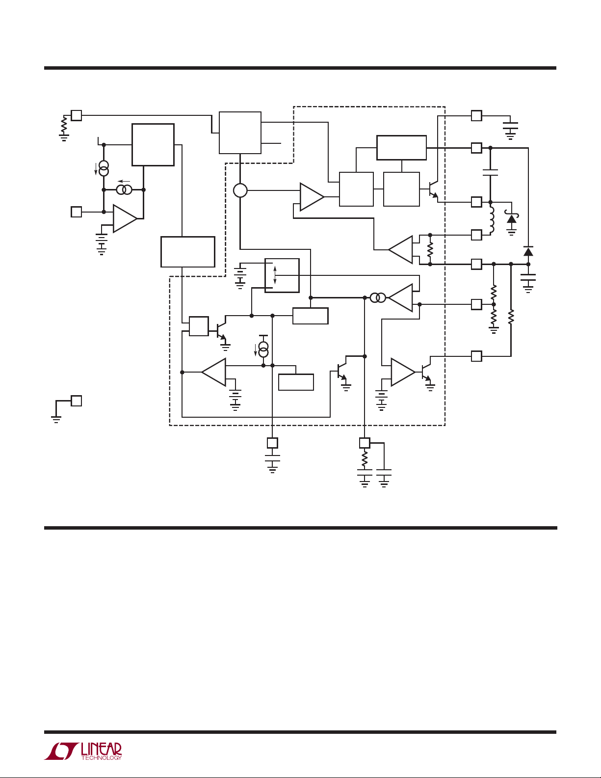
BLOCK DIAGRAM
/SYNC
R
T
R3
3μA
SHDN
1.28V
GND
V
IN1
+
INTERNAL
REGULATOR
AND
REFERENCE
7μA
+
–
SHUTDOWN
COMPARATOR
UNDERVOLTAGE
POR
TSD
S
RQ
SOFT-START
RESET
COMPARATOR
OSCILLATOR
AND
AGC
SLOPE
COMPENSATION
3
+
0.8V
3.25A
–
+
+
80mV
CLK1
CLK2
LOWEST
VOLTAGE
SS
ONE CHANNEL
–
+
VC CLAMP
SS CLAMP
LT3510
V
IN
C
DROPOUT
ENHANCEMENT
PRE
S
R
Q
DRIVER
CIRCUITRY
+
–
+
–
POWER GOOD
COMPARATOR
–
+
+
0.72V
V
C
BST
SW
IND
V
OUT
PGOOD
3510 BD
C3
D
L1
D
C
FB
R1
R2
C
Figure 1. Block Diagram (One of Two Switching Regulators Shown)
APPLICATIONS INFORMATION
The LT3510 is dual channel, constant frequency, current
mode buck converter with internal 2A switches. Each
channel is identical with a common shutdown pin, internal
regulator, oscillator, undervoltage detect, thermal shutdown
and power-on reset.
If the SHDN pin is taken below its 1.28V threshold the
LT3510 will be placed in a low quiescent current mode.
In this mode the LT3510 typically draws 9μA from V
and <1μA from V
with a typical sink capability of 50μA for V
. In shutdown mode the PG is active
IN2
voltage
IN1
greater than 2V.
IN1
When the SHDN pin is opened or driven above 1.28V,
the internal bias circuits turn on generating an internal
regulated voltage, 0.8V
, 0.975V RT/SYNC references,
FB
and a POR signal which sets the soft-start latch.
As the R
/SYNC pin reaches its 0.975V regulation point,
T
the internal oscillator will start generating two clock signals 180° out of phase for each regulator at a frequency
determined by the resistor from the R
/SYNC pin to ground.
T
Alternatively, if a synchronization signal is detected by the
LT3510 at the R
/SYNC pin, clock signals 180° out of phase
T
3510fc
9

LT3510
APPLICATIONS INFORMATION
will be generated at the incoming frequency on the rising
edge of the synchronization pulse with switch 1 in phase
with the synchronization signal. In addition, the internal
slope compensation will be automatically adjusted to prevent subharmonic oscillation during synchronization.
The two regulators are constant frequency, current mode
step-down converters. Current mode regulators are controlled by an internal clock and two feedback loops that
control the duty cycle of the power switch. In addition to
the normal error amplifi er, there is a current sense amplifi er
that monitors switch current on a cycle-by-cycle basis.
This technique means that the error amplifi er commands
current to be delivered to the output rather than voltage.
A voltage fed system will have low phase shift up to the
resonant frequency of the inductor and output capacitor,
then an abrupt 180°, shift will occur. The current fed system will have 90° phase shift at a much lower frequency,
but will not have the additional 90° shift until well beyond
the LC resonant frequency. This makes it much easier to
frequency compensate the feedback loop and also gives
much quicker transient response.
The Block Diagram in Figure 1 shows only one of the
switching regulators whose operation will be discussed
below. The additional regulator will operate in a similar
manner with the exception that its clock will be 180° out
of phase with the other regulator.
When, during power up, the POR signal sets the soft-start
latch, both SS pins will be discharged to ground to ensure
proper start-up operation. When the SS pin voltage drops
below 80mV, the V
pin is driven low disabling switching
C
and the soft-start latch is reset. Once the latch is reset the
soft-start capacitor starts to charge with a typical value
of 3.25μA.
As the voltage rises above 80mV on the SS pin, the V
pin
C
will be driven high by the error amplifi er. When the voltage
on the V
pin exceeds 0.7V, the clock set pulse sets the
C
driver fl ip-fl op which turns on the internal power NPN
switch. This causes current from V
, through the NPN
IN
switch, inductor and internal sense resistor, to increase.
When the voltage drop across the internal sense resistor
exceeds a predetermined level set by the voltage on the
pin, the fl ip-fl op is reset and the internal NPN switch
V
C
is turned off. Once the switch is turned off the inductor
will drive the voltage at the SW pin low until the external
Schottky diode starts to conduct, decreasing the current
in the inductor. The cycle is repeated with the start of each
clock cycle. However, if the internal sense resistor voltage
exceeds the predetermined level at the start of a clock cycle,
the fl ip-fl op will not be set resulting in a further decrease in
inductor current. Since the output current is controlled by
voltage, output regulation is achieved by the error
the V
C
amplifi er continually adjusting the V
pin voltage.
C
The error amplifi er is a transconductance amplifi er that
compares the FB voltage to the lowest voltage present at
either the SS pin or an internal 0.8V reference. Compensation of the loop is easily achieved with a simple capacitor
or series resistor/capacitor from the V
pin to ground.
C
Since the SS pin is driven by a constant current source, a
single capacitor on the soft-start pin will generate controlled
linear ramp on the output voltage.
If the current demanded by the output exceeds the maximum current dictated by the V
pin clamp, the SS pin
C
will be discharged, lowering the regulation point until the
output voltage can be supported by the maximum current.
When overload is removed, the output will soft-start from
the overload regulation point.
undervoltage detection or thermal shutdown will
V
IN1
set the soft-start latch, resulting in a complete soft-start
sequence.
The switch driver operates from either the V
or BST volt-
IN
age. An external diode and capacitor are used to generate
a drive voltage higher than V
to saturate the output NPN
IN
and maintain high effi ciency. If the BST capacitor voltage
is suffi cient, the switch is allowed to operate to 100% duty
cycle. If the boost capacitor discharges towards a level
insuffi cient to drive the output NPN, a BST pin comparator forces a minimum cycle off time, allowing the boost
capacitor to recharge.
A power good comparator with 30mV of hysteresis trips
at 90% of regulated output voltage. The PG output is an
open-collector NPN that is off when the output is in regulation allowing a resistor to pull the PG pin to a desired
voltage.
10
3510fc

APPLICATIONS INFORMATION
LT3510
Choosing the Output Voltage
The output voltage is programmed with a resistor divider
between the output and the FB pin. Choose the 1% resistors according to:
RR
12
⎛
OUT
•
⎜
⎝
08
.
⎞
1=
–
⎟
⎠
V
V
R2 should be 10k or less to avoid bias current errors. Reference designators refer to the Block Diagram in Figure 1.
Choosing the Switching Frequency
The LT3510 switching frequency is set by resistor R3 in
Figure 1. The R
Setting resistor R3 sets the current in the R
/SYNC pin is internally regulated at 0.975V.
T
/SYNC pin
T
which determines the oscillator frequency as illustrated
in Figure 2.
The switching frequency is typically set as high as possible to reduce overall solution size. The LT3510 employs
techniques to enhance dropout at high frequencies but
effi ciency and maximum input voltage decrease due to
switching losses and minimum switch on times. The
maximum recommended frequency can be approximated
by the equation:
1600
1400
1200
1000
800
600
FREQUENCY (kHz)
400
200
100
Figure 2. Frequency and Phase vs RT/SYNC Resistance
FREQUENCY
PHASE
0 20 40 60 80 100 120 140
RESISTANCE (kΩ)
3510 F02
190
185
180
PHASE (DEG)
175
170
165
160
155
150
The following example along with the data in Table 1
illustrates the tradeoffs of switch frequency selection.
Example.
= 25V, V
V
IN
OUT
= 3.3V, I
OUT
= 2.5A,
Temperature = 0°C to 85°C
t
ON(MIN)
Characteristics graph), V
Max Frequency
= 200ns (85°C from the Typical Performance
= 0.6V, V
D
..
+
33 06
–. .
25 04 06
+
= 0.4V (85°C)
SW
1
•~=
200e-9
750
kkHz
Frequency Hz
()
=
+
OUT D
VV Vt
–
IN SW D ON MIN
+
•
1
()
VV
where VD is the forward voltage drop of the catch diode (D1
Figure 2), V
and t
ON(MIN)
is the voltage drop of the internal switch,
SW
in the minimum on time of the switch, all at
maximum load current.
Table 1. Effi ciency and Size Comparisons for Different R
Output
FREQUENCY RT/SYNC
1.2MHz 20.5k 79.0% 16 1.5μH 22μF 63mm
1.0MHz 26.7k 80.9% 18 2.2μH 47μF 66mm
750kHz 38.3k 81.2% 22 3.3μH 47μF 66mm
500kHz 61.9k 82.0% 24 4.7μH 47μF 66mm
250kHz 133k 83.9% 24 10μH 100μF 172mm
†
V
is defi ned as the highest input voltage that maintains constant output voltage ripple.
IN(MAX)
*Inductor and capacitor values chosen for stability and constant ripple current.
EFFICIENCY
V
= 12V V
VIN1/2
/~( )42 2
R SYNC k Figure
T
Input Voltage Range
Once the switching frequency has been determined, the
input voltage range of the regulator can be determined.
The minimum input voltage is determined by either the
LT3510’s minimum operating voltage of ~2.8V, or by its
Values. 3.3V
RT/SYNC
†
IN(MAX)
L* C* L + C AREA
2
2
2
2
2
3510fc
11

LT3510
APPLICATIONS INFORMATION
maximum duty cycle. The duty cycle is the fraction of time
that the internal switch is on during a clock cycle. Unlike
most fi xed frequency regulators, the LT3510 will not switch
off at the end of each clock cycle if there is suffi cient voltage across the boost capacitor (C3 in Figure 1) to fully
saturate the output switch. Forced switch off for a minimum
time will only occur at the end of a clock cycle when the
boost capacitor needs to be recharged. This operation
has the same effect as lowering the clock frequency for a
fi xed off time, resulting in a higher duty cycle and lower
minimum input voltage. The resultant duty cycle depends
on the charging times of the boost capacitor and can be
approximated by the following equation:
DC
MAX
=
1
+11
B
where B is 2A divided by the typical boost current from
the Electrical Characteristics.
This leads to a minimum input voltage of:
VV
+
V
IN MIN
OUT D
DC
MAX
VV
–=
+
DSW()
6.0
V
= 3.3V
OUT
5.5
5.0
4.5
VOLTAGE (V)
4.0
3.5
3.0
1
Figure 3. Minimum Input Voltage vs Load Current
START-UP
RUNNING
10 100 1000 10000
CURRENT (mA)
3510 F03
Example:
V
OUT
= 3.3V, I
= 1A, Frequency = 1MHz, Temperature
OUT
= 25°C
= 0.1V, B = 40 (from boost characteristics specifi ca-
V
SW
tion), V
DC
MAX
= 0.4V, t
D
=
1
ON(MIN)
1
+
1
=
98
= 200ns
%
40
where VSW is the voltage drop of the internal switch.
Figure 3 shows a typical graph of minimum input voltage
vs load current for the 3.3V and 1.8V application on the
fi rst page of this data sheet. The maximum input voltage
is determined by the absolute maximum ratings of the V
IN
and BST pins and by the frequency and minimum duty
cycle. The minimum duty cycle is defi ned as :
DC
MIN
= t
ON(MIN)
• Frequency
Maximum input voltage as:
VV
+
OUT D
DC
MIN
VV
–=
+
DSW()
V
IN MAX
Note that the LT3510 will regulate if the input voltage is
taken above the calculated maximum voltage as long as
maximum ratings of the V
and BST pins are not violated.
IN
However operation in this region of input voltage will exhibit
pulse skipping behavior.
+
33 04
V
IN MIN
()
DC t f
MIN MIN ON
V
()
IN MAX
..
=
==
33
=
098
.
()
004
+
.
0 200
.
04 0
–. .
0 200
•.
.
04 01 182
–. . .+= V
11348
+
=
V
.
Inductor Selection and Maximum Output Current
A good fi rst choice for the inductor value is:
–•
VV V
()
IN OUT OUT
L
=
•
Vf
IN
where f is frequency in MHz and L is in μH.
With this value the maximum load current will be ~2A,
independent of input voltage. The inductor’s RMS current
rating must be greater than your maximum load current
12
3510fc

APPLICATIONS INFORMATION
LT3510
and its saturation current should be about 30% higher. To
keep effi ciency high, the series resistance (DCR) should
be less than 0.05Ω.
For applications with a duty cycle of about 50%, the inductor value should be chosen to obtain an inductor ripple
current less than 40% of peak switch current.
Of course, such a simple design guide will not always
result in the optimum inductor for your application. A
larger value provides a slightly higher maximum load
current, and will reduce the output voltage ripple. If your
load is lower than 2A, then you can decrease the value of
the inductor and operate with higher ripple current. This
allows you to use a physically smaller inductor, or one
with a lower DCR resulting in higher effi ciency.
The current in the inductor is a triangle wave with an
average value equal to the load current. The peak switch
current is equal to the output current plus half the peak-topeak inductor ripple current. The LT3510 limits its switch
current in order to protect itself and the system from
overload faults. Therefore, the maximum output current
that the LT3510 will deliver depends on the current limit,
the inductor value, switch frequency, and the input and
output voltages. The inductor is chosen based on output
current requirements, output voltage ripple requirements,
size restrictions and effi ciency goals.
2.5A over the entire duty cycle range. The maximum output
current is a function of the chosen inductor value:
II
ΔΔ
II
OUT MAX LIM
()
LL
–.–==
25
2
2
If the inductor value is chosen so that the ripple current
is small, then the available output current will be near the
switch current limit.
One approach to choosing the inductor is to start with the
simple rule given above, look at the available inductors
and choose one to meet cost or space goals. Then use
these equations to check that the LT3510 will be able to
deliver the required output current. Note again that these
equations assume that the inductor current is continuous.
Discontinuous operation occurs when I
/2 as calculated above.
I
L
is less than
OUT
Figure 4 illustrates the inductance value needed for a 3.3V
output with a maximum load capability of 2A. Referring
to Figure 4, an inductor value between 3.3μH and 4.7μH
will be suffi cient for a 15V input voltage and a switch
frequency of 750kHz. There are several graphs in the
Typical Performance Characteristics section of this data
sheet that show inductor selection as a function of input
voltage and switch frequency for several popular output
voltages and output ripple currents. Also, low inductance
When the switch is off, the inductor sees the output voltage plus the catch diode drop. This gives the peak-to-peak
ripple current in the inductor:
1–
DC V V
()
ΔI
=
L
+
()
OUT D
•
Lf
where f is the switching frequency of the LT3510 and L
is the value of the inductor. The peak inductor and switch
current is:
I
Δ
III
SW PK
==+
()
LPK OUT
L
2
To maintain output regulation, this peak current must be
. I
less than the LT3510’s switch current limit I
LIM
LIM
is
1500
L = 2.2μH
1250
1000
750
FREQUENCY (kHz)
500
250
10
Figure 4. Inductor Values for 2A Maximum Load Current
vs Frequency and Input Voltage
15 17.5 20
12.5
INPUT VOLTAGE (V)
L = 3.3μH
L = 4.7μH
V
= 5V
OUT
I
RIPPLE
L = 6.8μH
L = 10μH
22.5 25
= 1A
3510 F04
3510fc
13

LT3510
APPLICATIONS INFORMATION
may result in discontinuous mode operation, which is
okay, but further reduces maximum load current. For
details of maximum output current and discontinuous
mode operation, see Linear Technology Application Note
44. Finally, for duty cycles greater than 50% (V
> 0.5), there is a minimum inductance required to avoid
subharmonic oscillations. See Application Note 19 for
more information.
Input Capacitor Selection
Bypass the inputs of the LT3510 circuit with a 4.7μF or
higher ceramic capacitor of X7R or X5R type. A lower
value or a less expensive Y5V type can be used if there
is additional bypassing provided by bulk electrolytic or
tantalum capacitors. The following paragraphs describe
the input capacitor considerations in more detail.
Step-down regulators draw current from the input supply in
pulses with very fast rise and fall times. The input capacitor is required to reduce the resulting voltage ripple at the
LT3510 and to force this very high frequency switching
current into a tight local loop, minimizing EMI. The input
capacitor must have low impedance at the switching frequency to do this effectively, and it must have an adequate
ripple current rating. With two switchers operating at the
same frequency but with different phases and duty cycles,
calculating the input capacitor RMS current is not simple.
However, a conservative value is the RMS input current for
the channel that is delivering most power (V
This is given by:
I
CIN RMS
()
IV VV
OUT OUT IN OUT
=
•–
()
V
IN
OUT/VIN
• I
OUT
I
OUT
<
2
OUT
).
ments of the input capacitor. Determine the worst-case
condition for input ripple current and then size the input
capacitor such that it reduces input voltage ripple to an
acceptable level. Typical values for input capacitors run
from 10μF at low frequencies to 2.2μF at higher frequencies.
The combination of small size and low impedance (low
equivalent series resistance or ESR) of ceramic capacitors
make them the preferred choice. The low ESR results in
very low voltage ripple and the capacitors can handle plenty
of ripple current. They are also comparatively robust and
can be used in this application at their rated voltage. X5R
and X7R types are stable over temperature and applied
voltage, and give dependable service. Other types (Y5V and
Z5U) have very large temperature and voltage coeffi cients
of capacitance, so they may have only a small fraction of
their nominal capacitance in your application. While they
will still handle the RMS ripple current, the input voltage
ripple may become fairly large, and the ripple current may
end up fl owing from your input supply or from other bypass capacitors in your system, as opposed to being fully
sourced from the local input capacitor. An alternative to a
high value ceramic capacitor is a lower value along with
a larger electrolytic capacitor, for example a 1μF ceramic
capacitor in parallel with a low ESR tantalum capacitor.
For the electrolytic capacitor, a value larger than 10μF will
be required to meet the ESR and ripple current requirements. Because the input capacitor is likely to see high
surge currents when the input source is applied, tantalum
capacitors should be surge rated. The manufacturer may
also recommend operation below the rated voltage of the
capacitor. Be sure to place the 1μF ceramic as close as
possible to the V
noise immunity.
and GND pins on the IC for optimal
IN
and is largest when VIN = 2V
the second, lower power channel draws input current,
the input capacitor’s RMS current actually decreases as
the out-of-phase current cancels the current drawn by the
higher power channel. Considering that the maximum load
current from a single channel is ~2A, RMS ripple current
will always be less than 1A.
The frequency, VIN to V
rent requirement of the LT3510 along with the input supply
source impedance, determine the energy storage require-
ratio, and maximum load cur-
OUT
(50% duty cycle). As
OUT
14
When the LT3510’s input supplies are operated at different
input voltages, an input capacitor sized for that channel
should be placed as close as possible to the respective
pins.
V
IN
A fi nal caution regarding the use of ceramic capacitors
at the input. A ceramic input capacitor can combine with
stray inductance to form a resonant tank circuit. If power
is applied quickly (for example by plugging the circuit
into a live power source) this tank can ring, doubling the
input voltage and damaging the LT3510. The solution is to
3510fc

APPLICATIONS INFORMATION
LT3510
either clamp the input voltage or dampen the tank circuit
by adding a lossy capacitor in parallel with the ceramic
capacitor. For details, see Application Note 88.
Output Capacitor Selection
Typically step-down regulators are easily compensated with
an output crossover frequency that is 1/10 of the switching frequency. This means that the time that the output
capacitor must supply the output load during a transient
step is ~2 or 3 switching periods. With an allowable 5%
drop in output voltage during the step, a good starting
value for the output capacitor can be expressed by:
C
VOUT
Max Load Step
=
Frequency V
•. •005
OUT
Example:
= 3.3V, Frequency = 1MHz, Max Load Step = 2A
V
OUT
C
==
VOUT
eV
16 005 33
2
•. •.
12
F
μ
The calculated value is only a suggested starting value.
Increase the value if transient response needs improvement
or reduce the capacitance if size is a priority.
The output capacitor fi lters the inductor current to generate
an output with low voltage ripple. It also stores energy in
order to satisfy transient loads and to stabilize the LT3510’s
control loop. The switching frequency of the LT3510 determines the value of output capacitance required. Also, the
current mode control loop doesn’t require the presence
of output capacitor series resistance (ESR). For these
reasons, you are free to use ceramic capacitors to achieve
very low output ripple and small circuit size.
Estimate output ripple with the following equations:
V
RIPPLE
= ΔIL/(8f C
) for ceramic capacitors,
OUT
and
V
= ΔIL ESR for electrolytic capacitors (tantalum
RIPPLE
and aluminum)
where ΔI
is the peak-to-peak ripple current in the
L
inductor.
The RMS content of this ripple is very low, and the RMS
current rating of the output capacitor is usually not of
concern.
Another constraint on the output capacitor is that it must
have greater energy storage than the inductor; if the stored
energy in the inductor is transferred to the output, you
would like the resulting voltage step to be small compared
to the regulation voltage. For a 5% overshoot, this requirement becomes:
I
LIM
OUT
2
⎞
⎟
⎠
CL
⎛
>
10
OUT
⎜
V
⎝
Finally, there must be enough capacitance for good transient
performance. The last equation gives a good starting point.
Alternatively, you can start with one of the designs in this
data sheet and experiment to get the desired performance.
This topic is covered more thoroughly in the section on
loop compensation.
The high performance (low ESR), small size and robustness
of ceramic capacitors make them the preferred type for
LT3510 applications. However, all ceramic capacitors are
not the same. As mentioned above, many of the high value
capacitors use poor dielectrics with high temperature and
voltage coeffi cients. In particular, Y5V and Z5U types lose
a large fraction of their capacitance with applied voltage
and temperature extremes. Because the loop stability and
transient response depend on the value of C
, you may
OUT
not be able to tolerate this loss. Use X7R and X5R types.
You can also use electrolytic capacitors. The ESRs of most
aluminum electrolytics are too large to deliver low output
ripple. Tantalum and newer, lower ESR organic electrolytic
capacitors intended for power supply use, are suitable
and the manufacturers will specify the ESR. The choice of
capacitor value will be based on the ESR required for low
ripple. Because the volume of the capacitor determines
its ESR, both the size and the value will be larger than a
ceramic capacitor that would give you similar ripple performance. One benefi t is that the larger capacitance may
give better transient response for large changes in load
current. Table 2 lists several capacitor vendors.
3510fc
15

LT3510
APPLICATIONS INFORMATION
Table 2
VENDOR TYPE SERIES
Taiyo Yuden Ceramic X5R, X7R
AVX Ceramic X5R, X7R
Tantalum
Kemet Tantalum
TA Organic
AL Organic
Sanyo TA/AL Organic POSCAP
Panasonic AL Organic SP CAP
TDK Ceramic X5R, X7R
T491, T494, T495
T520
A700
Catch Diode
The diode D1 conducts current only during switch off
time. Use a Schottky diode to limit forward voltage drop to
increase effi ciency. The Schottky diode must have a peak
reverse voltage that is equal to regulator input voltage and
sized for average forward current in normal operation.
Average forward current can be calculated from:
I
OUT
V
VV
•–=
()
IN
IN OUT()
I
D AVG
The only reason to consider a larger diode is the worstcase condition of a high input voltage and shorted output.
With a shorted condition, diode current will increase to a
typical value of 3A, determined by the peak switch current
limit of the LT3510. This is safe for short periods of time,
but it would be prudent to check with the diode manufacturer if continuous operation under these conditions
can be tolerated.
BST Pin Considerations
The capacitor and diode tied to the BST pin generate
a voltage that is higher than the input voltage. In most
cases a 0.47μF capacitor and fast switching diode (such
as the CMDSH-3 or FMMD914) will work well. Almost
any type of fi lm or ceramic capacitor is suitable, but the
ESR should be <1Ω to ensure it can be fully recharged
during the off time of the switch. The capacitor value can
be approximated by:
IDC
C
=
BST
OUT MAX
•– •
BV V f
()
OUT BST MIN
•
()
()
where I
V
BST(MIN)
OUT(MAX)
is the minimum boost voltage to fully saturate
is the maximum load current, and
the switch.
Figure 5 shows four ways to arrange the boost circuit. The
BST pin must be more than 1.4V above the SW pin for
full effi ciency. Generally, for outputs of 3.3V and higher
the standard circuit (Figure 5a) is the best. For outputs
between 2.8V and 3.3V, replace the D2 with a small Schottky
diode such as the PMEG4005. For lower output voltages
the boost diode can be tied to the input (Figure 5b). The
circuit in Figure 5a is more effi cient because the BST
pin current comes from a lower voltage source. Figure
5c shows the boost voltage source from available DC
sources that are greater than 3V. The highest effi ciency is
attained by choosing the lowest boost voltage above 3V.
For example, if you are generating 3.3V and 1.8V and the
3.3V is on whenever the 1.8V is on, the 1.8V boost diode
can be connected to the 3.3V output. In any case, you
must also be sure that the maximum voltage at the BST
pin is less than the maximum specifi ed in the Absolute
Maximum Ratings section.
The boost circuit can also run directly from a DC voltage
that is higher than the input voltage by more than 3V, as
in Figure 5d. The diode is used to prevent damage to the
LT3510 in case V
is held low while VIN is present. The
X
circuit saves several components (both BST pins can be
tied to D2). However, effi ciency may be lower and dissipation in the LT3510 may be higher. Also, if V
is absent, the
X
LT3510 will still attempt to regulate the output, but will do
so with very low effi ciency and high dissipation because
the switch will not be able to saturate, dropping 1.5V to
2V in conduction.
The minimum input voltage of an LT3510 application is
limited by the minimum operating voltage (<3V) and by
the maximum duty cycle as outlined above. For proper
start-up, the minimum input voltage is also limited by
the boost circuit. If the input voltage is ramped slowly, or
the LT3510 is turned on with its SS pin when the output
is already in regulation, then the boost capacitor may not
be fully charged. Because the boost capacitor is charged
with the energy stored in the inductor, the circuit will rely
on some minimum load current to get the boost circuit
running properly. This minimum load will depend on
3510fc
16

(5d)(5c)
APPLICATIONS INFORMATION
LT3510
D2
V
BST
V
BST(MAX)
V
IN
– VSW = V
= VIN+ V
OUT
OUT
BST
GND
SW
IND
V
OUT
V
IN
LT3510
C3
D2
V
OUT
(5a)
= VIN + V
= 3V
D2
BST
V
IN
LT3510
X
X
GND
SW
IND
V
OUT
C3
V
< 3V
OUT
VX = LOWEST V
OR V
> 3V
OUT
V
BST
V
BST(MAX)
V
X(MIN)
IN
V
IN
– VSW = V
Figure 5. BST Pin Considerations
input and output voltages, and on the arrangement of the
boost circuit. The Typical Performance Characteristics
section shows plots of the minimum load current to start
and to run as a function of input voltage for 3.3V and 5V
outputs. In many cases the discharged output capacitor
will present a load to the switcher which will allow it to
start. The plots show the worst-case situation where V
IN
is
ramping very slowly. Use a Schottky diode for the lowest
start-up voltage.
Frequency Compensation
The LT3510 uses current mode control to regulate the
output. This simplifi es loop compensation. In particular, the
LT3510 does not require the ESR of the output capacitor
for stability so you are free to use ceramic capacitors to
achieve low output ripple and small circuit size.
Frequency compensation is provided by the components
tied to the V
pin. Generally a capacitor and a resistor in
C
series to ground determine loop gain. In addition, there
is a lower value capacitor in parallel. This capacitor is not
C3
V
< 3V
OUT
V
V
BST
V
BST(MAX)
IN
– VSW = V
= 2 •V
BST
GND
SW
IND
V
OUT
V
IN
LT3510
IN
IN
(5b)
D2
VX > VIN + 3V
BST
V
IN
V
– VSW = V
BST
V
BST(MAX)
V
X(MIN)
= V
= VIN + 3V
V
IN
LT3510
X
X
GND
SW
IND
V
V
OUT
3510 F05
OUT
< 3V
part of the loop compensation but is used to fi lter noise
at the switching frequency.
Loop compensation determines the stability and transient
performance. Designing the compensation network is a bit
complicated and the best values depend on the application
and in particular the type of output capacitor. A practical
approach is to start with one of the circuits in this data
sheet that is similar to your application and tune the compensation network to optimize the performance. Stability
should then be checked across all operating conditions,
including load current, input voltage and temperature.
The LT1375 data sheet contains a more thorough discussion of loop compensation and describes how to test the
stability using a transient load.
Figure 6 shows an equivalent circuit for the LT3510 control
loop. The error amp is a transconductance amplifi er with
fi nite output impedance. The power section, consisting of
the modulator, power switch and inductor, is modeled as
a transconductance amplifi er generating an output current proportional to the voltage at the V
pin. Note that
C
3510fc
17

LT3510
APPLICATIONS INFORMATION
LT3510
CURRENT MODE
POWER STAGE
= 2.2mho
g
m
V
C
R
C
C
C
3.6M
C
F
Figure 6. Model for Loop Response
= 275μmho
g
m
ERROR
AMP
SW
C
R1 ESR
–
+
FB
+
0.8V
R2
PL
TANTALUM
OR
POLYMER
OUTPUT
C1 C1
CERAMIC
3510 F06
the output capacitor integrates this current, and that the
capacitor on the V
pin (CC) integrates the error ampli-
C
fi er output current, resulting in two poles in the loop. In
most cases a zero is required and comes from either the
output capacitor ESR or from a resistor in series with C
.
C
This simple model works well as long as the value of the
inductor is not too high and the loop crossover frequency
is much lower than the switching frequency. A phase lead
capacitor (C
) across the feedback divider may improve
PL
the transient response.
Synchronization
/SYNC pin can be used to synchronize the regulators
The R
T
to an external clock source. Driving the RT/SYNC resistor
with a clock source triggers the synchronization detection
circuitry. Once synchronization is detected, the rising edge
of SW1 will be synchronized to the rising edge of the
RT/SYNC pin signal. An AGC loop will adjust the internal
oscillators to maintain a 180 degree phase between SW1
and SW2, and also adjust slope compensation to avoid
subharmonic oscillation.
The synchronizing clock signal input to the LT3510 must
have a frequency between 250kHz and 1.5MHz, a duty
cycle between 20% and 80%, a low state below 0.5V and
a high state above 1.6V. Synchronization signals outside
of these parameters will cause erratic switching behavior.
The RT/SYNC resistor should be set such that the free
running frequency ((V
RT/SYNC
– V
SYNCLO
)/R
RT/SYNC
) is
approximately equal to the synchronization frequency. If
the synchronization signal is halted, the synchronization
detection circuitry will timeout in typically 10μs at which
V
OUT1
LT3510 SYNCHRONIZATION
PG1
RT/SYNC
Figure 7. Synchronous Signal Powered from Regulator’s Output
V
CC
CIRCUITRY
CLK
3510 F07
time the LT3510 reverts to the free-running frequency
based on the current through R
/SYNC. If the RT/SYNC
T
resistor is held above 2V at any time, switching will be
disabled.
If the synchronization signal is not present during regulator start-up (for example, the synchronization circuitry is
powered from the regulator output) the R
/SYNC pin must
T
see an equivalent resistance to ground between 15.4k and
133k until the synchronization circuitry is active for proper
start-up operation.
If the synchronization signal powers up in an undetermined
state (V
, VOH, Hi-Z), connect the synchronization clock
OL
to the LT3510 as shown in Figure 7. The circuit as shown
will isolate the synchronization signal when the output
voltage is below 90% of the regulated output. The LT3510
will start-up with a switching frequency determined by the
resistor from the R
/SYNC pin to ground.
T
If the synchronization signal powers up in a low impedance
state (V
), connect a resistor between the RT/SYNC pin
OL
and the synchronizing clock. The equivalent resistance
seen from the R
/SYNC pin to ground will set the start-up
T
frequency.
3510fc
18

APPLICATIONS INFORMATION
LT3510
If the synchronization signal powers up in a high impedance
state (Hi-Z), connect a resistor from the R
ground. The equivalent resistance seen from the R
/SYNC pin to
T
/SYNC
T
pin to ground will set the start-up frequency.
If the synchronization signal changes between high and
low impedance states during power up (V
, Hi-Z), connect
OL
the synchronization circuitry to the LT3510 as shown in
the Typical Applications section. This will allow the LT3510
to start-up with a switching frequency determined by the
equivalent resistance from the R
/SYNC pin to ground.
T
Shutdown and Undervoltage Lockout
Figure 8 shows how to add undervoltage lockout (UVLO)
to the LT3510. Typically, UVLO is used in situations where
the input supply is current limited, or has a relatively high
source resistance. A switching regulator draws constant
power from the source, so source current increases as
source voltage drops. This looks like a negative resistance
load to the source and can cause the source to current limit
or latch low under low source voltage conditions. UVLO
prevents the regulator from operating at source voltages
where these problems might occur.
An internal comparator will force the part into shutdown
below the minimum V
of 2.8V. This feature can be
IN1
used to prevent excessive discharge of battery-operated
systems.
Since V
not monitored, care must be taken to insure that V
supplies the output stage of channel 2 and is
IN2
IN2
is
present before channel 2 is allowed to switch.
If an adjustable UVLO threshold is required, the SHDN
pin can be used. The threshold voltage of the SHDN
pin comparator is 1.28V. A 3μA internal current source
LT3510
V
V
> 2.8V
IN1
V
OR V
IN1
IN2
IN1
1.28V
–
+
INTERNAL
REGULATOR
3510 F08
+
7μA
3μA
R1
SHDN
R2C1
defaults the open-pin condition to be operating (see Typical
Performance Characteristics). Current hysteresis is added
above the SHDN threshold. This can be used to set voltage
hysteresis of the UVLO using the following:
VV
–
HL
R
1
=
R
2
A
7
μ
128
–.
H
128
R
1
.
A
3
+
μ
=
V
VH = Turn-on threshold
= Turn-off threshold
V
L
Example: switching should not start until the input is above
4.75V and is to stop if the input falls below 3.75V.
= 4.75V
V
H
= 3.75V
V
L
475 375
R
R
.–.
1
=≅
2
=
A
7
μ
128
.
475 128
.–.
k
143
+
143
3
μAA
k
k≅ 47
Keep the connections from the resistors to the SHDN
pin short and make sure that the interplane or surface
capacitance to switching nodes is minimized. If high resistor values are used, the SHDN pin should be bypassed
with a 1nF capacitor to prevent coupling problems from
the switch node.
Soft-Start
The output of the LT3510 regulates to the lowest voltage
present at either the SS pin or an internal 0.8V reference.
A capacitor from the SS pin to ground is charged by an
internal 3.25μA current source resulting in a linear output
ramp from 0V to the regulated output whose duration is
given by:
CV
•..08
t
RAMP
=
SS
325μ
A
Figure 8. Undervoltage Lockout
3510fc
19

LT3510
APPLICATIONS INFORMATION
At power-up, a reset signal sets the soft-start latch and
discharges both SS pins to approximately 0V to ensure
proper start-up. When both SS pins are fully discharged
the latch is reset and the internal 3.25μA current source
starts to charge the SS pin.
When the SS pin voltage is below 50mV, the VC pin is pulled
low which disables switching. This allows the SS pin to be
used as an individual shutdown for each channel.
As the SS pin voltage rises above 50mV, the VC pin is released and the output is regulated to the SS voltage. When
the SS pin voltage exceeds the internal 0.8V reference, the
output is regulated to the reference. The SS pin voltage
will continue to rise until it is clamped at 2V.
In the event of a V
undervoltage lockout, the SHDN
IN1
pin driven below 1.28V, or the internal die temperature
exceeding its maximum rating during normal operation, the
soft-start latch is set, triggering a start-up sequence.
In addition, if the load exceeds the maximum output switch
current, the output will start to drop causing the VC pin
clamp to be activated. As long as the VC pin is clamped,
the SS pin will be discharged. As a result, the output will
be regulated to the highest voltage that the maximum
output current can support. For example, if a 6V output
is loaded by 1Ω the SS pin will drop to 0.4V, regulating
the output at 3V ( 3A • 1Ω ). Once the overload condition
is removed, the output will soft-start from the temporary
voltage level to the normal regulation point.
Since the SS pin is clamped at 2V and has to discharge
to 0.8V before taking control of regulation, momentary
overload conditions will be tolerated without a soft-start
recovery. The typical time before the SS pin takes control
is:
•.=12
CV
t
SS CONTROL
()
SS
700μ
A
Power Good Indicators
The PG pin is the open-collector output of an internal
comparator. The comparator compares the FB pin voltage
to 90% of the reference voltage with 30mV of hysteresis.
The PG pin has a sink capability of 800μA when the FB pin
is below the threshold and can withstand 25V when the
threshold is exceeded. The PG pin is active (sink capability
is reduced in shutdown and undervoltage lockout mode)
as long as the V
pin voltage exceeds 1V.
IN1
Output Tracking/Sequencing
Complex output tracking and sequencing between channels can be implemented using the LT3510’s SS and PG
pins. Figure 9 shows several confi gurations for output
tracking/sequencing for a 3.3V and 1.8V application.
Independent soft-start for each channel is shown in
Figure 9a. The output ramp time for each channel is set
by the soft-start capacitor as described in the soft-start
section.
Ratiometric tracking is achieved in Figure 9b by connecting
both SS pins together. In this confi guration, the SS pin
source current is doubled (6.5μA) which must be taken
into account when calculating the output rise time.
By connecting a feedback network from V
pin with the same ratio that sets V
voltage, absolute
OUT2
to the SS2
OUT1
tracking shown in Figure 9c is implemented. The minimum
value of the top feedback resistor (R1) should be set such
that the SS pin can be driven all the way to ground with
700μA of sink current when V
In addition, a small V
OUT2
is at its regulated voltage.
OUT1
voltage offset will be present
due to the SS2 3.25μA source current. This offset can be
corrected for by slightly reducing the value of R2.
Figure 9d illustrates output sequencing. When V
OUT1
is
within 10% of its regulated voltage, PG1 releases the SS2
soft-start pin allowing V
to soft-start. In this case PG1
OUT2
will be pulled up to 2V by the SS pin. If a greater voltage
is needed for PG1 logic, a pull-up resistor to V
OUT1
can
be used. This will decrease the soft-start ramp time and
increase tolerance to momentary shorts.
If precise output ramp up and down is required, drive the
SS pins as shown in Figure 9e. The minimum value of
resistor (R3) should be set such that the SS pin can be
driven all the way to ground with 700μA of sink current
during power-up and fault conditions.
Multiple Input Voltages
For applications requiring large inductors due to high V
to V
ratios, a 2-stage step-down approach may reduce
OUT
3510fc
IN
20

APPLICATIONS INFORMATION
LT3510
Independent Start-Up Ratiometric Start-Up
V
OUT1
0.5V/DIV
PG1
V
OUT2
0.5V/DIV
PG2 PG2
0.1μF
0.22μF
SS1
SS2
5ms/DIV
LT3510
(9a)
V
V
OUT1
PG1
OUT2
PG2
3.3V
0.1μF
1.8V
10ms/DIV 10ms/DIV
SS1
LT3510
SS2
(9b)
Absolute Start-Up
V
OUT1
0.5V/DIV
PG1PG1
V
OUT2
0.5V/DIV
PG2
V
OUT1
PG1
V
OUT2
PG2 PG2
3.3V
1.8V
0.22μF
SS1
LT3510
SS2
R1
13.7k
R2
8.08k
V
V
OUT1
PG1
OUT2
(9c)
V
OUT1
0.5V/DIV
V
OUT2
0.5V/DIV
3.3V
1.8V
Output Sequencing
SS1
0.1μF
SS2
0.1μF
Controlled Power Up and Down
V
OUT1
0.5V/DIV
V
OUT2
0.5V/DIV
PG1
PG2
10ms/DIV 10ms/DIV
3.3V
1.8V
EXTERNAL
SOURCE
+
–
LT3510
V
V
OUT1
PG1
OUT2
PG2
PG1
R3
25k
SS1
LT3510
SS2
(9d)
Figure 9
SS1/2
V
OUT1
V
OUT2
PG1
PG2
(9e)
3510 F09
V
OUT1
0.5V/DIV
V
OUT2
0.5V/DIV
3.3V
1.8V
3510fc
21

LT3510
APPLICATIONS INFORMATION
V
IN
6V TO 24V
4.7
μF
PMEG4005
V
IN1
SHDN
BST1
μF
0.47
SW1
B360A
0.1μF 0.1μF
IND1
V
OUT1
PG1
FB1
V
C1
SS/TRACK1
LT3510
PMEG4005
V
OUT1
5V
3.3
μH
47μF
Figure 10. 5V and 1.2V 2-Stage Step-Down Converter with Output Sequencing
42.3k 100k
8.06k
470pF
10pF
40.2k
inductor size by allowing an increase in frequency. A dual
step down application (Figure 10) steps down the input
voltage (V
voltage to power the second output (V
able to provide enough current for its output plus V
maximum load. Note that the V
) to the highest output voltage then uses that
IN1
). V
IN2
must be above V
OUT1
OUT1
must be
OUT2
IN2
minimum input voltage (2V) when the second channel
starts to switch. Delaying channel 2 can be accomplished
by either independent soft-start capacitors or sequencing
with the PG1 output.
V
IN2
26.7k
FSET
BST2
SW2
IND2
V
OUT2
PG2
FB2
V
C2
SS/TRACK2
GND
Single Step Down:
Frequency Hz
24 5 5
–•
()
L
1
=
24 392
•
24 12 12
–. •.
()
L
2
=
2
44 392
0.47
B360A
kHz
μH
1
μF
4k
470pF
32.4k
10pF
3510 F10
..
12 06
–. .
24 04 06
≤
190
10
μ
≥
kHz
8.06k
H
27•.
V
OUT2
1.2V
47μF
s2
+
+
=
392 zz
kH()
ns
H≥μ
For example, assume a maximum input of 24V:
= 24V, V
V
IN
Frequency Hz
V
()
IIN OUT OUT
L
≥
= 5V at 1.5A and V
OUT1
VV
OUT D
VV V
–
()
VV
–•
Vf
IN
IN SW D
≤
•
t
MIN ON
+
+
()
= 1.2V at 1.5A
OUT2
22
2-Stage Step-Down:
Frequency
Max Fr
1
L
=
2
L
eequency MHz
24 5 5
()
24 1 2
512 12
()
==
512
24 04 06
≤
–•
•.
MHz
–. •.
•..MHz
+
506
.
+
–. .
ns
190
12
.
=
. μ
≥
33
H
≥
076
MHz
=
12
.
Hμ
3510fc

APPLICATIONS INFORMATION
LT3510
LT3510
V
IN
Figure 11. Subtracting the Current when the Switch is On (11a) from the Current when the Switch is Off (11b) Reveals the Path of the
High Frequency Switching Current (11c). Keep this Loop Small. The Voltage on the SW and BST Traces will Also Be Switched; Keep
These Traces as Short as Possible. Finally, Make Sure the Circuit is Shielded with a Local Ground Plane
SW
GND
(11a)
PCB Layout
For proper operation and minimum EMI, care must be taken
during printed circuit board (PCB) layout. Figure 11 shows
the high di/dt paths in the buck regulator circuit.
Note that large switched currents fl ow in the power switch,
the catch diode and the input capacitor. The loop formed
by these components should be as small as possible.
These components, along with the inductor and output
capacitor, should be placed on the same side of the circuit
board and their connections should be made on that layer.
Place a local, unbroken ground plane below these components, and tie this ground plane to system ground at
LT3510
V
IN
SW
GND
(11b)
capacitor C2. Additionally, the SW and BST traces should
be kept as short as possible. The topside metal from the
DC964A demonstration board in Figure 12 illustrates proper
component placement and trace routing.
Thermal Considerations
The PCB must also provide heat sinking to keep the LT3510
cool. The exposed metal on the bottom of the package
must be soldered to a ground plane. This ground should
be tied to other copper layers below with thermal vias;
these layers will spread the heat dissipated by the LT3510.
Place additional vias near the catch diodes. Adding more
copper to the top and bottom layers and tying this copper
LT3510
V
IN
SW
GND
3510 F11
(11c)
one location, ideally at the ground terminal of the output
Figure 12. Topside PCB Layout
3510fc
23

LT3510
APPLICATIONS INFORMATION
to the internal planes with vias can further reduce thermal resistance. With these steps, the thermal resistance
from die (or junction) to ambient can be reduced to θ
= 45°C/W.
The power dissipation in the other power components
such as catch diodes, boost diodes and inductors, cause
additional copper heating and can further increase what
the IC sees as ambient temperature. See the LT1767 data
sheet’s Thermal Considerations section.
Single, Low Ripple 4A Output
The LT3510 can generate a single, low ripple 4A output
if the outputs of the two switching regulators are tied
together and share a single output capacitor. By tying the
two FB pins together and the two V
two channels will share the load current. There are several
advantages to this 2-phase buck regulator. Ripple currents
at the input and output are reduced, reducing voltage ripple
and allowing the use of smaller, less expensive capacitors.
Although two inductors are required, each will be smaller
than the inductor required for a single-phase regulator. This
may be important when there are tight height restrictions
on the circuit.
pins together, the
C
JA
There is one special consideration regarding the 2-phase
circuit. When the difference between the input voltage and
output voltage is less than 2.5V, then the boost circuits may
prevent the two channels from properly sharing current.
If, for example, channel 1 gets started fi rst, it can supply
the load current, while channel 2 never switches enough
current to get its boost capacitor charged.
In this case, channel 1 will supply the load until it reaches
current limit, the output voltage drops, and channel 2 gets
started. Two solutions to this problem are shown in the
Typical Applications section.
The single 3.3V/4A output converter generates a boost supply from either SW that will service both switch pins.
The synchronized 3.3V/8A output converter utilizes
undervoltage lockout to prevent the start-up condition.
Other Linear Technology Publications
Application notes AN19, AN35 and AN44 contain more
detailed descriptions and design information for buck
regulators and other switching regulators. The LT1376
data sheet has a more extensive discussion of output
ripple, loop compensation and stability testing. Design
Note DN100 shows how to generate a dual (+ and –)
output supply using a buck regulator.
24
3510fc

TYPICAL APPLICATIONS
V
IN
V
12V
OUT1
5V
PMEG4005
4.7
16.9k
μF
47μF
42.3k
8.06k
5V and 2.5V with Absolute Tracking
V
SHDN
μH
3.3
470pF
10pF 40.2k 10pF40.2k
BST1
μF
0.47
SW1
B360A B360A
IND1
V
OUT1
100k 100k
PG1
FB1
V
C1
SS/TRACK1
0.1μF
IN1
LT3510
GND
V
IN2
RT/SYNC
BST2
SW2
IND2
V
OUT2
PG2
FB2
V
SS/TRACK2
26.7k
μF
0.47
C2
470pF
2.2
LT3510
μH
PMEG4005
V
OUT2
2.5V
47
16.9k
8.06k
3510 TA02
μF
V
OUT1
3.3V
7.68k
1.25MHz Single 3.3V/4A Low Ripple Output
6V TO 25V
V
IN
1.5μH
4A
47μF
s2
24.9k
8.06k
100k
4.7μF
0.47μF
B360A B360A PMEG4005PMEG4005
22pF
1000pF
17.8k
V
SHDN
BST1
SW1
IND1
V
OUT1
PG1
FB1
V
C1
SS/TRACK1
0.1μF
IN1
LT3510
SS/TRACK2
GND
V
IN2
R
/SYNC
T
BST2
SW2
IND2
V
OUT2
PG2
FB2
V
20.5k
0.47μF
C2
1.5μH
3510 TA03
3510fc
25

LT3510
TYPICAL APPLICATIONS
V
IN
V
OUT1
3.3V
4A
47μF
s2
1.25MHz Single 3.3V/4A Low Ripple Output
4.5V TO 6V
4.7μF 1μF*
1.5μH
100k
24.9k
8.06k
PMEG4005*
0.47μF
B360A
1000pF
22pF
17.8k
SHDN
BST1
SW1
IND1
V
OUT1
PG1
FB1
V
C1
SS/TRACK1
0.1μF
V
IN1VIN2
LT3510
SS/TRACK2
GND
R
/SYNC
T
V
BST2
SW2
IND2
OUT2
PG2
FB2
V
C2
20.5k
PMEG4005*
0.47μF
B360A
1.5μH
PMEG4005PMEG4005
5.5V TO 24V
*ADDITIONAL COMPONENTS ADDED TO SHARE THE BOOST VOLTAGE WHEN V
THIS IS REQUIRED TO ENSURE LOAD SHARING BETWEEN THE TWO CHANNELS.
<6V.
IN
3510 TA04
Dual LT3510 Synchronized 3.3V/8A Output, 3MHz Effective Switch Frequency
V
IN
10μF
PMEG4005
V
OUT1
3.3V
47μF
s4
8.06k
24.9k
PMEG4005
36.5k
3.3μH
47pF 5.3k
3.3μH
143k
0.47μF
3300pF
0.47μF
B360A
B360A
V
IN1VIN2
SHDN
BST1
SW1
IND1
V
OUT1
PG1
FB1
V
C1
SS/TRACK1
0.1MF
V
IN1VIN2
SHDN
BST1
SW1
IND1
V
OUT1
PG1
FB1
V
C1
SS/TRACK1
LT3510
GND
LT3510
GND
R
/SYNC
T
BST2
SW2
IND2
V
OUT2
PG2
FB2
V
SS/TRACK2
R
/SYNC
T
BST2
SW2
IND2
V
OUT2
PG2
FB2
V
SS/TRACK2
49.9k
PMEG4005
3.3μH
B360A
3.3μH
B360A
PMEG4005
133k
V+
OUT1
LTC6908-1
SET
MOD
GND
OUT2
49.9k
49.9k
49.9k
0.47μF
C2
0.47μF
C2
26
3510 TA05
3510fc

PACKAGE DESCRIPTION
LT3510
FE Package
20-Lead Plastic TSSOP (4.4mm)
(Reference LTC DWG # 05-08-1663)
Exposed Pad Variation CA
4.95
(.195)
6.60 ±0.10
4.50 ±0.10
RECOMMENDED SOLDER PAD LAYOUT
0.09 – 0.20
(.0035 – .0079)
NOTE:
1. CONTROLLING DIMENSION: MILLIMETERS
2. DIMENSIONS ARE IN
3. DRAWING NOT TO SCALE
SEE NOTE 4
0.65 BSC
4.30 – 4.50*
(.169 – .177)
0.50 – 0.75
(.020 – .030)
MILLIMETERS
(INCHES)
2.74
(.108)
0.45 ±0.05
1.05 ±0.10
0.25
REF
6.40 – 6.60*
(.252 – .260)
4.95
(.195)
20 19 18 17 16 15
1345678910
2
0° – 8°
0.65
(.0256)
BSC
0.195 – 0.30
(.0077 – .0118)
TYP
4. RECOMMENDED MINIMUM PCB METAL SIZE
FOR EXPOSED PAD ATTACHMENT
*DIMENSIONS DO NOT INCLUDE MOLD FLASH. MOLD FLASH
SHALL NOT EXCEED 0.150mm (.006") PER SIDE
111214 13
2.74
(.108)
1.20
(.047)
MAX
0.05 – 0.15
(.002 – .006)
FE20 (CA) TSSOP 0204
6.40
(.252)
BSC
Information furnished by Linear Technology Corporation is believed to be accurate and reliable.
However, no responsibility is assumed for its use. Linear Technology Corporation makes no representation that the interconnection of its circuits as described herein will not infringe on existing patent rights.
3510fc
27

LT3510
RELATED PARTS
PART NUMBER DESCRIPTION COMMENTS
LT1766 60V, 1.2A (I
), 200kHz High Effi ciency Step-Down DC/DC
OUT
Converter
LT1933 500mA (I
), 500kHz Step-Down Switching Regulator in
OUT
SOT-23
LT1936 36V, 1.4A (I
), 500kHz High Effi ciency Step-Down DC/DC
OUT
Converter
LT1940 Dual 25V, 1.4A (I
), 1.1MHz High Effi ciency Step-Down
OUT
DC/DC Converter
LT1976/LT1977 60V, 1.2A (I
DC/DC Converters with Burst Mode
), 200kHz/500kHz High Effi ciency Step-Down
OUT
®
Operation
LT C®3407/LTC3407-2 Dual 600mA/800mA, 1.5MHz/2.25MHz Synchronous
Step-Down DC/DC Converters
LT3434/LT3435 60V, 2.4A (I
), 200kHz/500kHz High Effi ciency Step-Down
OUT
DC/DC Converters with Burst Mode Operation
LT3437 60V, 400mA (I
), Micropower Step-Down DC/DC Converter
OUT
with Burst Mode Operation
LT3493 36V, 1.4A (I
), 750kHz High Effi ciency Step-Down DC/DC
OUT
Converter
LT3501 Dual 25V, 2A (I
), 1.5MHz High Effi ciency Step-Down
OUT
DC/DC Converter
LT3505 36V, 1.2A (I
), 3MHz High Effi ciency Step-Down DC/DC
OUT
Converter
LT3506/LT3506A Dual 25V, 1.6A (I
), 575kHz/1.1MHz High Effi ciency
OUT
Step-Down DC/DC Converters
LTC3548 Dual 400mA/800mA, 2.25MHz Synchronous Step-Down
DC/DC Converters
Burst Mode is a registered trademark of Linear Technology Corporation. ThinSOT is a trademark of Linear Technology Corporation.
VIN: 5.5V to 60V, V
= 1.20V, IQ = 2.5mA, ISD = 25μA,
OUT(MIN)
16-Lead TSSOPE Package
VIN: 3.6V to 36V, V
TM
ThinSOT
Package
VIN: 3.6V to 36V, V
= 1.2V, IQ = 1.6mA, ISD <1μA,
OUT(MIN)
= 1.2V, IQ = 1.9mA, ISD <1μA,
OUT(MIN)
8-Lead MS8E Package
VIN: 3.6V to 25V, V
= 1.20V, IQ = 3.8mA, ISD <30μA,
OUT(MIN)
16-Lead TSSOPE Package
: 3.3V to 60V, V
V
IN
= 1.20V, IQ = 100μA, ISD <1μA,
OUT(MIN)
16-Lead TSSOPE Package
VIN: 2.5V to 5.5V, V
= 0.6V, IQ = 40μA, ISD <1μA,
OUT(MIN)
3mm × 3mm DFN and 10-Lead MSE Packages
VIN: 3.3V to 60V, V
= 1.20V, IQ = 100μA, ISD <1μA,
OUT(MIN)
16-Lead TSSOPE Package
VIN: 3.3V to 60V, V
= 1.25V, IQ = 100μA, ISD <1μA,
OUT(MIN)
DFN Package
VIN: 3.6V to 36V, V
= 0.8V, IQ = 1.9mA, ISD <1μA,
OUT(MIN)
DFN Package
VIN: 3.3V to 25V, V
= 0.8V, IQ = 3.5mA, ISD <1μA,
OUT(MIN)
20-Lead TSSOPE Package
VIN: 3.6V to 36V, V
= 0.78V, IQ = 2mA, ISD <2μA,
OUT(MIN)
3mm × 3mm DFN and 8-Lead MSE Packages
VIN: 3.6V to 25V, V
= 0.8V, IQ = 3.8mA, ISD <30μA,
OUT(MIN)
4mm × 5mm DFN Package
VIN: 2.5V to 5.5V, V
= 0.6V, IQ = 40μA, ISD <1μA,
OUT(MIN)
3mm × 3mm DFN and 10-Lead MSE Packages
28
Linear Technology Corporation
1630 McCarthy Blvd., Milpitas, CA 95035-7417
(408) 432-1900 ● FAX: (408) 434-0507
●
www.linear.com
3510fc
LT 1008 REV C • PRINTED IN USA
© LINEAR TECHNOLOGY CORPORATION 2006
 Loading...