

LT3508
Dual Monolithic 1.4A
Step-Down Switching
Regulator
FEATURES
n
Wide Input Voltage Range: 3.7V to 36V
n
Two 1.4A Output Switching Regulators with Internal
Power Switches
n
Adjustable 250kHz to 2.5MHz Switching Frequency
n
Synchronizable over the Full Frequency Range
n
Anti-Phase Switching Reduces Ripple
n
Uses Small Inductors and Ceramic Capacitors
n
Accurate Programmable Undervoltage Lockout
n
Independent Tracking, Soft-Start and Power Good
Circuits Ease Supply Sequencing
n
Output Adjustable Down to 800mV
n
Small 4mm × 4mm 24-Pin QFN or 16-Pin Thermally
Enhanced TSSOP Surface Mount Packages
APPLICATIONS
n
Automotive
n
DSP Power Supplies
n
Wall Transformer Regulation
n
DSL and Cable Modems
n
PCI Express
DESCRIPTION
The LT®3508 is a dual current mode PWM step-down
DC/DC converter with internal power switches capable of
generating two 1.4A outputs. The wide input voltage range
of 3.7V to 36V makes the LT3508 suitable for regulating
power from a wide variety of sources, including automotive batteries, 24V industrial supplies and unregulated wall
adapters. Both converters are synchronized to a single oscillator programmable up to 2.5MHz and run with opposite
phases, reducing input ripple current. Its high operating
frequency allows the use of small, low cost inductors and
ceramic capacitors, resulting in low, predictable output
ripple. Each regulator has independent tracking and softstart circuits and generates a power good signal when its
output is in regulation, easing power supply sequencing
and interfacing with microcontrollers and DSPs.
Cycle-by-cycle current limit, frequency foldback and thermal shutdown provide protection against shorted outputs,
and soft-start eliminates input current surge during startup. The low current (<2A) shutdown mode enables easy
power management in battery-powered systems.
, LT, LTC and LTM are registered trademarks of Linear Technology Corporation.
All other trademarks are the property of their respective owners.
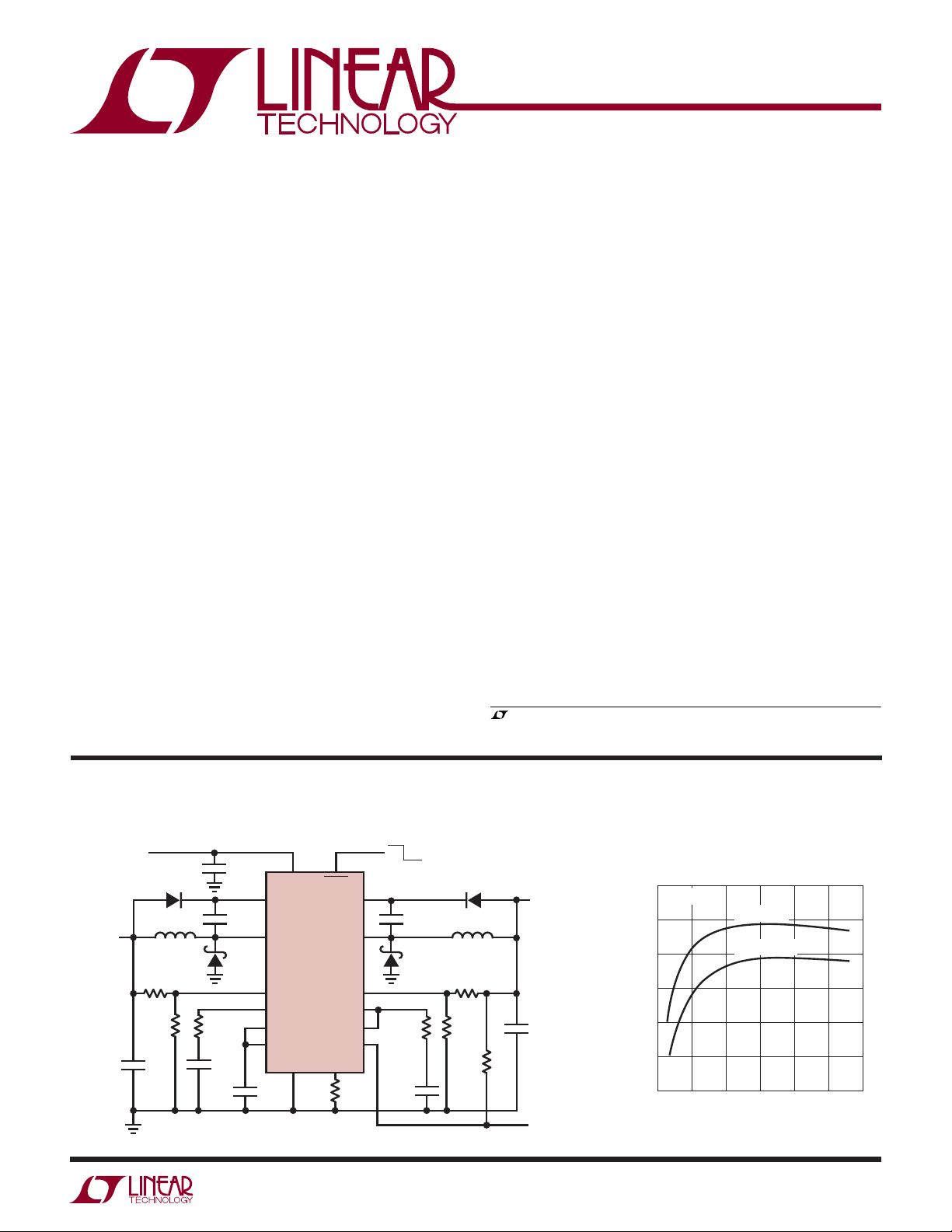
TYPICAL APPLICATION
3.3V and 5V Dual Output Step-Down Converter with Output Sequencing
V
5.6V TO 36V
OUT1
3.3V
1.4A
IN
35.7k
11.5k
22µF
6.8µH
4.7µF
0.22µF 0.22µF
51k
150pF
1nF
VINSHDN
BOOST1
SW1
LT3508
V
C1
TRACK/SS1
GND
f
= 700kHz
SW
BOOST2
SW2
RT/SYNC
FB2FB1
V
C2
PG1
PG2TRACK/SS2
52.3k
ON OFF
43k
100pF
10µH
56.2k
10.7k
100k
3508 TA01a
OUT2
5V
1.4A
10µF
POWER
GOOD
95
VIN = 12V
90
85
80
EFFICIENCY (%)
75
70
65
0
Effi ciency
V
= 5V
OUT2
V
= 3.3V
OUT1
0.5 1
LOAD CURRENT (A)
1.5
3508 TA01b
3508fb
1
LT3508
ABSOLUTE MAXIMUM RATINGS
VIN Pin Voltage ............................................(–0.3V), 40V
BOOST Pin Voltage ...................................................60V
BOOST Above SW Voltage ........................................30V
SHDN, PG Voltage .....................................................40V
TRACK/SS, FB, R
/SYNC, VC Voltage ..........................6V
T
Operating Junction Temperature Range (Note 2)
LT3508E ............................................. –40°C to 125°C
LT3508I .............................................. –40°C to 125°C
LT3508H ............................................ –40°C to 150°C
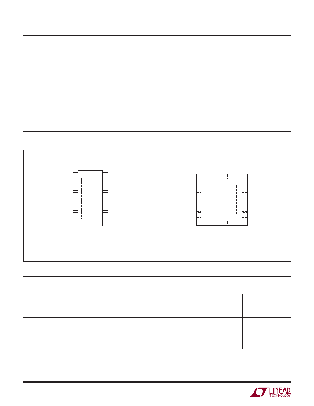
PIN CONFIGURATION
TOP VIEW
TRACK/SS1
BOOST1
BOOST2
TRACK/SS2
EXPOSED PAD (PIN 17) IS GND AND MUST BE SOLDERED TO PCB
1
2
3
SW1
4
V
IN1
V
IN2
SW2
16-LEAD PLASTIC TSSOP
θJA = 40°C/W, θJC = 10°C/W
5
6
7
8
FE PACKAGE
17
FB1
16
V
15
C1
PG1
14
R
/SYNC
13
T
SHDN
12
PG2
11
V
10
C2
FB2
9
(Note 1)
Storage Temperature Range
QFN .................................................... –65°C to 150°C
TSSOP ............................................... –65°C to 150°C
Lead Temperature (Soldering, 10 sec)
TSSOP .............................................................. 300°C
TOP VIEW
/SYNC
T
VC1PG1
R
24 23 22 21 20 19
1
FB1
TRACK/SS1
EXPOSED PAD (PIN 25) IS GND AND MUST BE SOLDERED TO PCB
2
3
GND
4
GND
5
GND
6
GND
24-LEAD (4mm s 4mm) PLASTIC QFN
25
7 8 9
BOOST1
θJA = 40°C/W, θJC = 10°C/W
10 11 12
IN1VIN2
V
SW1
UF PACKAGE
SHDN
PG2
SW2
C2
V
18
17
16
15
14
13
BOOST2
FB2
TRACK/SS2
GND
GND
GND
GND
ORDER INFORMATION
LEAD FREE FINISH TAPE AND REEL PART MARKING* PACKAGE DESCRIPTION TEMPERATURE RANGE
LT3508EFE#PBF LT3508EFE#TRPBF 3508FE 16-Lead Plastic TSSOP –40°C to 125°C
LT3508IFE#PBF LT3508IFE#TRPBF 3508FE 16-Lead Plastic TSSOP –40°C to 125°C
LT3508HFE#PBF LT3508HFE#TRPBF 3508HFE 16-Lead Plastic TSSOP –40°C to 150°C
LT3508EUF#PBF LT3508EUF#TRPBF 3508
LT3508IUF#PBF LT3508IUF#TRPBF 3508
LT3508HUF#PBF LT3508HUF#TRPBF 3508H
24-Lead (4mm × 4mm) Plastic QFN
24-Lead (4mm × 4mm) Plastic QFN
24-Lead (4mm × 4mm) Plastic QFN
–40°C to 125°C
–40°C to 125°C
–40°C to 150°C
Consult LTC Marketing for parts specifi ed with wider operating temperature ranges.*Temperature grades are identifi ed by a label on the shipping container.
Consult LTC Marketing for information on non-standard lead based fi nish parts.
For more information on lead free part marking, go to: http://www.linear.com/leadfree/
For more information on tape and reel specifi cations, go to: http://www.linear.com/tapeandreel/
3508fb
2
LT3508
ELECTRICAL CHARACTERISTICS
The l denotes the specifi cations which apply over the full operating
temperature range, otherwise specifi cations are at T
= 25°C. VIN = 12V, V
A
PARAMETER CONDITIONS MIN TYP MAX UNITS
Minimum Operating Voltage, V
Minimum Operating Voltage, V
Quiescent Current Not Switching 4.3 5.2 mA
V
IN1
Quiescent Current Not Switching 320 500 µA
V
IN2
Shutdown Current (V
IN1
IN1
V
IN2
+ V
)V
IN2
= 12V
IN1
= 0.3V 0.1 2 µA
SHDN
FB Voltage
FB Pin Bias Current (Note 3) V
= 0.800V, VC = 0.4V
FB
FB Voltage Line Regulation 5V < VIN < 40V 0.01 %/V
Error Amp Transconductance 300 µS
Error Amp Voltage Gain 600 V/V
to Switch Current Gain 2.5 A/V
V
C
Switching Frequency R
Switching Phase R
Maximum Duty Cycle (Note 4) R
Foldback Frequency R
= 33.2k
T
= 33.2k 150 180 210 Deg
T
= 33.2k
T
R
= 7.50k
T
R
= 169k
T
= 33.2k, VFB = 0V 120 kHz
T
Switch Current Limit (Note 5) Duty Cycle = 15%
Switch V
CESAT
ISW = 1.5A 300 mV
Switch Leakage Current 0.01 1 µA
Minimum Boost Voltage 1.7 2.5 V
Boost Pin Current I
TRACK/SS Pin Current V
PG Threshold Offset V
PG Voltage Output Low V
PG Pin Leakage V
= 1.5A 35 50 mA
SW
= 0V 0.8 1.2 2.2 µA
TRACK/SS
Rising 56 75 110 mV
FB
= 0.6V, IPG = 250µA 0.13 0.4 V
FB
= 2V 0.01 1 µA
PG
SHDN Threshold Voltage 2.53 2.63 2.73 V
SHDN Input Current (Note 6) V
= 60mV Above Threshold Voltage 6 8 10 µA
SHDN
SHDN Threshold Current Hysteresis 5.5 7.5 9.5 µA
SYNC Threshold Voltage 1 1.25 1.5 V
SYNC Input Frequency 0.25 2.5 MHz
= 17V unless otherwise noted. (Note 2)
BOOST
l
l
0.790
l
0.784
l
l
0.92 1 1.06 MHz
l
84 90
l
2.0 2.6 3.2 A
3.4 3.7 V
2.5 3.0 V
0.800 0.814
0.816
50 300 nA
80
98
%
%
%
V
V
Note 1: Stresses beyond those listed under Absolute Maximum Ratings
may cause permanent damage to the device. Exposure to any Absolute
Maximum Rating condition for extended periods may affect device
reliability and lifetime.
Note 2: The LT3508E is guaranteed to meet performance specifi cations
from 0°C to 125°C junction temperature. Specifi cations over the –40°C
to 125°C operating junction temperature range are assured by design,
characterization and correlation with statistical process controls. The
LT3508I is guaranteed over the full –40°C to 125°C operating junction
temperature range. The LT3508H is guaranteed over the full –40°C to
150°C operating junction temperature range. High junction temperatures
degrade operating lifetimes. Operating lifetime is derated at junction
temperatures greater than 125°C.
Note 3: Current fl ows out of pin.
Note 4: V
LT3508 when V
=12V. Circuitry increases the maximum duty cycle of the
BOOST
> VIN + 2.5V. See “Minimum Operating Voltage” in
BOOST
the Applications Information section for details.
Note 5: Current limit is guaranteed by design and/or correlation to static
test. Slope compensation reduces current limit at higher duty cycles.
Note 6: Current fl ows into pin.
Note 7: This IC includes overtemperature protection that is intended
to protect the device during momentary overload conditions. Junction
temperature will exceed the maximum operating junction temperature
range when overtemperature protection is active. Continuous operation
above the specifi ed maximum operating junction temperature may impair
device reliability.
3508fb
3
LT3508
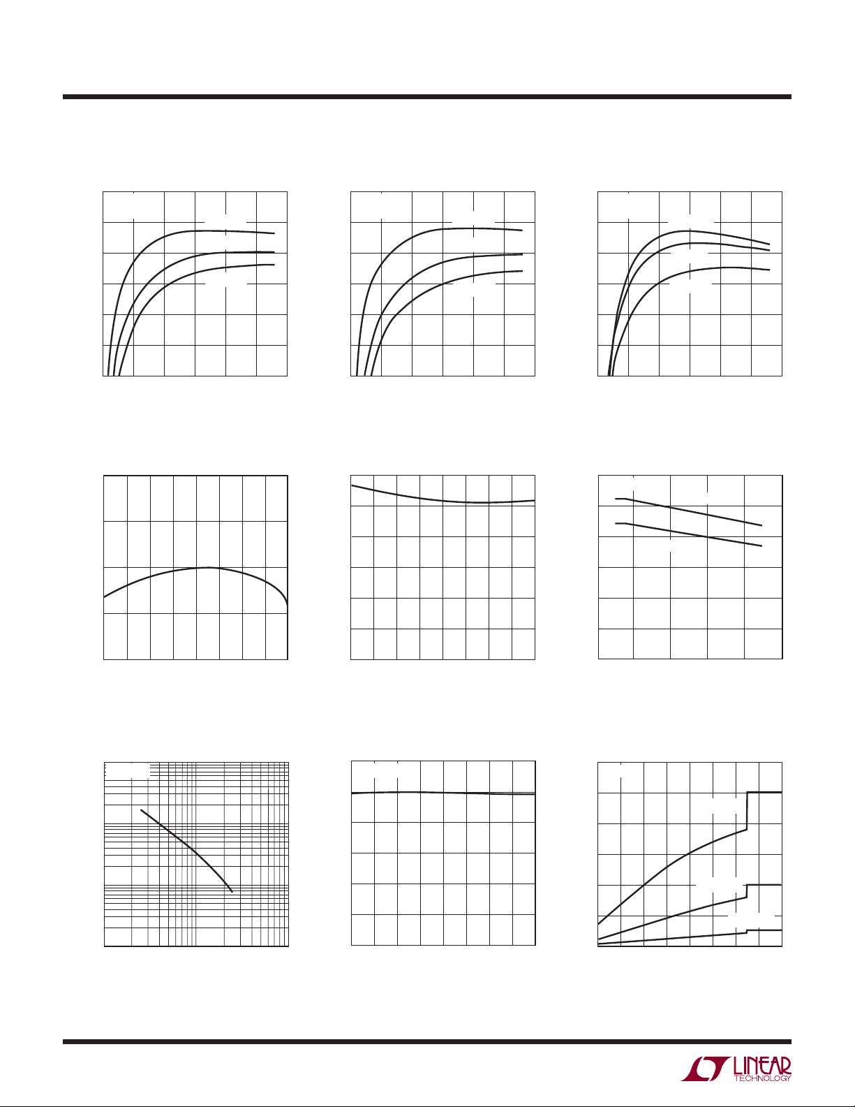
TYPICAL PERFORMANCE CHARACTERISTICS
Effi ciency, V
95
TA = 25°C
f = 700kHz
90
85
80
EFFICIENCY (%)
75
70
65
0
Feedback Voltage
0.810
0.805
0.800
= 5V
OUT
VIN = 12V
VIN = 24V
VIN = 32V
0.5 1
LOAD CURRENT (A)
3508 G01
1.5
Effi ciency, V
90
TA = 25°C
f = 700kHz
85
80
75
EFFICIENCY (%)
70
65
60
0
0.5 1
LOAD CURRENT (A)
Switch Current Limit
vs Temperature
3.0
2.5
2.0
1.5
= 3.3V Effi ciency, V
OUT
VIN = 12V
VIN = 24V
VIN = 32V
1.5
3508 G02
85
TA = 25°C
f = 1MHz
80
75
70
EFFICIENCY (%)
65
60
55
0
Switch Current Limit
vs Duty Cycle
3.0
TA = 25°C
2.5
2.0
1.5
= 1.8V
OUT
VIN = 3.3V
VIN = 5V
VIN = 12V
0.5 1
LOAD CURRENT (A)
TYPICAL
MINIMUM
1.5
3508 G03
FEEDBACK VOLTAGE (V)
0.795
0.790
–50
–25 0 25 50
TEMPERATURE (°C)
Switching Frequency vs R
1000
TA = 25°C
100
(k)
T
R
10
1
0.1
FREQUENCY (MHz)
1.0
CURRENT LIMIT (A)
0.5
0
75 100 125 150
3508 G04
–50 –25 0 25 50 75 100 125 150
Switching Frequency
T
110
3508 G07
vs Temperature
1.2
RT = 33.2k
1.0
0.8
0.6
0.4
SWITCHING FREQUENCY (MHz)
0.2
0
–50 –25 0 25 50 75 100 125 150
TEMPERATURE (°C)
TEMPERATURE (°C)
3508 G05
3508 G08
1.0
CURRENT LIMIT (A)
0.5
0
0
20 40 60 80
DUTY CYCLE (%)
Switching Frequency Foldback
3.0
TA = 25°C
2.5
2.0
1.5
1.0
SWITCHING FREQUENCY (MHz)
0.5
0
200 400 600 800
100 300 500 700
0
FEEDBACK VOLTAGE (mV)
RT = 7.50k
RT = 33.2k
100
3508 G06
RT = 169k
3508 G09
4
3508fb
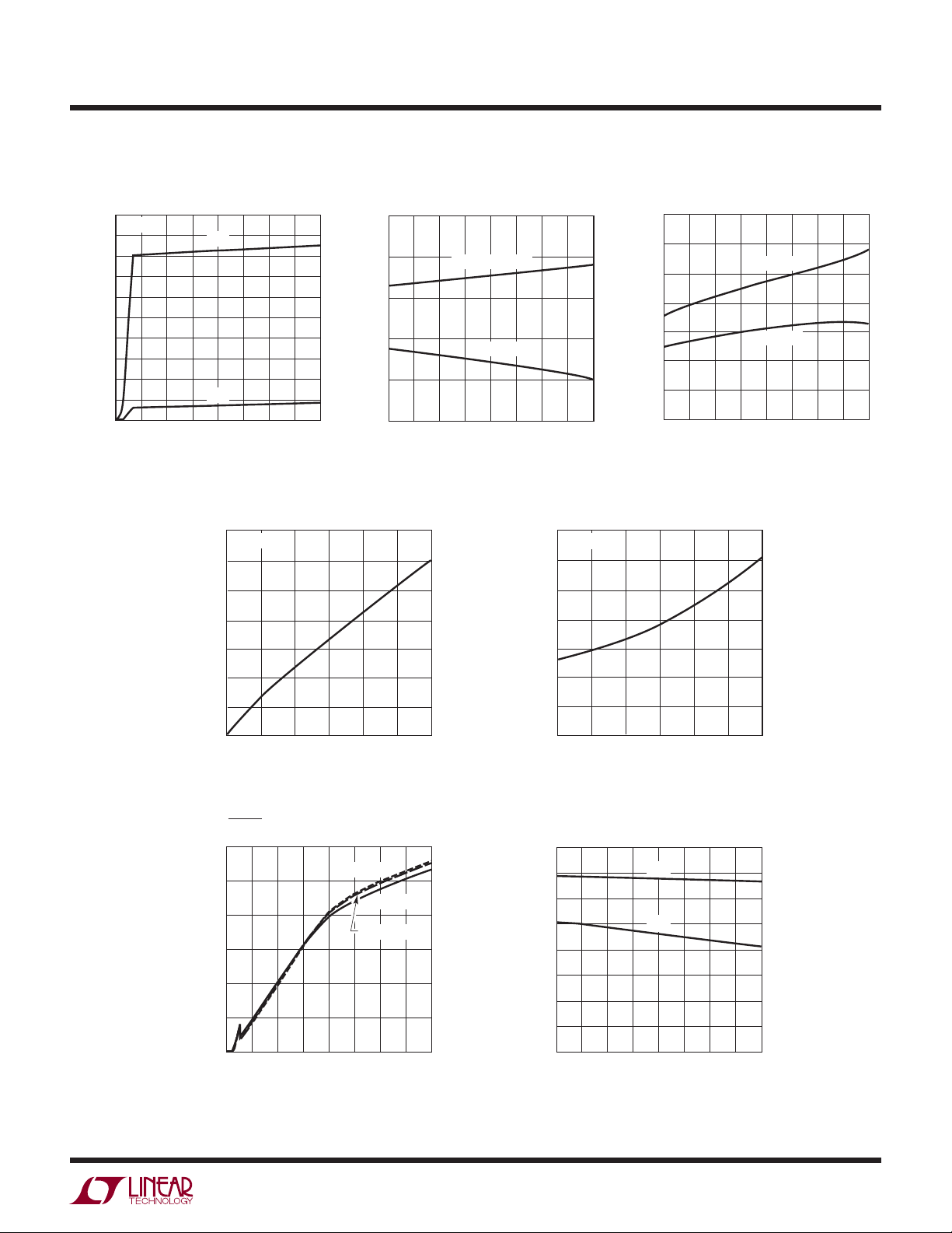
TYPICAL PERFORMANCE CHARACTERISTICS
LT3508
Quiescent Current VC Voltages
5.0
TA = 25°C
4.5
4.0
3.5
3.0
2.5
2.0
1.5
INPUT CURRENT (mA)
1.0
0.5
0
0
515
10
V
IN1
V
IN2
20
INPUT VOLTAGE (V)
25
35
30
40
3508 G10
2.5
2.0
1.5
VOLTAGE (V)
1.0
C
V
0.5
0
–50 –25 0 25 50 75 100 125 150
Switch Voltage Drop
350
TA = 25°C
300
250
200
150
CLAMP VOLTAGE
TO SWITCH
TEMPERATURE (°C)
3508 G11
Boost Pin Current
35
TA = 25°C
30
25
20
15
Error Amp Output Current
35
30
25
20
15
10
OUTPUT CURRENT (µA)
5
0
–50 –25 0 25 50 75 100 125 150
SINKING
SOURCING
TEMPERATURE (°C)
3508 G12
100
SWITCH VOLTAGE (mV)
50
0
0
SHDN Pin Current
120
100
80
60
40
SHDN PIN CURRENT (µA)
20
0
515
0
0.5
SWITCH CURRENT (A)
TA = –45°C
TA = 25°C
10 20
SHDN PIN VOLTAGE (V)
25
1 1.5
3508 G13
TA = 125°C
30
35
3508 G15
10
BOOST PIN CURRENT (mA)
5
0
0
0.5
SWITCH CURRENT (A)
1 1.5
3508 G14
Undervoltage Lockout
4.0
V
3.5
3.0
2.5
2.0
1.5
INPUT VOLTAGE (V)
1.0
0.5
40
0
–50 –25 0 25 50 75 100 125 150
IN1
V
IN2
TEMPERATURE (°C)
3508 G16
3508fb
5

LT3508
PIN FUNCTIONS
BOOST1, BOOST2: The BOOST pins are used to provide
drive voltages, higher than the input voltage, to the internal
NPN power switches. Tie through a diode to a 2.8V or
higher supply, such as V
OUT
or VIN.
Exposed Pad: The Exposed Pad metal of the package provides both electrical contact to ground and good thermal
contact to the printed circuit board. The Exposed Pad must
be soldered to the circuit board for proper operation.
FB1, FB2: The LT3508 regulates each feedback pin to
0.800V. Connect the feedback resistor divider taps to
these pins.
GND: Tie the GND pins directly to the Exposed Pad and
ground plane.
PG1, PG2: The power good pins are the open-collector
outputs of an internal comparator. PG remains low until
the FB pin is within 10% of the fi nal regulation voltage.
As well as indicating output regulation, the PG pins can
be used to sequence the two switching regulators. These
pins can be left unconnected. The PG outputs are valid
when V
is greater than 2.4V and SHDN is high. The PG
IN1
comparators are disabled in shutdown.
/SYNC: The RT/SYNC pin is used to set the internal
R
T
oscillator frequency. Tie a 33.2k resistor from R
/SYNC
T
to GND for a 1MHz switching frequency. To synchronize
the part to an external frequency, drive the R
/SYNC pin
T
with a logic-level signal with positive and negative pulse
widths of at least 80ns.
SHDN: The shutdown pin is used to put the LT3508 in
shutdown mode. Pull the pin below 0.3V to shut down the
LT3508. The 2.63V threshold can function as an accurate
undervoltage lockout (UVLO), preventing the regulator
from operating until the input voltage has reached the
programmed level. Do not drive SHDN more than 6V
above V
IN1
.
SW1, SW2: The SW pins are the outputs of the internal
power switches. Connect these pins to the inductors, catch
diodes and boost capacitors.
TRACK/SS1, TRACK/SS2: The TRACK/SS pins are used
to soft-start the two channels, to allow one channel to
track the other output, or to allow both channels to track
another output. For tracking, tie a resistor divider to this
pin from the tracked output. For soft-start, tie a capacitor
to this pin. An internal 1.2µA soft-start current charges
the capacitor to create a voltage ramp at the pin. Leave
these pins disconnected if unused.
, VC2: The VC pins are the outputs of the internal error
V
C1
amps. The voltages on these pins control the peak switch
currents. These pins are normally used to compensate the
control loops, but can also be used to override the loops.
Pull these pins to ground with an open drain to shut down
each switching regulator.
V
IN1
: The V
pin supplies current to the LT3508 internal
IN1
circuitry and to the internal power switch connected to
SW1 and must be locally bypassed. V
must be greater
IN1
than 3.7V for channel 1 or channel 2 to operate.
V
IN2
: The V
pin supplies current to the internal power
IN2
switch connected to SW2 and must be locally bypassed.
Connect this pin directly to V
nel 2 is coming from a different source. V
greater than 3V and V
must be greater than 3.7V for
IN1
unless power for chan-
IN1
must be
IN2
channel 2 to operate.
6
3508fb
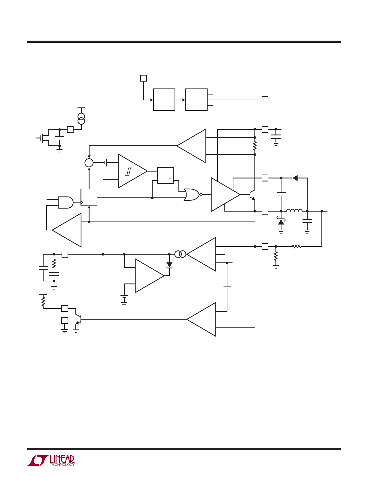
BLOCK DIAGRAM
SHDN
LT3508
V
IN1
RT/SYNC
V
IN
V
IN
C
IN
TRACK/SS
1.2µA
0.75V
INT REG
AND REF
MASTER
OSC
CLK1
CLK2
+
3
SLOPE
C1
SLAVE
CLK
OSC
+
0.625V
–
V
C
R
C
F
C
C
C
–
+
I
LIMIT
CLAMP
R
SQ
ERROR
AMP
–
+
+
TRACK/SS
+
75mV
0.80V
BOOST
SW
FB
D2
C3
L1
D1
C1
R1
R2
OUT
PG
+
GND
–
3508 F01
Figure 1. Block Diagram of the LT3508 with Associated External Components (One of Two Switching Regulators Shown)
3508fb
7

LT3508
OPERATION
The LT3508 is a dual constant frequency, current mode
regulator with internal power switches. Operation can be
best understood by referring to the Block Diagram. If the
SHDN pin is tied to ground, the LT3508 is shut down and
draws minimal current from the input source tied to the
pins. If the SHDN pin exceeds 1V, the internal bias
V
IN
circuits turn on, including the internal regulator, reference
and oscillator. The switching regulators will only begin to
operate when the SHDN pin exceeds 2.63V.
The switcher is a current mode regulator. Instead of directly
modulating the duty cycle of the power switch, the feedback
loop controls the peak current in the switch during each
cycle. Compared to voltage mode control, current mode
control improves loop dynamics and provides cycle-bycycle current limit. A pulse from the oscillator sets the
RS fl ip-fl op and turns on the internal NPN power switch.
Current in the switch and the external inductor begins to
increase. When this current exceeds a level determined
by the voltage at V
, current comparator C1 resets the
C
fl ip-fl op, turning off the switch. The current in the inductor
fl ows through the external Schottky diode and begins to
decrease. The cycle begins again at the next pulse from the
oscillator. In this way, the voltage on the V
pin controls
C
the current through the inductor to the output. The internal
error amplifi er regulates the output current by continually
adjusting the V
on the V
C
pin voltage. The threshold for switching
C
pin is 0.8V, and an active clamp of 1.75V limits
the output current.
The switching frequency is set either by the resistance to
GND at the R
signal driving the R
/SYNC pin or the frequency of the logic-level
T
/SYNC pin. A detection circuit monitors
T
for the presence of a SYNC signal on the pin and switches
between the two modes. Unique circuitry generates the
appropriate slope compensation ramps and generates the
180° out-of-phase clocks for the two channels.
The switching regulator performs frequency foldback
during overload conditions. An amplifi er senses when
is less than 0.625V and begins decreasing the oscil-
V
FB
lator frequency down from full frequency to 12% of the
nominal frequency when V
= 0V. The FB pin is less than
FB
0.8V during start-up, short-circuit and overload conditions.
Frequency foldback helps limit switch current under these
conditions.
The switch driver operates either from V
or from the
IN
BOOST pin. An external capacitor and Schottky diode
are used to generate a voltage at the BOOST pin that is
higher than the input supply. This allows the driver to
saturate the internal bipolar NPN power switch for effi cient operation.
The TRACK/SS pin serves as an alternative input to the
error amplifi er. The amplifi er will use the lowest voltage
of either the reference of 0.8V or the voltage on the
TRACK/SS pin as the positive input of error amplifi er.
Since the TRACK/SS pin is driven by a constant current
source, a single capacitor on the pin will generate a linear
ramp on the output voltage. Tying the TRACK/SS pin to a
resistor divider from the output of one of the switching
regulators allows one output to track another.
The PG output is an open-collector transistor that is off
when the output is in regulation, allowing an external
resistor to pull the PG pin high. Power good is valid when
the LT3508 is enabled (SHDN is high) and V
is greater
IN1
than ~2.4V.
8
3508fb

APPLICATIONS INFORMATION
LT3508
Setting the Output Voltage
The output voltage is programmed with a resistor divider
between the output and the FB pin. Choose the 1% resistors according to:
RR
12
⎛
⎜
⎝
OUT
08
.
⎞
1=
–
⎟
⎠
V
V
R2 should be 20k or less to avoid bias current errors.
Reference designators refer to the Block Diagram.
Minimum Operating Voltage
The minimum operating voltage is determined either by
the LT3508’s undervoltage lockout or by its maximum duty
cycle. If V
IN1
and V
are tied together, the undervoltage
IN2
lockout is at 3.7V or below. If the two inputs are used
separately, then V
or below and V
below. Because the internal supply runs off V
nel 2 will not operate unless V
has an undervoltage lockout of 3.7V
IN1
has an undervoltage lockout of 3V or
IN2
, chan-
IN1
> 3.7V. The duty cycle
IN1
is the fraction of time that the internal switch is on and is
determined by the input and output voltages:
VV
+
DC
OUT F
=
VV V
IN SW F
+–
where VF is the forward voltage drop of the catch diode
(~0.4V) and V
is the voltage drop of the internal switch
SW
(~0.4V at maximum load).
Example: I
= 1.5A/50mA = 30, DC
β
SW
V
IN MIN()
= 1.5A and I
SW
..
33 04
VV
96
+
–. . .=
%
= 50mA, V
BOOST
= 1/(1+1/30) = 96%:
MAX
+=
04 04 38
VVV
OUT
= 3.3V,
Maximum Operating Voltage
The maximum operating voltage is determined by the
Absolute Maximum Ratings of the V
and BOOST pins,
IN
and by the minimum duty cycle:
DC
MIN
where t
= t
ON(MIN)
ON(MIN)
• f
is equal to 130ns (for TJ > 125°C t
ON(MIN)
is equal to 150ns) and f is the switching frequency.
Running at a lower switching frequency allows a lower
minimum duty cycle. The maximum input voltage before
pulse skipping occurs depends on the output voltage and
the minimum duty cycle:
VV
+
V
IN PS
OUT F
DC
MIN
VV
–=
+
FSW()
Unlike many fi xed frequency regulators, the LT3508 can
extend its duty cycle by turning on for multiple cycles. The
LT3508 will not switch off at the end of each clock cycle if
there is suffi cient voltage across the boost capacitor (C3
in Figure 1). Eventually, the voltage on the boost capacitor
falls and requires refreshing. Circuitry detects this condition and forces the switch to turn off, allowing the inductor
current to charge up the boost capacitor. This places a
limitation on the maximum duty cycle as follows:
DC
MAX
=
1
+11
β
SW
where βSW is equal to the SW pin current divided by the
BOOST pin current as shown in the Typical Performance
Characteristics section. This leads to a minimum input
voltage of:
VV
+
V
IN MIN
OUT F
DC
MAX
VV
–=
+
FSW()
Example: f = 790kHz, V
= 3.3V, DC
OUT
= 130ns • 790kHz
MIN
= 0.103:
..
+
33 04
V
IN PS()
VV
.
0 103
–. .=
+=
04 04 36
VVV
The LT3508 will regulate the output current at input voltages
greater than V
. For example, an application with an
IN(PS)
output voltage of 1.8V and switching frequency of 1.5MHz
has a V
of 11.3V, as shown in Figure 2. Figure 3 shows
IN(PS)
operation at 18V. Output ripple and peak inductor current
have signifi cantly increased. Exceeding V
IN(PS)
is safe if
the output is in regulation, if the external components have
adequate ratings to handle the peak conditions and if the
peak inductor current does not exceed 3.2A. A saturating
inductor may further reduce performance. Do not exceed
V
greater than 5V, use V
during start-up or overload conditions (for outputs
IN(PS)
= 5V to calculate V
OUT
IN(PS)
). For
operation above 20V in pulse skipping mode, program
the switching frequency to 1.1MHz or less.
3508fb
9

LT3508
APPLICATIONS INFORMATION
V
OUT
100mV/DIV
(AC)
I
L
500mA/DIV
3508 F02
= 1.8V and
OUT
Figure 2. Operation Below V
2µs/DIV
. VIN = 10V, V
IN(PS)
fSW = 1.5MHz
V
OUT
100mV/DIV
(AC)
I
L
500mA/DIV
2µs/DIV
Figure 3. Operation Above V
. VIN = 18V, V
IN(PS)
3508 F03
OUT
= 1.8V
and fSW = 1.5MHz. Output Ripple and Peak Inductor Current
Increase
Table 1. Programming the Switching Frequency
SWITCHING FREQUENCY (MHz)
2.5 7.50
2.2 9.76
2 11.5
1.8 14
1.6 16.9
1.4 20.5
1.2 26.1
1 33.2
0.9 38.3
0.8 44.2
0.7 52.3
0.6 61.9
0.5 76.8
0.45 88.7
0.4 100
0.35 115
0.3 140
0.25 169
R
(kΩ)
T
Setting the Switching Frequency
The switching frequency is programmed either by driving
/SYNC pin with a logic level SYNC signal or by tying
the R
T
a resistor from the R
selecting the value of R
/SYNC pin to ground. A graph for
T
for a given operating frequency
T
is shown in the Typical Application section. Suggested
programming resistors for various switching frequencies
are shown in Table 1.
Choosing a high switching frequency will allow the smallest
overall solution size. However, at high input voltages the
effi ciency can drop signifi cantly with increasing switching
frequency. The choice of switching frequency will also
impact the input voltage range, inductor and capacitor
selection, and compensation. See the related sections
for details.
Inductor Selection and Maximum Output Current
A good fi rst choice for the inductor value is:
MHz
LV V
=+
()
OUT F
.12
•
f
where VF is the voltage drop of the catch diode (~0.4V) and L
is in H. The inductor’s RMS current rating must be greater
than the maximum load current and its saturation current
should be at least 30% higher. For highest effi ciency, the
series resistance (DCR) should be less than 0.1Ω. Table 2
lists several vendors and types that are suitable.
Table 2. Inductor Vendors
VENDOR URL PART SERIES TYPE
Coilcraft www.coilcraft MSS7341 Shielded
Murata www.murata.com LQH55D Open
TDK www.component.tdk.com SLF7045
SLF10145
Toko www.toko.com DC62CB
D63CB
D75C
D75F
Sumida www.sumida.com CR54
CDRH74
CDRH6D38
CR75
Shielded
Shielded
Shielded
Shielded
Shielded
Open
Open
Shielded
Shielded
Open
3508fb
10

APPLICATIONS INFORMATION
LT3508
The optimum inductor for a given application may differ
from the one indicated by this simple design guide. A larger
value inductor provides a higher maximum load current,
and reduces the output voltage ripple. If your load is lower
than the maximum load current, then you can relax the
value of the inductor and operate with higher ripple current. This allows you to use a physically smaller inductor,
or one with a lower DCR resulting in higher effi ciency.
Be aware that if the inductance differs from the simple
rule above, then the maximum load current will depend
on input voltage. In addition, low inductance may result
in discontinuous mode operation, which further reduces
maximum load current. For details of maximum output
current and discontinuous mode operation, see Linear
Technology’s Application Note 44. Finally, for duty cycles
greater than 50% (V
OUT/VIN
> 0.5), a minimum inductance
is required to avoid sub-harmonic oscillations:
kHz
LVV
=+
()
MIN OUT F
•
800
f
The current in the inductor is a triangle wave with an average
value equal to the load current. The peak switch current
is equal to the output current plus half the peak-to-peak
inductor ripple current. The LT3508 limits its switch current in order to protect itself and the system from overload
faults. Therefore, the maximum output current that the
LT3508 will deliver depends on the switch current limit,
the inductor value, and the input and output voltages.
When the switch is off, the potential across the inductor
is the output voltage plus the catch diode drop. This gives
the peak-to-peak ripple current in the inductor:
1–
DC V V
()
ΔI
=
L
+
()
OUT F
•
Lf
where f is the switching frequency of the LT3508 and L
is the value of the inductor. The peak inductor and switch
current is:
I
Δ
III
SW PK L PK OUT
==+
() ()
L
2
To maintain output regulation, this peak current must be
. I
less than the LT3508’s switch current limit I
LIM
LIM
is
at least 2A for at low duty cycles and decreases linearly
to 1.55A at DC = 90%. The maximum output current is a
function of the chosen inductor value:
ΔΔ
IIIADC
OUT MAX LIM
()
LL
–•–.•–==
21025
()
2
I
2
Choosing an inductor value so that the ripple current is
small will allow a maximum output current near the switch
current limit.
One approach to choosing the inductor is to start with the
simple rule given above, look at the available inductors, and
choose one to meet cost or space goals. Then use these
equations to check that the LT3508 will be able to deliver
the required output current. Note again that these equations
assume that the inductor current is continuous. Discontinuous operation occurs when I
is less than ΔIL/2.
OUT
Input Capacitor Selection
Bypass the V
pins of the LT3508 circuit with a ceramic
IN
capacitor of X7R or X5R type. For switching frequencies
above 500kHz, use a 4.7µF capacitor or greater. For switching frequencies below 500kHz, use a 10µF or higher capacitor. If the V
is necessary. If the V
pins are tied together only a single capacitor
IN
pins are separated, each pin will
IN
need its own bypass. The following paragraphs describe
the input capacitor considerations in more detail.
Step-down regulators draw current from the input supply
in pulses with very fast rise and fall times. The input capacitor is required to reduce the resulting voltage ripple at
the LT3508 input and to force this switching current into a
tight local loop, minimizing EMI. The input capacitor must
have low impedance at the switching frequency to do this
effectively, and it must have an adequate ripple current
rating. With two switchers operating at the same frequency
but with different phases and duty cycles, calculating the
input capacitor RMS current is not simple. However, a
conservative value is the RMS input current for the channel
that is delivering most power (V
VVV
()
CI
IN RMS OUT
=
()
and is largest when VIN = 2V
OUT IN OUT
•
V
IN
OUT
times I
OUT
–
(50% duty cycle). As
<
OUT
I
OUT
):
2
the second, lower power channel draws input current,
3508fb
11

LT3508
APPLICATIONS INFORMATION
the input capacitor’s RMS current actually decreases as
the out-of-phase current cancels the current drawn by
the higher power channel. Considering that the maximum
load current from a single channel is ~1.4A, RMS ripple
current will always be less than 0.7A.
The high frequency of the LT3508 reduces the energy storage requirements of the input capacitor. The combination
of small size and low impedance (low equivalent series
resistance or ESR) of ceramic capacitors makes them the
preferred choice. The low ESR results in very low voltage
ripple. Ceramic capacitors can handle larger magnitudes
of ripple current than other capacitor types of the same
value. Use X5R and X7R types.
An alternative to a high value ceramic capacitor is a lower
value ceramic along with a larger electrolytic capacitor. The
electrolytic capacitor likely needs to be greater than 10µF
in order to meet the ESR and ripple current requirements.
The input capacitor is likely to see high surge currents
when the input source is applied. Tantalum capacitors
can fail due to an oversurge of current. Only use tantalum
capacitors with the appropriate surge current rating. The
manufacturer may also recommend operation below the
rated voltage of the capacitor.
A fi nal caution is in order regarding the use of ceramic
capacitors at the input. A ceramic input capacitor can
combine with stray inductance to form a resonant tank
circuit. If power is applied quickly (for example by plugging
the circuit into a live power source), this tank can ring,
doubling the input voltage and damaging the LT3508. The
solution is to either clamp the input voltage or dampen the
tank circuit by adding a lossy capacitor in parallel with the
ceramic capacitor. For details see Application Note 88.
Output Capacitor Selection
The output capacitor has two essential functions. Along
with the inductor, it fi lters the square wave generated by the
LT3508 to produce the DC output. In this role it determines
the output ripple, and low impedance at the switching
frequency is important. The second function is to store
energy in order to satisfy transient loads and stabilize the
LT3508’s control loop. Ceramic capacitors have very low
equivalent series resistance (ESR) and provide the best
ripple performance. A good value is:
VVMHz
C
OUT
where C
50 1
=
OUT
•
OUT
f
is in µF. Use X5R or X7R types. This choice
will provide low output ripple and good transient response.
Transient performance can be improved with a high value
capacitor if the compensation network is also adjusted to
maintain the loop bandwidth. A lower value of output capacitor can be used, but transient performance will suffer. With
an external compensation network, the loop gain can be
lowered to compensate for the lower capacitor value. Look
carefully at the capacitor’s data sheet to fi nd out what the
actual capacitance is under operating conditions (applied
voltage and temperature). A physically larger capacitor, or
one with a higher voltage rating, may be required. High
performance electrolytic capacitors can be used for the
output capacitor. Low ESR is important, so choose one
that is intended for use in switching regulators. The ESR
should be specifi ed by the supplier, and should be 0.05Ω
or less. Such a capacitor will be larger than a ceramic
capacitor and will have a larger capacitance, because the
capacitor must be large to achieve low ESR. Table 3 lists
several capacitor vendors.
Table 3. Capacitor Vendors
VENDOR PART SERIES COMMENTS
Panasonic Ceramic
Kemet Ceramic
Sanyo Ceramic
Murata Ceramic
AVX Ceramic
Taiyo Yuden Ceramic
TDK Ceramic
Polymer
Tantalum
Tantalum T494, T495
Polymer
Tantalum
Tantalum TPS Series
EEF Series
POSCAP
12
3508fb

APPLICATIONS INFORMATION
LT3508
Diode Selection
The catch diode (D1 from Figure 1) conducts current only
during switch off time. Average forward current in normal
operation can be calculated from:
–
()
V
IN
I
D AVG
()
IVV
OUT IN OUT
=
The only reason to consider a diode with a larger current
rating than necessary for nominal operation is for the
worst-case condition of shorted output. The diode current
will then increase to the typical peak switch current.
Peak reverse voltage is equal to the regulator input voltage.
Use a diode with a reverse voltage rating greater than the
input voltage. Table 4 lists several Schottky diodes and their
manufacturers. If operating at high ambient temperatures,
consider using a Schottky with low reverse leakage.
Table 4. Schottky Diodes
at 1A
V
PART NUMBER
On Semiconductor
MBR0520L 20 0.5
MBR0540 40 0.5 620
MBRM120E 20 1 530
MBRM140 40 1 550
Diodes Inc.
B0530W 30 0.5
B120 20 1 500
B130 30 1 500
B140HB 40 1
DFLS140 40 1.1 510
B240 40 2 500
R
(V)
I
AVE
(A)
V
F
(mV)
VF at 2A
(mV)
BOOST Pin Considerations
The capacitor and diode tied to the BOOST pin generate
a voltage that is higher than the input voltage. In most
cases, a 0.22µF capacitor and fast switching diode (such
as the CMDSH-3 or MMSD914LT1) will work well. For
applications 1MHz or faster, a 0.1µF capacitor is suffi cient.
Use a 0.47µF capacitor or greater for applicaitons running
below 500kHz. Figure 4 shows three ways to arrange the
boost circuit. The BOOST pin must be more than 2.5V
above the SW pin for full effi ciency. For outputs of 3.3V
and higher, the standard circuit (Figure 4a) is best. For
outputs between 2.8V and 3.3V, use a small Schottky diode
(such as the BAT-54). For lower output voltages, the boost
diode can be tied to the input (Figure 4b). The circuit in
Figure 4a is more effi cient because the boost pin current
comes from a lower voltage source. Finally, the anode of
the boost diode can be tied to another source that is at
least 3V (Figure 4c). For example, if you are generating
a 3.3V output, and the 3.3V output is on whenever the
particular channel is on, the anode of the BOOST diode
can be connected to the 3.3V output. In any case, be sure
that the maximum voltage at the BOOST pin is both less
than 60V and the voltage difference between the BOOST
and SW pins is less than 30V.
D2
BOOST
V
IN
V
BOOST
MAX V
V
IN
V
BOOST
MAX V
V
> 3V
IN2
V
IN
V
BOOST
MAX V
MINIMUM VALUE FOR V
LT3508
V
IN
GND
– VSW V
VIN + V
BOOST
D2
BOOST
LT3508
V
IN
GND
– VSW V
2V
BOOST
D2
BOOST
LT3508
V
IN
GND
– VSW V
V
BOOST
IN2
OUT
IN
IN
IN2
+ V
SW
OUT
(4a)
SW
(4b)
SW
IN
IN2
(4c)
Figure 4. Generating the Boost Voltage
C3
V
OUT
C3
V
OUT
C3
V
OUT
3508 F04
3V
=
3508fb
13

LT3508
APPLICATIONS INFORMATION
The minimum operating voltage of an LT3508 application
is limited by the undervoltage lockout (≈3.7V) and by the
maximum duty cycle. The boost circuit also limits the
minimum input voltage for proper start-up. If the input
voltage ramps slowly, or the LT3508 turns on when the
output is already in regulation, the boost capacitor may
not be fully charged. Because the boost capacitor charges
with the energy stored in the inductor, the circuit will rely
on some minimum load current to get the boost circuit
running properly. This minimum load will depend on
input and output voltages, and on the arrangement of the
boost circuit. The minimum load current generally goes
to zero once the circuit has started. Figure 5 shows a plot
of minimum load to start and to run as a function of input
voltage. Even without an output load current, in many
Minimum Input Voltage, V
6.5
TA = 25°C
= 3.3V
V
OUT
6.0
5.5
5.0
4.5
INPUT VOLTAGE (V)
4.0
3.5
3.0
INPUT VOLTAGE (V)
Figure 5. The Minimum Input Voltage Depends on Output
Voltage, Load Current and Boost Circuit
TO RUN
10 100 10000
1
Minimum Input Voltage, V
9
TA = 25°C
= 5V
V
OUT
8
7
6
TO RUN
5
4
1
10
TO START
LOAD CURRENT (mA)
TO START
100
LOAD CURRENT (mA)
OUT
1000
1000
= 3.3V
OUT
3508 F05a
= 5V
10000
3508 G05b
cases the discharged output capacitor will present a load
to the switcher that will allow it to start. The plots show
the worst case, where V
is ramping very slowly.
IN
Frequency Compensation
The LT3508 uses current mode control to regulate the
output. This simplifi es loop compensation. In particular, the
LT3508 does not require the ESR of the output capacitor
for stability, so you are free to use ceramic capacitors to
achieve low output ripple and small circuit size.
Frequency compensation is provided by the components
tied to the V
) and a resistor (RC) in series to ground are used. In
(C
C
pin, as shown in Figure 1. Generally a capacitor
C
addition, there may be a lower value capacitor in parallel.
This capacitor (C
) is not part of the loop compensation
F
but is used to fi lter noise at the switching frequency, and
is required only if a phase-lead capacitor is used or if the
output capacitor has high ESR.
Loop compensation determines the stability and transient
performance. Designing the compensation network is a bit
complicated and the best values depend on the application
and in particular the type of output capacitor. A practical
approach is to start with one of the circuits in this data
sheet that is similar to your application and tune the compensation network to optimize the performance. Stability
should then be checked across all operating conditions,
including load current, input voltage and temperature. The
LT1375 data sheet contains a more thorough discussion of
loop compensation and describes how to test the stability
using a transient load.
Figure 6 shows an equivalent circuit for the LT3508 control
loop. The error amplifi er is a transconductance amplifi er
with fi nite output impedance. The power section, consisting
of the modulator, power switch and inductor, is modeled
as a transconductance amplifi er generating an output
current proportional to the voltage at the V
pin. Note that
C
the output capacitor integrates this current, and that the
capacitor on the V
pin (CC) integrates the error amplifi er
C
output current, resulting in two poles in the loop. In most
cases a zero is required and comes from either the output
capacitor ESR or from a resistor R
in series with CC.
C
This simple model works well as long as the value of the
inductor is not too high and the loop crossover frequency
3508fb
14

APPLICATIONS INFORMATION
LT3508
is much lower than the switching frequency. A phase-lead
capacitor (C
) across the feedback divider may improve
PL
the transient response.
LT3508
CURRENT MODE
POWER STAGE
g
= 2.5S
m
V
GND
R
AMPLIFIER
g
m
300µS
2M
C
C
C
C
F
C
Figure 6. Model for Loop Response
ERROR
=
V
SW
R1
FB
–
+
0.8V
R2
POLYMER
TANTALUM
OUTPUT
C
PL
ESR
C1
OR
C1
+
CERAMIC
3508 F06
Shutdown and Undervoltage Lockout
Figure 7 shows how to add undervoltage lockout (UVLO)
to the LT3508. Typically, UVLO is used in situations where
the input supply is current limited, or has a relatively high
source resistance. A switching regulator draws constant
power from the source, so source current increases as
source voltage drops. This looks like a negative resistance
load to the source and can cause the source to current
limit or latch low under low source voltage conditions.
UVLO prevents the regulator from operating at source
voltages where the problems might occur.
An internal comparator will force the part into shutdown
below the minimum V
of 3.7V. This feature can be
IN1
used to prevent excessive discharge of battery-operated
systems.
If an adjustable UVLO threshold is required, the SHDN
pin can be used. The threshold voltage of the SHDN pin
comparator is 2.63V. Current hysteresis is added above the
SHDN threshold. This can be used to set voltage hysteresis
of the UVLO using the following:
VV
–
R
R
HL
3
=
μA
75
.
263
4
=
VV
–.
H
263
R
3
.
V
μA
8
–
Example: switching should not start until the input is above
4.75V and is to stop if the input falls below 4V.
VVVV
==
475 40
., .
HL
VV
475 4
R
R
.–
==
3
=
4
μA
75
.
.
663
2
475 263
VV
.–.
100
k
V
100
–
k
8
μA
=
200
k
Keep the connection from the resistor to the SHDN pin
short and make sure the interplane or surface capacitance
to switching nodes is minimized. If high resistor values are
used, the SHDN pin should be bypassed with a 1nF capacitor
to prevent coupling problems from the switch node.
Soft-Start
LT3508
V
IN
R3
SHDN
R4C1
2.6V
–
+
V
TRACK/SS
C
The output of the LT3508 regulates to the lowest voltage
present at either the TRACK/SS pin or an internal 0.8V
reference. A capacitor from the TRACK/SS pin to ground
is charged by an internal 1.2A current source resulting
in a linear output ramp from 0V to the regulated output
whose duration is given by:
8µA
7.5µA
Figure 7. Undervoltage Lockout
3508 F07
t
RAMP
At power up, internal open-collector ouputs discharge
both TRACK/SS pins. The pins clamp at 1.3V.
CV
•..08
SS
=
12
μA
3508fb
15

LT3508
APPLICATIONS INFORMATION
Output Tracking and Sequencing
Complex output tracking and sequencing between channels
can be implemented using the LT3508’s TRACK/SS and
PG pins. Figure 8 shows several confi gurations for output
tracking and sequencing of 5V and 3.3V applications.
Independent Start-Up Ratiometric Start-Up
V
OUT1
V
1V/DIV
0.1µF
0.047µF
20ms/DIV
TRACK/SS1
LT3508
TRACK/SS2
(8a)
V
V
OUT1
OUT2
OUT2
5V
3.3V
1V/DIV
20ms/DIV
TRACK/SS1
0.22µF
TRACK/SS2
Independent soft-start for each channel is shown in
Figure 8a. The output ramp time for each channel is set
by the soft-start capacitor as described in the soft-start
section.
Coincident Start-Up
LT3508
(8b)
V
V
OUT1
OUT2
V
V
OUT1
OUT2
5V
3.3V
1V/DIV
0.1µF
TRACK/SS1
TRACK/SS2
R2
10.0k
20ms/DIV
V
LT3508
V
R1
28.7k
OUT1
OUT2
(8c)
V
V
OUT1
OUT2
5V
3.3V
1V/DIV
0.1µF
0.047µF
Output Sequencing
20ms/DIV
TRACK/SS1
TRACK/SS2
LT3508
V
V
OUT1
PG1
OUT2
(8d)
V
V
OUT1
OUT2
5V
3.3V
Figure 8
1V/DIV
EXTERNAL
Controlled Power Up and Down
V
OUT1
V
OUT2
EXTERNAL SOURCE
20ms/DIV
SOURCE
+
–
TRACK/SS1
TRACK/SS2
R2
10.0k
V
LT3508
V
R1
28.7k
OUT1
OUT2
(8e)
5V
3.3V
3508fb
16

APPLICATIONS INFORMATION
LT3508
Ratiometric tracking is achieved in Figure 8b by connecting
both the TRACK/SS pins together. In this confi guration the
TRACK/SS pin source current is doubled (2.4A) which
must be taken into account when calculating the output
rise time.
By connecting a feedback network from V
TRACK/SS2 pin with the same ratio that set the V
OUT1
to the
OUT2
voltage, absolute tracking shown in Figure 8c is implemented. A small V
voltage offset will be present due
OUT2
to the TRACK/SS2 1.2A source current. This offset can
be corrected for by slightly reducing the value of R2. Use
a resistor divider such that when V
is in regulation,
OUT1
TRACK/SS2 is pulled up to 1V or greater. If TRACK/SS is
below 1V, the output may regulate FB to a voltage lower
than the 800mV reference voltage.
Figure 8d illustrates output sequencing. When V
OUT1
is within 10% of its regulated voltage, PG1 releases
the TRACK/SS2 soft-start pin allowing V
OUT2
to softstart. In this case PG1 will be pulled up to 1.3V by the
TRACK/SS pin.
If precise output ramp up and down is required, drive the
TRACK/SS pins as shown in Figure 8e.
Multiple Inputs
For applications requiring large inductors due to high V
to V
ratios, a 2-stage step down approach may reduce
OUT
IN
inductor size by allowing an increase in frequency. A dual
step-down application (Figure 9) steps down the input
voltage (V
voltage to power the second output (V
) to the highest output voltage, then uses that
IN1
IN2
). V
OUT1
must be
able to provide enough current for its output plus the input
current at V
when V
IN2
is at its maximum load.
OUT2
For applications with multiple input voltages, the LT3508
can accommodate input voltages as low as 3V on V
IN2
.
This can be useful in applications regulating outputs from
a PCI Express bus, where the 12V input is power limited
and the 3.3V input has power available to drive other
outputs. In this case, tie the 12V input to V
3.3V input to V
. See the Typical Application section for
IN2
and the
IN1
an example circuit.
Do not tie TRACK/SS1 and TRACK/SS2 together if using
multiple inputs. If V
is below 3V, TRACK/SS2 pulls low
IN2
and would hold TRACK/SS1 low as well if the two pins
are tied together, which would prevent channel 1 from
operating.
Shorted and Reverse Input Protection
If the inductor is chosen so that it won’t saturate excessively, an LT3508 step-down regulator will tolerate a shorted
output. There is another situation to consider in systems
where the output will be held high when the input to the
LT3508 is absent. This may occur in battery charging
OUT1
5V
0.9A
V
5.7V TO 36V
L1 6.8µH
R1
56.2k
R3
10.7k
C4
10µF
IN
D1
R5
39k
C1
4.7µF
ON OFF
C2
0.1µF
D3 D4
C6
100pF
C8
1nF
V
IN1VIN2
SHDN
BOOST1
SW1
V
C1
TRACK/SS1
GND
C9
3.3nF
f
SW
LT3508
RT/SYNC
= 1MHz
BOOST2
SW2
FB2FB1
V
PG1
PG2TRACK/SS2
R8
33.2k
C2
330pF
D2
47k
C7
C3
0.1µF
R6
OUT1
3.3µH
R2
18.7k
R4
15.0k
Figure 9. 1MHz, Wide Input Range 5V and 1.8V Outputs
L2
OUT2
1.8V
1A
C5
47µF
R7
100k
POWER
3508 F09
GOOD
3508fb
17

LT3508
APPLICATIONS INFORMATION
applications or in battery back-up systems where a battery
or some other supply is diode OR-ed with the LT3508’s
output. If the V
pin is allowed to fl oat and the SHDN pin
IN
is held high (either by a logic signal or because it is tied
), then the LT3508’s internal circuitry will pull its
to V
IN
quiescent current through its SW pin. This is fi ne if your
system can tolerate a few mA in this state. If you ground
the SHDN pin, the SW pin current will drop to essentially
zero. However, if the V
pin is grounded while the output
IN
is held high, then parasitic diodes inside the LT3508 can
pull large currents from the output through the SW pin
and the V
pin. Figure 10 shows a circuit that will run
IN
only when the input voltage is present and that protects
against a shorted or reversed input.
PARASITIC DIODE
D4
V
IN
V
IN
LT3508
SW
3508 F10
V
OUT
PCB Layout
For proper operation and minimum EMI, care must be taken
during printed circuit board layout. Figure 11 shows the
recommended PCB layout with trace and via locations. Note
that large, switched currents fl ow in the LT3508’s V
SW pins, the catch diode (D1) and the input capacitor (C
IN
and
).
IN
The loop formed by these components should be as small
as possible. These components, along with the inductor
and output capacitor, should be placed on the same side
of the circuit board, and their connections should be made
on that layer. Place a local, unbroken ground plane below
these components. The SW and BOOST nodes should be
as small as possible. Finally, keep the FB and V
nodes
C
small so that the ground traces will shield them from the
SW and BOOST nodes. The Exposed Pad on the bottom of
the package must be soldered to ground so that the pad
acts as a heat sink. To keep thermal resistance low, extend
the ground plane as much as possible, and add thermal
vias under and near the LT3508 to additional ground planes
within the circuit board and on the bottom side.
Figure 10. Diode D4 Prevents a Shorted Input from Discharging
a Backup Battery Tied to the Output
(11a) Example Layout for FE16 Package (11b) Example Layout for QFN Package
Figure 11. A Good PCB Layout Ensures Proper Low EMI Operation
18
3508fb

APPLICATIONS INFORMATION
LT3508
High Temperature Considerations
The die temperature of the LT3508 must be lower than the
maximum rating of 125°C (150°C for the H grade). This is
generally not a concern unless the ambient temperature is
above 85°C. For higher temperatures, care should be taken
in the layout of the circuit to ensure good heat sinking of
the LT3508. The maximum load current should be derated
as the ambient temperature approaches 125°C (150°C
for the H grade). The die temperature is calculated by
multiplying the LT3508 power dissipation by the thermal
resistance from junction to ambient. Power dissipation
within the LT3508 can be estimated by calculating the total
power loss from an effi ciency measurement and subtracting the catch diode loss. Thermal resistance depends on
the layout of the circuit board, but values from 30°C/W to
60°C/W are typical. Die temperature rise was measured
on a 4-layer, 6.5cm × 7.5cm circuit board in still air at a
load current of 1.4A (f
= 700kHz). For a 12V input to
SW
3.3V output the die temperature elevation above ambient
was 13°C; for 24VIN to 3.3V
12V
IN
to 5V
the rise was 14°C and for 24VIN to 5V
OUT
the rise was 18°C; for
OUT
OUT
the rise was 19°C.
Outputs Greater Than 6V
For outputs greater than 6V, add a resistor of 1k to 2.5k
across the inductor to damp the discontinuous ringing of
the SW node, preventing unintended SW current. The 12V
output circuit in the Typical Applications section shows
the location of this resistor.
Other Linear Technology Publications
Application Notes 19, 35 and 44 contain more detailed
descriptions and design information for step-down regulators and other switching regulators. The LT1376 data
sheet has a more extensive discussion of output ripple,
loop compensation and stability testing. Design Note 318
shows how to generate a dual polarity output supply using
a step-down regulator.
TYPICAL APPLICATIONS
V
IN
3.9V TO 16V
OUT2
OUT1
1.8V
1.4A
L1 3.3µH
R1
18.7k
R3
15.0k
C4
47µF
C1 TO C5: X5R OR X7R
D1, D2: MMSD4148
D3: DIODES INC. B140
D4: DIODES INC. B240A
1MHz, 3.3V and 1.8V Outputs with Sequencing
FB2FB1
V
C2
PG1
PG2TRACK/SS2
R8
33.2k
ON OFF
C3
0.1µF
R6
39k
C7
150pF
C1
D1
4.7µF
C2
0.1µF
D3 D4
R5
47k
C6
330pF
C8
1nF
V
V
IN1
BOOST1
SW1
LT3508
V
C1
TRACK/SS1
GND
= 1MHz
f
SW
SHDN
IN2
BOOST2
RT/SYNC
SW2
D2
L2 4.7µH
R2
35.7k
R4
11.5k
R7
100k
3508 TA02
OUT2
3.3V
1.4A
C5
10µF
POWER
GOOD
3508fb
19

LT3508
TYPICAL APPLICATIONS
3.3V and 5V Dual Output Step-Down Converter with Output Sequencing
V
IN
5.7V TO 36V
OUT1
3.3V
1.4A
L1 6.8µH
R1
35.7k
R3
11.5k
C4
22µF
C1 TO C5: X5R OR X7R
D1, D2: MMSD4148
D3: DIODES INC. B140
D4: DIODES INC. B240A
FB2FB1
V
C2
PG1
PG2TRACK/SS2
R8
52.3k
ON OFF
C3
0.22µF
R6
43k
C7
100pF
D2
L2 10µH
R2
56.2k
R4
10.7k
R7
100k
3508 TA03
OUT2
5V
1.4A
C5
10µF
POWER
GOOD
C1
D1
4.7µF
C2
0.22µF
D3 D4
R5
51k
C6
150pF
C8
1nF
V
V
IN1
BOOST1
SW1
LT3508
V
C1
TRACK/SS1
GND
= 700kHz
f
SW
SHDN
IN2
BOOST2
RT/SYNC
SW2
OUT1
5V
0.9A
V
IN
5.7V TO 36V
D1
L1 6.8µH
R1
56.2k
R3
10.7k
C4
10µF
C1 TO C5: X5R OR X7R
D1, D2: MMSD4148
D3: DIODES INC. B240A
D4: DIODES INC. B120
1MHz, Wide Input Range 5V and 1.8V Outputs
C1
4.7µF
ON OFF
C2
0.1µF
D3 D4
R5
39k
C6
100pF
C8
1nF
V
IN1VIN2
SHDN
BOOST1
SW1
V
C1
TRACK/SS1
GND
C9
3.3nF
f
SW
LT3508
RT/SYNC
= 1MHz
BOOST2
SW2
FB2FB1
V
PG1
PG2TRACK/SS2
R8
33.2k
C2
330pF
OUT1
D2
C3
0.1µF
18.7k
R6
47k
C7
L2
3.3µH
R2
R4
15.0k
R7
100k
3508 TA04
OUT2
1.8V
1A
C5
47µF
POWER
GOOD
20
3508fb

TYPICAL APPLICATIONS
V
IN
14V TO 36V
OUT2
OUT1
12V
1.4A*
L1 15µH
R2 1k
R1 154k
R4
11.0k
C4
4.7µF
C1 TO C5: X5R OR X7R
D1, D2: MMSD4148
D3: DIODES INC. B240A
D4: DIODES INC. B140
R2: USE 0.25W RESISTOR. FOR CONTINUOUS OPERATION
ABOVE 30V, USE TWO 2k, 0.25W RESISTORS IN PARALLEL
*DERATE OUTPUT CURRENT AT HIGHER AMBIENT TEMPERATURES
AND INPUT VOLTAGES TO MAINTAIN JUNCTION TEMPERATURE
BELOW THE ABSOLUTE MAXIMUM
LT3508
1MHz, 5V and 12V Outputs
FB2FB1
V
C2
PG1
PG2TRACK/SS2
R9
33.2k
ON OFF
R6
39k
C7
100pF
C3
0.1µF
D4
D2
L2 6.8µH
R3
56.2k
R7
10.7k
R8
100k
3508 TA06
OUT2
5V
1.4A*
C5
10µF
POWER
GOOD
C1
D1
4.7µF
C2
0.1µF
D3
R5
43k
C6
100pF
C8
1nF
V
V
IN1
BOOST1
SW1
LT3508
V
C1
TRACK/SS1
GND
= 1MHz
f
SW
SHDN
IN2
BOOST2
RT/SYNC
SW2
3508fb
21

LT3508
PACKAGE DESCRIPTION
2.74
(.108)
FE Package
16-Lead Plastic TSSOP (4.4mm)
(Reference LTC DWG # 05-08-1663)
Exposed Pad Variation BA
16 1514 13 12 11
4.90 – 5.10*
(.193 – .201)
2.74
(.108)
10 9
6.60 ±0.10
4.50 ±0.10
RECOMMENDED SOLDER PAD LAYOUT
0.09 – 0.20
(.0035 – .0079)
NOTE:
1. CONTROLLING DIMENSION: MILLIMETERS
2. DIMENSIONS ARE IN
3. DRAWING NOT TO SCALE
SEE NOTE 4
0.65 BSC
4.30 – 4.50*
(.169 – .177)
0.50 – 0.75
(.020 – .030)
MILLIMETERS
(INCHES)
(.108)
0.45 ±0.05
2.74
1.05 ±0.10
1345678
2
0.25
REF
0° – 8°
0.65
(.0256)
BSC
0.195 – 0.30
(.0077 – .0118)
TYP
4. RECOMMENDED MINIMUM PCB METAL SIZE
FOR EXPOSED PAD ATTACHMENT
*DIMENSIONS DO NOT INCLUDE MOLD FLASH. MOLD FLASH
SHALL NOT EXCEED 0.150mm (.006") PER SIDE
2.74
(.108)
1.10
(.0433)
MAX
0.05 – 0.15
(.002 – .006)
FE16 (BA) TSSOP 0204
6.40
(.252)
BSC
22
3508fb

PACKAGE DESCRIPTION
LT3508
UF Package
24-Lead Plastic QFN (4mm × 4mm)
(Reference LTC DWG # 05-08-1697)
0.70 ±0.05
4.50 ± 0.05
3.10 ± 0.05
2.45 ± 0.05
(4 SIDES)
RECOMMENDED SOLDER PAD PITCH AND DIMENSIONS
4.00 ± 0.10
(4 SIDES)
PIN 1
TOP MARK
(NOTE 6)
NOTE:
1. DRAWING PROPOSED TO BE MADE A JEDEC PACKAGE OUTLINE MO-220 VARIATION (WGGD-X)—TO BE APPROVED
2. DRAWING NOT TO SCALE
3. ALL DIMENSIONS ARE IN MILLIMETERS
4. DIMENSIONS OF EXPOSED PAD ON BOTTOM OF PACKAGE DO NOT INCLUDE
MOLD FLASH. MOLD FLASH, IF PRESENT, SHALL NOT EXCEED 0.15mm ON ANY SIDE, IF PRESENT
5. EXPOSED PAD SHALL BE SOLDER PLATED
6. SHADED AREA IS ONLY A REFERENCE FOR PIN 1 LOCATION
ON THE TOP AND BOTTOM OF PACKAGE
0.25 ±0.05
0.50 BSC
PACKAGE OUTLINE
0.75 ± 0.05
2.45 ± 0.10
(4-SIDES)
0.200 REF
0.00 – 0.05
BOTTOM VIEW—EXPOSED PAD
R = 0.115
TYP
2423
PIN 1 NOTCH
R = 0.20 TYP OR
0.35 × 45° CHAMFER
0.40 ± 0.10
1
2
(UF24) QFN 0105
0.25 ± 0.05
0.50 BSC
Information furnished by Linear Technology Corporation is believed to be accurate and reliable.
However, no responsibility is assumed for its use. Linear Technology Corporation makes no representation that the interconnection of its circuits as described herein will not infringe on existing patent rights.
3508fb
23

LT3508
TYPICAL APPLICATION
5V, 1.8V Output from PCI Express
V
IN
12V
R9
40.2k
R10
14.7k
OUT1
5V
0.9A
RELATED PARTS
D1
L1 6.8µH
R1
52.3k
R3
10k
C6
10µF
C1 TO C6: X5R OR X7R
D1, D2: MMSD4148
D3: DIODES INC. B140
D4: DIODES INC. B120
R5
43k
C9
100pF
C1
4.7µF
C3
0.1µF
D3 D4
C8
0.047µF
SHDN
BOOST1
SW1
V
TRACK/SS1
C10
0.047µF
V
IN1VIN2
LT3508
C1
GND
= 1MHz
f
SW
BOOST2
SW2
RT/SYNC
FB2FB1
V
C2
PG1
PG2TRACK/SS2
R8
33.2k
D2
47k
C7
330pF
C4
0.1µF
R6
3.3µH
R2
18.7k
R4
15.0k
V
IN2
R7
100k
3508 TA05
3.3V
OUT2
1.8V
1.4A
C5
47µF
POWER
GOOD
C2
4.7µF
L2
PART NUMBER DESCRIPTION COMMENTS
LT1765 25V, 2.75A (I
), 1.25MHz, High Effi ciency Step-Down
OUT
VIN: 3V to 25V, V
DC/DC Converter
LT1766 60V, 1.2A (I
DC/DC Converter
LT1767 25V, 1.2A (I
), 200kHz, High Effi ciency Step-Down
OUT
), 1.25MHz, High Effi ciency Step-Down
OUT
VIN: 5.5V to 60V, V
Packages
VIN: 3V to 25V, V
DC/DC Converter
LT1940/LT1940L Dual Monolithic 1.4A, 1.1MHz Step-Down Switching
VIN: 3.6V to 25V, V
Regulators
LTC3407 Dual 600mA, 1.5MHz, Synchronous Step-Down
VIN: 2.5V to 5.5V, V
Regulator
LT3493 1.2A, 750kHz Step-Down Switching Regulator in
2mm × 3mm DFN
LT3501/LT3510 Dual 3A/2A, 1.5MHz High Effi ciency Step-Down
Switching Regulators
LT3506/LT3506A Dual Monolithic 1.6A, 1.1MHz Step-Down Switching
Regulators
LTC3701 Two Phase, Dual, 500kHz, Constant Frequency, Current
V
: 3.6V to 36V, V
IN
: 3.6V to 25V, V
V
IN
TSSOP20E Package
VIN: 3.6V to 25V, V
TSSOPE Packages
VIN: 2.5V to 10V, V
Mode, High Effi ciency Step-Down DC/DC Controller
LTC3736 Dual Two Phase, No R
with Output Tracking
LTC3737 Dual Two Phase, No R
Output Tracking
No R
is a trademark of Linear Technology Corporation.
SENSE
™, Synchronous Controller
SENSE
DC/DC Controller with
SENSE
V
: 2.75V to 9.8V, V
IN
SSOP-24 Packages
V
: 2.75V to 9.8V, V
IN
SSOP-24 Packages
= 1.2V, IQ = 1mA, S8, TSSOP16E Packages
OUT(MIN)
= 1.2V, IQ = 2.5mA, TSSOP16/TSSOP16E
OUT(MIN)
= 1.2V, IQ = 1mA, MS8, MS8E Packages
OUT(MIN)
= 1.25V, IQ = 3.8mA, TSSOP16E Packages
OUT(MIN)
= 0.6V, IQ = 40µA, MSE Package
OUT(MIN)
= 0.78V, IQ = 1.9mA, 2mm × 3mm DFN Package
OUT(MIN)
= 0.8V, IQ = 3.7mA, ISD < 10µA,
OUT(MIN)
= 0.8V, IQ = 3.8mA, 16-Lead DFN and 16-Lead
OUT(MIN)
= 0.8V, IQ = 460µA, SSOP-16 Package
OUT(MIN)
= 0.6V, IQ = 300µA, 4mm × 4mm QFN or
OUT(MIN)
= 0.6V, IQ = 220µA, 4mm × 4mm QFN or
OUT(MIN)
24
Linear Technology Corporation
1630 McCarthy Blvd., Milpitas, CA 95035-7417
(408) 432-1900 ● FAX: (408) 434-0507
●
www.linear.com
3508fb
LT 0208 REV B • PRINTED IN USA
© LINEAR TECHNOLOGY CORPORATION 2007
 Loading...