

DESIGN FEATURES L
V
IN1
BOOST1 UVLO
OVLO
BOOST2
SW2
FB2
V
C2
BIAS
DRIVE
FB4
PGOOD1
PGOOD2
PGOOD3
PGOOD1
PGOOD2
PGOOD3
SW1
FB1
V
C1
TRK/SS1
BOOST3
0.22µF
22µF
100µF
D1
18.7k
680pF
470pF
18.7k
4.7µH
V
OUT1
1.8V
2.4A
V
IN
6V TO 36V
V
OUT3
5V
1.5A
15µH
10µH
V
IN2VIN3VINSW
1k
49.9k
18.2k
100k
V
OUT1
15k
SW3
FB3
V
C3
RT/SYNC TRK/SS4
GND
LT3507
RUN1
RUN2
RUN3
0.22µF
0.22µF
22µF
22µF
D2
D3
24.3k
16.2k
SHDN
680pF
0.01µF
1000pF
53.6k
L1: WÜRTH WE-PD 744 778 9004
L2: WÜRTH WE-PD 744 778 9115
L3: WÜRTH WE-PD 744 778 910
D1, D2, D3: DIODES, INC. B240A
Q1: ON SEMICONDUCTOR NSS30101LT1G
11.5k
11.5k
24.3k
105k
fSW = 450kHz
10.2k
2.2nF
22µF
BAS70
100k 100k
V
OUT2
3.3V
1.3A
V
OUT4
2.5V
0.2A
35.7k
TRK/SS3
TRK/SS2 TRK/SS2
V
OUT2
V
OUT2
CMDSH-4E
CMDSH-4E
CMDSH-4E
15k
18.7k
35.7k
11.5k
TRK/SS2
SYNC SOURCE
POWERED FROM
3.3V OUTPUT, V
OUT2
Q1
Quad Output Regulator Meets Varied
Demands of Multiple Power Supplies
Introduction
Many modern electronic devices require a number of power domains to
satisfy the needs of a wide variety of devices and subsystems. A power supply
designer’s job would be relatively easy
if the design contraints were limited to
simply providing well-regulated voltages, but power supply requirements
are typically much more complicated.
For example, multiple power rails must
be sequenced and/or track each other
to ensure proper system behavior.
High power sections of the design
are often powered down when not
in use, requiring multiple shutdown
options. Powering analog circuitry
adds the demand for clean, low noise
supplies—no switching transients
or excessive voltage ripple allowed.
And, of course, all supplies must be
generated as efficiently as possible to
minimize power consumption.
The LT3507 meets these requirements by combining three switching
regulators and a low dropout linear
regulator in a compact 5mm × 7mm
QFN package. The switching regulators have internal power switches,
independent input supplies, run and
track/soft-start controls, and power
good indicators. The LDO requires
an external NPN pass transistor and
includes track/soft-start control.
Three Independent
Switching Regulators…
The LT3507 includes three independent, monolithic switching regulators
to achieve a space saving solution.
Channel 1 is capable of providing up
by Michael Nootbaar
to 2.4A of output current. Channels 2
and 3 are each capable of providing up
to 1.6A of output current. Each of the
three switching regulators has its own
input supply pin to the power switch.
The regulators may be operated from
different supplies in order to maximize
system efficiency.
The maximum voltage on any of the
VIN pins is 36V. The LT3507 internal
circuitry is powered from V
requires a minimum operating voltage
for V
voltage for V
V
of 4V. The minimum operating
IN1
powers the internal circuitry, it
IN1
and V
IN2
IN3
must always be at least 4V when any
channel is running, even if Channel 1
is off.
All three regulators use a current mode, c o ns t an t frequency
, which
IN1
is 3V. Since
Linear Technology Magazine • June 2008
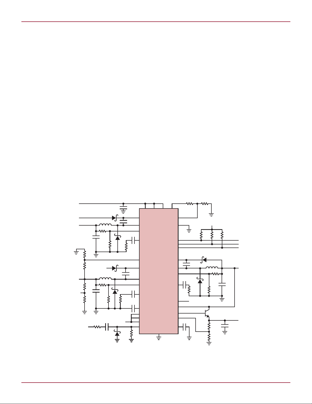
Figure 1. The LT3507 in a wide input range, quad output application
25
EFFICIENCY (%)
LOAD CURRENT (A)
2.50
90
50
0.5 1 1.5 2
70
60
80
CHANNEL 3
5V
OUT
CHANNEL 2
3.3V
OUT
CHANNEL 1
1.8V
OUT
VIN = 12V
V
OUT2
20mV/DIV
LDO
V
OUT4
20mV/DIV
2µs/DIV
L DESIGN FEATURES
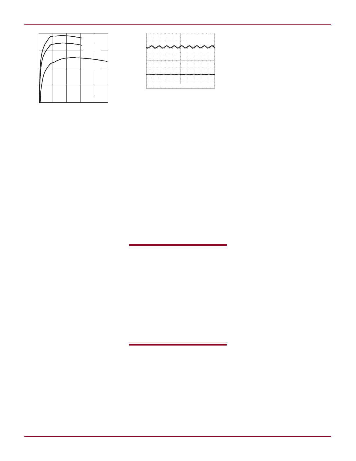
Figure 2. Switching regulator efficiency
architecture, which simplifies loop
compensation. External compensation allows custom tailoring of loop
bandwidth, transient response and
phase margin. The feedback reference
is 0.8V, allowing output voltages as
low as 0.8V.
The regulators share a master oscillator that is resistor programmable
from 250kHz to 2.5MHz, or can be
synchronized to an external frequency
in the same range. Each regulator features frequency foldback in overload
conditions to improve short circuit
tolerance. Channel 1 operates 180° out
of phase with respect to channels 2 and
3 to reduce input current ripple.
…and a Low Dropout
Linear Regulator
The LT3507 also includes an LDO
linear regulator that uses an external
NPN pass transistor to provide up
to 0.5A of output current. The base
drive can supply up to 10mA of base
current to the pass transistor and is
current limited. The LDO is internally
compensated and is stable with output
capacitance of 2.2µF or greater. It uses
the same 0.8V feedback reference as
the switching regulators.
The LDO drive current is drawn
from the BIAS pin if it’s at least 1.5V
higher than the DRIVE pin voltage,
otherwise it’s drawn from V
reduces the power consumption of
the LDO, especially when V
high voltages.
The LDO does not have a separate
RUN pin; it is powered up when any of
the RUN pins are high. The LDO can
be shut down when it is not used by
pulling the FB pin above 1.25V with at
26
. This
IN1
is at
IN1
Figure 3. The LT3507’s built-in
LDO offers a low noise output
least 30µA. If independent control of
the LDO is needed, the LDO output can
be forced to 0V by pulling the TRK/SS4
pin low. If the track or soft-start functions are needed, use an open drain
output in parallel with the track or
soft-start circuitry described below. If
track and soft-start are not necessary,
then a standard CMOS output (from
1.8V to 5V) is sufficient.
Run Control
Each of the switching regulators has
a RUN pin to allow flexibility in shutting off power domains. The RUN pin
The LT3507 includes three
independent, monolithic
switching regulators to
achieve a space saving
solution. Each of the three
switching regulators has its
own input supply pin to the
power switch. The regulators
may be operated from
different supplies in order to
maximize system efficiency.
is a wide range logic input and can be
driven from 1.8V CMOS logic, directly
from VIN (up to 36V), or anywhere in
between. The RUN pin draws a small
amount of current to bring the reference up. This current is about 3µA at
1.8V and 40µA at 36V. The RUN pin
should be pulled low (not left floating)
when the regulator is to be shut down.
When all three RUN pins are pulled
low, the LT3507 goes into a low power
shut down state and draws less than
1µA from the input supply.
Track/Soft-Start Control
Each regulator and the LDO has its
own track/soft-start (TRK/SS) pin.
When this pin is below the 0.8V reference, the regulator forces its feedback
pin to the TRK/SS pin voltage rather
than to the reference voltage. The
TRK/SS pin has a 1.25µA pull-up
current source. The soft-start function
requires a capacitor from the TRK/SS
pin to ground. At start-up, this capacitor is at 0V, which forces the regulator
outputs to 0V. The current source
slowly charges the capacitor voltage
up and the regulator outputs ramp
up proportionally. Once the capacitor
voltage reaches 0.8V, the regulator
locks onto the internal reference instead of the TRK/SS voltage.
The tracking function is achieved
by connecting the slave regulator’s
TRK/SS pin to a resistor divider from
the master regulator output. The
master regulator uses a normal softstart capacitor as described above to
generate the start-up ramp that controls the other regulators. The resistor
divider ratio sets the type of tracking,
either coincident (ratio equal to slave
feedback divider ratio) or ratiometric
(ratio equal to master feedback divider
ratio plus a small offset).
Undervoltage and
Overvoltage Protection
Each switching regulator has its
own input undervoltage shutdown
to prevent the circuit from operating
erratically in undervoltage conditions.
V
shuts down at 4.0V, and because
IN1
it’s the primary input voltage, it turns
off the entire LT3507. V
shut off at 3.0V and only shut off the
switch on the affected channel.
The LT3507 also has a user
programmable undervoltage and
overvoltage lockout. The undervoltage
lockout can protect against pulse
stretching and regulator dropout.
It can also protect the input source
from excessive current since the buck
regulator is a constant power load and
draws more current when the input
source is low. The overvoltage lockout
Linear Technology Magazine • June 2008
and V
IN2
IN3

DESIGN FEATURES L
1V/DIV
V
OUT3
V
OUT2
V
OUT4
V
OUT1
1ms/DIV
Authors can be contacted
at (408) 432-1900
can protect the rectifier diodes from
excessive reverse voltage and can
prevent pulse-skipping by limiting the
minimum duty cycle. Both of these
lockouts shut off all four regulators
when tripped.
These functions are realized with
a pair of built in comparators at
inputs UVLO and OVLO. A resistor
divider from the VINSW pin to each
comparator input sets the trip voltage
and hysteresis. The VINSW pin pulls
up to V
when any RUN pin is pulled
IN1
high, and is open when all three RUN
pins are low. This reduces shutdown
current by disconnecting the resistor
dividers from the input voltage. These
comparators have a 1.2V threshold
and also have 10µA of hysteresis.
The UVLO hysteresis is a current sink
while the OVLO hysteresis is a current
source. UVLO should be connected to
VINSW and OVLO connected to ground
if these functions aren’t used.
Frequency Control
The switching frequency is set by a
single resistor to the RT/SYNC pin.
The value is adjustable from 250kHz
to 2.5MHz. Higher frequencies allow
smaller inductors and capacitors, but
efficiency is lower and the supply has
a smaller allowable range of step-down
ratios due to the minimum on and off
time constraints.
The frequency can also be synchronized to an external clock by
connecting it to the RT/SYNC pin. The
clock source must supply a clock signal
whenever the LT3507 is powered up.
This leads to a dilemma if the clock
source is to be powered from one of the
LT3507 regulators: there is no clock
until the regulator comes up, but the
regulator won’t come up until there’s a
clock! This situation is easily overcome
with a capacitor, a low leakage diode
and a couple of resistors. The capacitor isolates the clock source from the
RT/SYNC pin until the power is up
and the resistor on the RT/SYNC pin
sets the initial clock frequency. The
application in Figure 1 shows how
this is done.
Typical Application
Figure 1 shows a typical LT3507 application. This application allows a
very wide input range, from 6V to 36V.
It generates four outputs: 5V, 3.3V,
2.5V and 1.8V. Efficiencies for three
of the outputs are shown in Figure 2.
The LDO produces a particularly low
noise output at 2.5V, as shown in
Figure 3.
The outputs are set to coincident
tracking using the 5V supply as the
Figure 4. Coincident tracking waveforms
master. But wait, there’s no resistor
divider on the TRK/SS4 pin! It’s no
mistake; the LDO output coincidently
tracks the supply it’s sourced from
(the 3.3V supply in this case) as long
as Q1 is a low V
transistor, such
CESAT
as the NSS30101 used here. Just
remember that this little cheat only
works for coincident tracking. Figure 4
shows the start-up waveforms of the
four outputs.
In this application, the clock is
synchronized to an external source
that is powered from the 3.3V output.
A capacitor isolates the clock until the
3.3V supply is good, and then passes
the clock signal to the RT/SYNC pin.
It should be noted that the LDO can
actually supply up to 0.5A as long as
I
OUT4
+ I
OUT2
≤ 1.5A.
Conclusion
The LT3507 provides a compact
solution for four power supplies. Its
tiny 5mm × 7mm QFN package includes three highly efficient switching
regulators and a low dropout linear
regulator. Just a few small inductors
and ceramic capacitors are needed to
create four high efficiency step-down
regulators. Plenty of options insure
that the LT3507 meets the needs of
a wide variety of multiple output applications.
L
LT5575, continued from page 13
signals as shown in Figure 6. One of
these is a –48dBm CW tone, and the
other is a –48dBm WCDMA carrier.
These are offset in frequency so that
the resulting 3rd order product appears centered about DC. Compute the
intermodulation product generated in
the I/Q demodulator:
q
RF gain preceding LT5575: 20dB
q
Signals entering LT5575: –28dBm
q
LT5575 IIP3, 2-tone: 22.6dBm
q
LT5575 a3: 0.0244
A MATLAB simulation performed
using a pseudo-random channel pre-
Linear Technology Magazine • June 2008
dicts distortion at LT5575 output of
–135.8dBm. This result agrees well
with the equation 8, which predicts a
distortion power of –135.7dBm.
Refer this signal back to the receiver
input:
q
RF gain preceding LT5575: 20dB
q
Equivalent interference level at
Rx input: –155.8dBm
q
Thermal noise at receiver input:
–101.2dBm
The equivalent interference in this
case is 54.6dB below the thermal noise
at the receiver input. The resulting
degradation in sensitivity is <0.1dB,
so the receiver easily meets the specification of –121dBm.
Conclusion
The calculations given here using the
LT5575 I/Q demodulator show that a
WCDMA wide area basestation receiver
can be successfully implemented using
a direct conversion architecture. The
high 2nd order linearity and input 1dB
compression point of the LT5575 are
critical to meeting the performance
requirements of such a design.
L
27
 Loading...