

Page 1
LT3500
Monolithic 2A Step-Down
Regulator Plus Linear
Regulator/Controller
FEATURES
n
Wide Input Range: 3V to 36V Operating,
40V Maximum
n
Short-Circuit Protected Over Full Input Range
n
2A Output Current Capability
n
Adjustable/Synchronizable Fixed Frequency
Operation from 250kHz to 2.2MHz
n
Soft-Start/Tracking Capability
n
Output Adjustable Down to 0.8V
n
Adjustable Linear Regulator/Driver with 13mA
Output Capability
n
Power Good Comparator with Complimentary
Outputs
n
Low Shutdown Current: 12µA
n
Thermally Enhanced 3mm × 3mm DFN or 16-Pin
MSOP Package
APPLICATIONS
n
Automotive Battery Regulation
n
Industrial Control
n
Wall Transformer Regulation
n
Distributed Power Regulation
DESCRIPTION
The LT®3500 is a current mode PWM step-down DC/DC
converter with an internal 2.3A switch. The wide input range
of 3V to 40V makes the LT3500 suitable for regulating
power from a wide variety of sources, including automotive batteries, 24V industrial supplies and unregulated
wall adapters.
Resistor-programmable 250kHz to 2.2MHz frequency
range and synchronization capability enable optimization
between effi ciency and external component size. Cycleby-cycle current limit, frequency foldback and thermal
shutdown provide protection against a shorted output.
The soft-start feature controls the ramp rate of the output
voltage, eliminating input current surge during start-up,
and also provides output tracking.
The LT3500 contains an internal NPN transistor with feedback control which can be confi gured as a linear regulator
or as a linear regulator controller.
The LT3500’s low current shutdown mode (<12µA) enables
easy power management in battery-powered systems.
L, LT, LTC and LTM are registered trademarks of Linear Technology Corporation.
All other trademarks are the property of their respective owners.
TYPICAL APPLICATION
Dual Step-Down Converters
V
6V TO 36V
0.47µF
53.6k
IN
2.2µF
330pF
40.2k
IN
SHDN
SS
R
T/
V
C
LT3500
SYNC
BSTV
SW
LDRV
LFB
0.47µF
6.8µH
B240A
42.2k
FB
PG
PG
24.9k
8.06k
8.06k
1k
22µF
3500 TA01a
V
3.3V
1A
OUT2
V
5V
1A
22µF
OUT1
90
85
80
75
70
65
EFFICIENCY (%)
60
VIN = 12V
55
I
OUT2
FREQUENCY = 800kHz
50
0
= 0A
0.4 0.8 1.2 2.01.40.2 0.6 1.0 1.8
LOAD CURRENT (A)
1.6
3500 TA01b
V
V
OUT2
OUT1
= 5V AT 1A
AC COUPLED
2mV/DIV
= 3.3V AT 1A
AC COUPLED
2mV/DIV
Output Voltage RippleSwitching Converter Effi ciency
500ns/DIV
3500 TA01c
3500fb
1
Page 2
LT3500
ABSOLUTE MAXIMUM RATINGS
(Note 1)
VIN, PG, PG Operating .................................... 40V/–0.3V
SW ............................................................................. V
IN
BST ................................................................ 55V/–0.3V
BST Pin Above SW ....................................................25V
LDRV, SHDN ..............................................................15V
FB, LFB, R
SS, V
/SYNC .......................................................5V
T
......................................................................2.5V
C
PIN CONFIGURATION
TOP VIEW
1
V
IN
2
SHDN
3
SS
PG
V
C
RT/SYNC
12-LEAD (3mm × 3mm) PLASTIC DFN
EXPOSED PAD (PIN 13) IS GND, MUST BE SOLDERED TO PCB
θJA = 45°C/W, θ
13
4
5
6
DD PACKAGE
JC(PAD)
12
11
10
9
8
7
= 10°C/W
SW
BST
LDRV
LFB
FB
PG
Operating Junction Temperature Range
LT3500EDD (Note 2) .......................... –40°C to 125°C
LT3500IDD (Note 2) ...........................–40°C to 125°C
LT3500HDD (Note 2).......................... –40°C to 150°C
LT3500EMSE (Note 2)........................ –40°C to 125°C
LT3500IMSE (Note 3) ........................ –40°C to 125°C
LT3500HMSE (Note 2) ....................... –40°C to 150°C
Storage Temperature Range ...................–65°C to 150°C
TOP VIEW
1
NC1
2
V
IN
3
SHDN
4
SS
5
PG
6
V
C
7
RT/SYNC
8
NC8
EXPOSED PAD (PIN 17) IS GND, MUST BE SOLDERED TO PCB
θJA = 45°C/W, θ
17
MSE PACKAGE
16-LEAD PLASTIC MSE
JC(PAD)
16
15
14
13
12
11
10
9
= 10°C/W
NC16
SW
BST
LDRV
LFB
FB
PG
NC9
ORDER INFORMATION
LEAD FREE FINISH TAPE AND REEL PART MARKING* PACKAGE DESCRIPTION TEMPERATURE RANGE
LT3500EDD#PBF LT3500EDD#TRPBF LCRN
LT3500IDD#PBF LT3500IDD#TRPBF LCRN
LT3500HDD#PBF LT3500HDD#TRPBF LDCY
12-Lead (3mm × 3mm) Plastic DFN
12-Lead (3mm × 3mm) Plastic DFN
12-Lead (3mm × 3mm) Plastic DFN
LT3500EMSE#PBF LT3500EMSE#TRPBF 3500 16-Lead Plastic MSE –40°C to 125°C
LT3500IMSE#PBF LT3500IMSE#TRPBF 3500 16-Lead Plastic MSE –40°C to 125°C
LT3500HMSE#PBF LT3500HMSE#TRPBF 3500 16-Lead Plastic MSE –40°C to 150°C
Consult LTC Marketing for parts specifi ed with wider operating temperature ranges. *The temperature grade is identifi ed by a label on the shipping container.
Consult LTC Marketing for information on non-standard lead based fi nish parts.
For more information on lead free part marking, go to: http://www.linear.com/leadfree/
For more information on tape and reel specifi
cations, go to: http://www.linear.com/tapeandreel/
–40°C to 125°C
–40°C to 125°C
–40°C to 150°C
3500fb
2
Page 3
LT3500
The l denotes the specifi cations which apply over the full operating
ELECTRICAL CHARACTERISTICS
temperature range, otherwise specifi cations are at T
= 25°C. V
J
PARAMETER CONDITIONS MIN TYP MAX UNITS
SHDN Threshold
SHDN Source Current V
= 0.62V 1.5 2.5 3.5 µA
SHDN
SHDN Current Hysterisis 1.25 2 3.25 µA
Minimum Input Voltage (Note 3) V
Supply Shutdown Current V
Supply Quiescent Current V
FB Voltage V
FB Bias Current V
Error Amplifi er g
m
Error Amplifi er Source Current V
Error Amplifi er Sink Current V
Error Amplifi er High Clamp V
Error Amplifi er Switching Threshold V
SS Source Current V
SS Sink Current V
SS POR Sink Current (Note 4) V
= 0V
FB
= 0V
SHDN
= 0.9V 2.5 3.5 mA
FB
= 1V
VC
V
= 0.8V to 1.6V, VIN = 3V to 40V
VC
= 0.8V, VVC = 1V 50 150 nA
FB
VVC = 1V, IVC = ±10µA 150 250 350 µmho
= 0.6V, VVC = 1V 12 16 20 µA
FB
= 1V, VVC = 1V 14 18 22 µA
FB
= 0.6V 1.8 2.0 2.2 V
FB
= 0.6V 0.6 0.8 1.0 V
FB
= 0.4V, VFB = 0.9V 2.25 2.75 3.75 µA
SS
= 0V, VSS = 2V 300 600 900 µA
FB
= 0V, VSS = 2V, Cycle SHDN 400 600 800 µA
FB
SS POR Threshold 50 100 150 mV
SS to FB Offset (V
– VFB)V
SS
PG/PG Leakage V
PG/PG Threshold (Rising) V
PG/PG Hysteresis (Falling) V
PG Sink Current V
PG Sink Current V
/SYNC Reference Voltage VFB = 0.9V, R
R
T
Switching Frequency R
= VFS, VSS = 0.4V 70 100 120 mV
VC
= 0.9V, VPG/VPG = 40V 0.1 1 µA
FB
= 0.4V 0.685 0.708 0.730 V
PG
= 0.4V 20 30 40 mV
PG
= 0.4V, VFB = 0.7V 250 500 750 µA
PG
= 0.4V, VFB = 0.9V 500 800 1100 µA
PG
RT/SYNC
= 90.9k
RT/SYNC
R
R
RT/SYNC
RT/SYNC
= 90.9k
= 15k
SYNC Frequency Range
Minimum Switch On Time V
Minimum Switch Off Time V
= 0.7V, R
FB
= 0.7V, R
FB
RT/SYNC
RT/SYNC
Switch Leakage Current VSW = 0V 1 10 µA
Switch Saturation Voltage I
Switch Peak Current DD Package V
Switch Peak Current MSE Package V
Boost Current I
Minimum Boost Voltage (Note 5) I
= 2A, V
SW
= 18V, VFB = 0.7V
BST
= 18V, VFB = 0.7V
BST
= 2A, V
SW
= 2A, VFB = 0.7V 2.2 3 V
SW
= 18V, VFB = 0.7V 450 mV
BST
= 20V, VFB = 0.7V 20 30 45 mA
BST
= 15V, V
VIN
= 2V, unless otherwise specifi ed.
RT/SYNC
l
l
l
l
l
710 760 780 mV
2.4 2.8 V
12 30 µA
0.784
0.776
0.8
0.8
0.816
0.824
= 15k 0.75 0.850 0.975 V
450
l
425
2
l
250 2500 kHz
500
500
2.4
550
625
2.8
kHz
kHz
MHz
= 90.9k 140 ns
= 90.9k 120 ns
2.3
l
2.1
2.3
l
2.1
2.8
2.8
2.9
2.9
3.5
3.5
3.5
3.7
V
V
A
A
A
A
3500fb
3
Page 4
LT3500
ELECTRICAL CHARACTERISTICS
The l denotes the specifi cations which apply over the full operating
temperature range, otherwise specifi cations are at T
= 25°C. V
J
PARAMETER CONDITIONS MIN TYP MAX UNITS
LFB Voltage V
LFB Line/Load Regulation V
– V
SS to LFB Offset (V
SS
)V
LFB
LFB Bias Current V
– V
LDRV Dropout (V
VIN
)V
LDRV
LDRV Maximum Current V
= V
LDRV
LFB
= 3V to 40V, V
VIN
= 0.8V, V
SS
LFB
LDRV
LDRV
LDRV
= 0.8V 115 300 nA
= 3V, I
LDRV
= 5mA
= 0V
LDRV
= V
VIN
= V
LFB
= 15V, V
LFB
= 2V, unless otherwise specifi ed.
RT/SYNC
l
l
l
l
0.784 0.8 0.816 V
0.776 0.8 0.824 V
90 115 140 mV
0.8 1.2 1.6 V
91318mA
Note 1: Stresses beyond those listed under Absolute Maximum Ratings
may cause permanent damage to the device. Exposure to any Absolute
Maximum Rating condition for extended periods may affect device
reliability and lifetime.
Note2: The LT3500EDD/LT3500EMSE is guaranteed to meet performance
specifi cations from 0°C to 125°C junction temperature. Specifi cations over
the –40°C to 125°C operating junction temperature range are assured by
design, characterization and correlation with statistical process controls.
The LT3500IDD/LT3500IMSE is guaranteed over the full –40°C to 125°C
operating junction temperature range. The LT3500HDD/LT3500HMSE is
guaranteed over the full –40°C to 150°C operating junction temperature
range. High junction temperatures degrade operating lifetimes. Operating
lifetime is derated at junction temperatures greater than 125°C.
Note 3: Minimum input voltage is defi ned as the voltage where internal
bias lines are regulated so that the reference voltage and oscillator remain
constant. Actual minimum input voltage to maintain a regulated output
will depend upon output voltage and load current. See Applications
Information.
Note 4: An internal power-on reset (POR) latch is set on the positive
transition of the SHDN pin through its threshold. The output of the latch
activates a current source on the SS pin which typically sinks 600µA,
discharging the SS capacitor. The latch is reset when the SS pin is driven
below the soft-start POR threshold or the SHDN pin is taken below its
threshold.
Note 5: This is the minimum voltage across the boost capacitor needed to
guarantee full saturation of the internal power switch.
Note 6: This IC includes overtemperature protection that is intended
to protect the device during momentary overload conditions. Junction
temperature will exceed the maximum operating junction temperature
when overtemperature protection is active. Continuous operation above
the specifi ed maximum operating junction temperature may impair device
reliability.
TYPICAL PERFORMANCE CHARACTERISTICS
Feedback Voltage vs Temperature
0.820
0.815
0.810
0.805
0.800
VOLTAGE (V)
0.795
0.790
0.785
0.780
–50
–25
0
TEMPERATURE (°C)
FB
50
25
75
LFB
100
125
150
3500 G01
RT/SYNC Voltage vs Temperature
1.10
1.08
1.06
R
= 90.9k
1.04
1.02
1.00
0.98
VOLTAGE (V)
0.96
0.94
0.92
0.90
RT/SYNC
R
–50
–25 25
= 15k
RT/SYNC
0
TEMPERATURE (°C)
50
75
100
125
3500 G02
150
Shutdown Threshold and Minimum
Input Voltage vs Temperature
3.0
2.5
2.0
1.5
VOLTAGE (V)
1.0
0.5
0
–50
MINIMUM INPUT VOLTAGE
SHUTDOWN THRESHOLD
50 100 150125
–25 0
25 75
TEMPERATURE (°C)
3500 G03
4
3500fb
Page 5
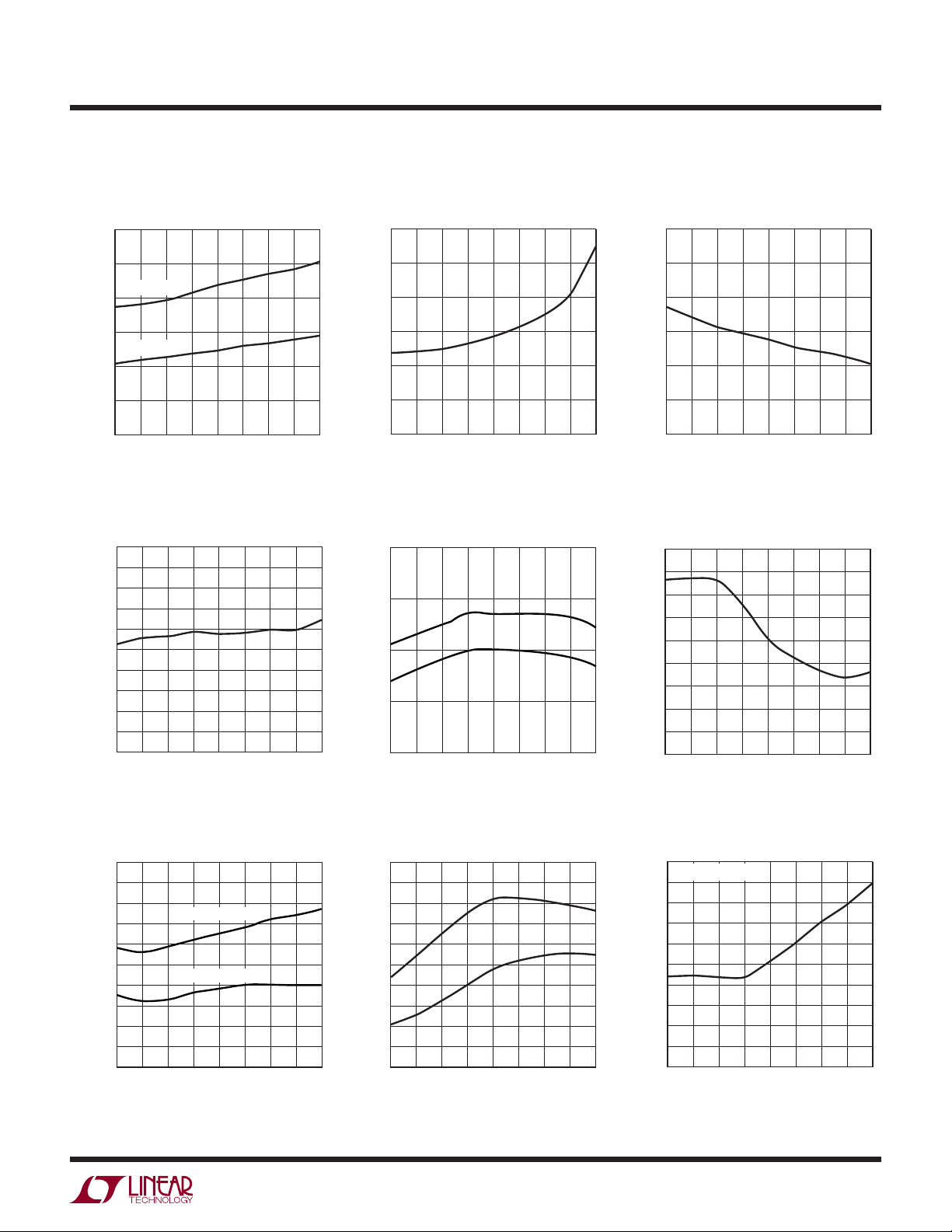
TYPICAL PERFORMANCE CHARACTERISTICS
LT3500
Shutdown Input Currents
vs Temperature
6
5
V
= 0.9V
SHDN
4
3
V
= 0.7V
SHDN
CURRENT (µA)
2
1
0
–50
050
–25 25
TEMPERATURE (°C)
Soft-Start Source Current
vs Temperature
3.5
3.3
3.1
2.9
2.7
2.5
2.3
CURRENT (µA)
2.1
1.9
1.7
1.5
–50
–25 25
0
TEMPERATURE (°C)
Shutdown Quiescent Current
vs Temperature
15.0
12.5
10.0
7.5
CURRENT (µA)
5.0
2.5
0
100
75
125
150
3500 G04
–50
050
–25 25
TEMPERATURE (°C)
100
75
125
150
3500 G05
Soft-Start Feedback Offset
vs Temperature
150
125
LFB
100
VOLTAGE (mV)
75
125
50
100
75
150
3500 G07
50
FB
–50
–25 0 25 50
TEMPERATURE (°C)
75 100 125 150
3500 G08
Error Amplifi er gm vs Temperature
400
350
300
250
200
TRANSCONDUCTANCE (µmhos)
150
100
–50
–25 25
050
TEMPERATURE (°C)
75
VC Switching Threshold
vs Temperature
0.95
0.90
0.85
0.80
0.75
0.70
VOLTAGE (V)
0.65
0.60
0.55
0.50
–50
–25
0
25 150125
50
TEMPERATURE (°C)
75 100
100
125
3500 G09
150
3500 G06
Power Good Thresholds
vs Temperature
0.75
0.74
0.73
0.72
0.71
0.70
0.69
VOLTAGE (V)
0.68
0.67
0.66
0.65
–50
–25
RISING EDGE
FALLING EDGE
25
0
TEMPERATURE (°C)
Power Good Sink Currents
vs Temperature Frequency vs Temperature
1000
900
800
700
600
500
400
CURRENT (µA)
300
200
100
50
75
100
150125
3500 G10
0
–50
–25
PG
PG
50
25
0
TEMPERATURE (°C)
75
100
150125
3500 G11
600
R
RT/SYNC
580
560
540
520
500
480
FREQUENCY (kHz)
460
440
420
400
–50
–25
= 90.9k
50
25
0
TEMPERATURE (°C)
75
100
150125
3500 G12
3500fb
5
Page 6
LT3500
TYPICAL PERFORMANCE CHARACTERISTICS
Peak Switch Current
vs Temperature
3.5
3.4
3.3
3.2
3.1
3.0
2.9
CURRENT (A)
2.8
2.7
2.6
2.5
–50
DD PACKAGE
–25
0
TEMPERATURE (°C)
MSE PACKAGE
50
25
75
100
150125
3500 G13
LDRV Short-Circuit Current
vs Temperature
20
19
18
17
16
15
14
CURRENT (mA)
13
12
11
10
–50
Minimum Switching Times Frequency vs R
300
275
250
225
200
175
TIME (ns)
150
125
100
75
50
–50
MINIMUM ON TIME
–25 25
0
TEMPERATURE (°C)
MINIMUM OFF TIME
50
100
75
125
150
3500 G16
2500
2250
2000
1750
1500
1250
1000
FREQUENCY (kHz)
750
500
250
0
0
–25
0
4020
50
25
TEMPERATURE (°C)
75
RT/SYNC
120 140 180
8060
100
R
(kΩ)
RT/SYNC
100
TA = 25°C
160
3500 G14
3500 G17
150125
200
External Sync Duty Cycle Range
vs External Sync Frequency
100
90
80
70
60
50
40
DUTY CYCLE (%)
30
20
10
0
250
MAXIMUM DUTY CYCLE
= 25°C
T
A
MINIMUM DUTY CYCLE
750
SYNCHRONIZATION FREQUENCY (kHz)
1250
1750
Switch Saturation Voltage
vs Switch Current
600
500
400
300
–50°C
200
100
SWITCH SATURATION VOLTAGE (mV)
0
25°C
150°C
0.4 0.8 1.2 1.6
SWITCH CURRENT (A)
2250
3500 G15
2.00.20 0.6 1.0 1.4 1.8
3500 G18
Boost Current vs Switch Current
50
45
40
35
30
25
20
15
BOOST CURRENT (mA)
10
5
0
0.40.2
0
–50°C
0.80.6
1.0
SWITCH CURRENT (A)
6
150°C
25°C
1.2 1.4 1.8
1.6
3500 G19
2.0
Minimum Boost Voltages
vs Temperature Minimum Input Voltage
2.7
2.5
2.3
2.1
MINIMUM BOOST FOR
SWITCH SATURATION
1.9
BOOST VOLTAGE (V)
1.7
1.5
–50
050
–25 25
TEMPERATURE (°C)
75
100
125
150
3500 G20
8
TA = 25°C
7
6
5
4
3
INPUT VOLTAGE (V)
2
1
fSW = 1MHz
L = 3.3µH
0
0.4 0.8 1.2 2.01.40.2 0.6 1.0 1.8
0
V
OUT1
V
OUT1
LOAD CURRENT (A)
= 5V
= 3.3V
1.6
3500 G21
3500fb
Page 7
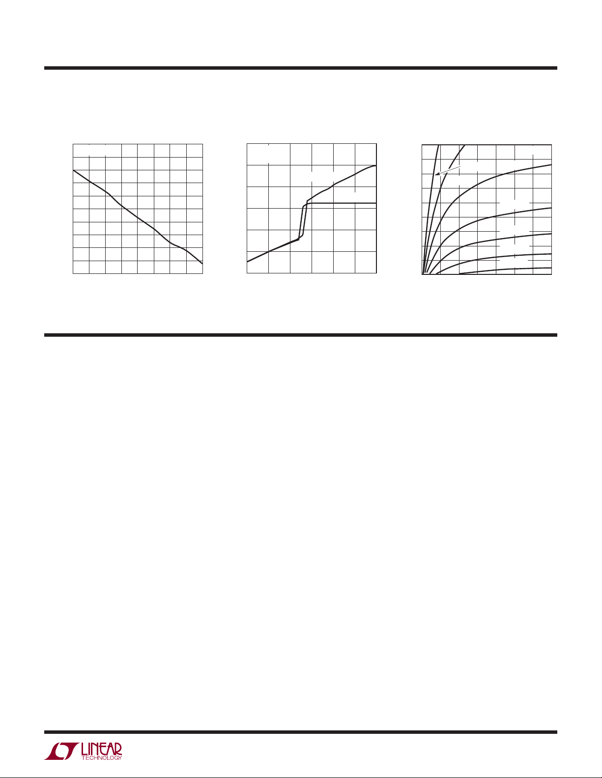
TYPICAL PERFORMANCE CHARACTERISTICS
LDRV Dropout Voltage
vs Temperature
1.50
I
LDRV
1.45
1.40
1.35
1.30
1.25
1.20
VOLTAGE (V)
1.15
1.10
1.05
1.00
–50
= 5mA
–25 25
0
TEMPERATURE (°C)
125
50
100
75
150
3500 G22
Switcher Dropout Operation
6
I
= 1A
VOUT1
= 25°C
T
A
5
V
4
3
2
OUTPUT VOLTAGE (V)
1
0
2.5
3.5 4.0 4.5
3.0
INPUT VOLTAGE (V)
VOUT1
= 5V
V
VOUT1
= 3.3V
5.0 5.5
3500 G23
Inductor Value for 2A Maximum
Load Current (V
I
RIPPLE
2500
2250
2000
1750
1500
1250
1000
FREQUENCY (kHz)
750
500
250
5
10
= 250mA)
L = 1.5µH
OUT1
L = 1µH
15
20 40
INPUT VOLTAGE (V)
25
LT3500
= 3.3V,
TA = 25°C
L = 2.2µH
L = 3.3µH
L = 4.7µH
L = 6.8µH
L = 10µH
30 35
3500 G24
PIN FUNCTIONS
VIN: The VIN pin powers the internal control circuitry and
is monitored by an undervoltage comparator. The V
is also connected to the collectors of the internal power
NPN switch and linear output NPN. The V
pin has high
IN
dI/dt edges and must be decoupled to ground close to
the pin of the device.
SHDN: The SHDN pin is used to shut down the LT3500
and reduce quiescent current to a typical value of
12µA. The accurate 0.76V threshold and input current
hysteresis can be used as an undervoltage lockout, preventing the regulator from operating until the input voltage has
reached a predetermined level. Force the SHDN pin above
its threshold or let it fl oat for normal operation.
SS: The SS pin is used to control the slew rate of the
output of both the switching and linear regulators. A
single capacitor from the SS pin to ground determines
the regulators’ ramp rate. For soft-start details see the
Applications Information section.
PG: The power good pin is an open-collector output that
sinks current when the FB or LFB falls below 90% of its
IN
pin
nominal regulating voltage. For V
state remains true, although during SHDN, V
above 2V, its output
IN
undervoltage
IN
lockout, or thermal shutdown, its current sink capability
is reduced
: The VC pin is the output of the error amplifi er and the
V
C
input to the peak switch current comparator. It is normally
used for frequency compensation, but can also be used
as a current clamp or control loop override. If the error
amplifi er drives V
above the maximum switch current
C
level, a voltage clamp activates. This indicates that the
output is overloaded and current to be pulled from the
SS pin reducing the regulation point.
/SYNC: This RT/SYNC pin provides two modes of setting
R
T
the constant switch frequency.
Connecting a resistor from the R
will set the R
/SYNC pin to a typical value of 1V. The
T
/SYNC pin to ground
T
resultant switching frequency will be set by the resistor
value. The minimum value of 15kΩ and maximum value
of 200kΩ set the switching frequency to 2.5MHz and
250kHz respectively.
3500fb
7
Page 8

LT3500
PIN FUNCTIONS
Driving the RT/SYNC pin with an external clock signal
will synchronize the switch to the applied frequency.
Synchronization occurs on the rising edge of the clock
signal after the clock signal is detected. Each rising clock
edge initiates an oscillator ramp reset. A gain control loop
servos the oscillator charging current to maintain a constant oscillator amplitude. Hence, the slope compensation
remains unchanged. If the clock signal is removed, the
oscillator reverts to resistor mode and reapplies the 1V
bias to the R
circuitry times out. The clock source impedance should
be set such that the current out of the R
resistor mode generates a frequency roughly equivalent
to the synchronization frequency. Floating or holding the
/SYNC pin above 1.1V will not damage the device, but
R
T
will halt oscillation.
PG: The power good bar pin is an open-collector output
that sinks current when the FB or LFB rises above 90%
of its nominal regulating voltage.
FB: The FB pin is the negative input to the switcher error
amplifi er. The output switches to regulate this pin to 0.8V
with respect to the exposed ground pad. Bias current
fl ows out of the FB pin.
LFB: The LFB pin is the negative input to the linear error
amplifi er. The L
with respect to the exposed ground pad. Bias current fl ows
out of the LFB pin.
/SYNC pin after the synchronization detection
T
/SYNC pin in
T
pin servo’s to regulate this pin to 0.8V
DRV
LDRV: The LDRV pin is the emitter of an internal NPN that
can be confi gured as an output of a linear regulator or as
the drive for an external NPN high current regulator. Current fl ows out of the LDRV pin when the LFB pin voltage is
below 0.8V. The LDRV pin has a typical maximum current
capability of 13mA.
BST: The BST pin provides a higher than V
the power NPN to ensure a low switch drop. A comparator to V
the BST pin voltage drops too low. Forcing a SW off time
allows the boost capacitor to recharge.
SW: The SW pin is the emitter of the on-chip power NPN.
At switch off, the inductor will drive this pin below ground
with a high dV/dt. An external catch diode to ground, close
to the SW pin and respective V
ground, must be used to prevent this pin from excessive
negative voltages.
Exposed Pad: GND. The Exposed Pad is the only ground
connection for the device. The Exposed Pad should be
soldered to a large copper area to reduce thermal resistance. The GND pin also serves as small-signal ground.
For ideal operation all small-signal ground paths should
connect to the GND pin at a single point, avoiding any
high current ground returns.
NC Pins (MSE Package Only): No Connection. The NC pins
are electrically isolated from the LT3500. The NC pins may
be connected to PCB traces to aid PCB layout.
imposes a minimum off time on the SW pin if
IN
decoupling capacitor’s
IN
base drive to
IN
8
3500fb
Page 9
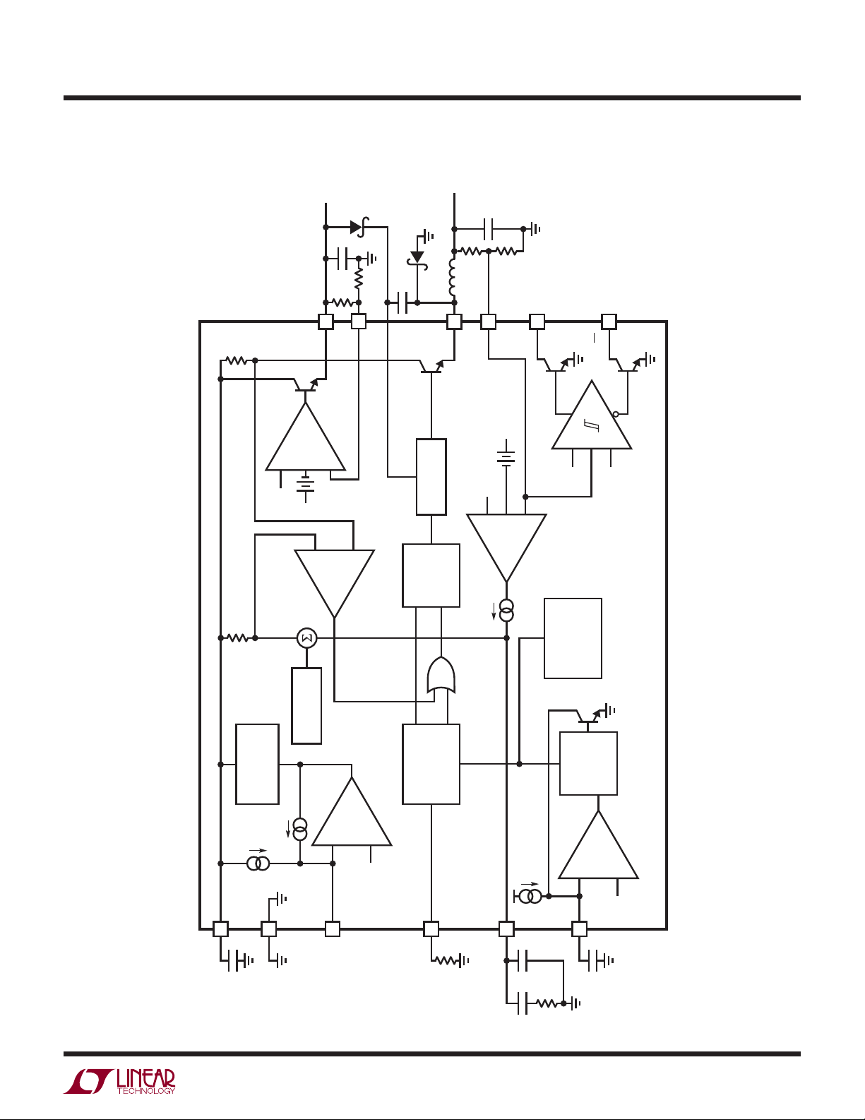
BLOCK DIAGRAM
–
+
–
+
+
–
+
+
–
+
–
–
+
INTERNAL
REGULATOR
AND REFERENCES
OSCILLATOR
AND AGC
POWER ON RESET
THERMAL
OVERLOAD
SQR
PRE
SQR
2µA
2.75µA
2.5µA
C1
0.76V
–
+
100mV
R5
R6
V
IN
GND
SHDN
R
T
/SYNC
V
C
SS
DRIVER
CIRCUITRY
SLOPE
COMPENSATION
0.8V
SS
115mV
LDRV
R3
R1
R2
R4
C5
D2
D1
V
OUT2
V
OUT1
3500 BD
LFB
SW
FB
PG
PG
0.8V
100mV
0.7V
LFB
SS
C6
L1
C2
C4C3
C7
+
+
LT3500
Figure 1. LT3500 Block Diagram
3500fb
9
Page 10

LT3500
OPERATION
The LT3500 is a constant frequency, current mode buck
converter with an internal 2.3A switch plus a linear regulator with 13mA output capability. Control of both outputs
is achieved with a common SHDN pin, internal regulator,
oscillator, undervoltage detect, soft-start, thermal shutdown and power-on reset.
If the SHDN pin is taken below its 0.8V threshold, the
LT3500 will be placed in a low quiescent current mode.
In this mode the LT3500 typically draws 12µA from the
pin.
V
IN
When the SHDN pin is fl oated or driven above 0.76V, the
internal bias circuits turn on generating an internal regulated voltage, 0.8(V
) and 1V(RT/SYNC) references, and
FB
a POR signal which sets the soft-start latch.
As the R
/SYNC pin reaches its 1V regulation point, the
T
internal oscillator will start generating a clock signal at a
frequency determined by the resistor from the R
/SYNC
T
pin to ground. Alternatively, if a synchronization signal is
detected by the LT3500 at the R
/SYNC pin, a clock signal
T
will be generated at the incoming frequency on the rising
edge of the synchronization pulse. In addition, the internal
slope compensation will be automatically adjusted to prevent subharmonic oscillation during synchronization.
The LT3500 is a constant frequency, current mode stepdown converter. Current mode regulators are controlled
by an internal clock and two feedback loops that control
the duty cycle of the power switch. In addition to the
normal error amplifi er, there is a current sense amplifi er
that monitors switch current on a cycle-by-cycle basis.
This technique means that the error amplifi er commands
current to be delivered to the output rather than voltage.
A voltage fed system will have low phase shift up to the
resonant frequency of the inductor and output capacitor,
then an abrupt 180° shift will occur. The current fed system
will have 90° phase shift at a much lower frequency, but
will not have the additional 90° shift until well beyond
the LC resonant frequency. This makes it much easier to
frequency compensate the feedback loop and also gives
much quicker transient response.
During power up, the POR signal sets the soft-start latch,
which discharges the SS pin to ensure proper start-up
operation. When the SS pin voltage drops below 100mV,
pin is driven low disabling switching and the soft-
the V
C
start latch is reset. Once the latch is reset the soft-start
capacitor starts to charge with a typical value of 2.75µA.
As the voltage rises above 100mV on the SS pin, the V
C
pin will be driven high by the error amplifi er. When the
voltage on the V
pin exceeds 0.8V, the clock set-pulse sets
C
the driver fl ip-fl op which turns on the internal power NPN
switch. This causes current from V
, through the NPN
IN
switch, inductor and internal sense resistor, to increase.
When the voltage drop across the internal sense resistor
exceeds a predetermined level set by the voltage on the
pin, the fl ip-fl op is reset and the internal NPN switch
V
C
is turned off. Once the switch is turned off the inductor
will drive the voltage at the SW pin low until the external
Schottky diode starts to conduct, decreasing the current
in the inductor. The cycle is repeated with the start of each
clock cycle. However, if the internal sense resistor voltage
exceeds the predetermined level at the start of a clock cycle,
the fl ip-fl op will not be set resulting in a further decrease in
inductor current. Since the output current is controlled by
voltage, output regulation is achieved by the error
the V
C
amplifi er continually adjusting the V
pin voltage.
C
The error amplifi er is a transconductance amplifi er that
compares the FB voltage to either the SS pin voltage minus
100mV or an internally regulated 800mV, whichever is
lowest. Compensation of the loop is easily achieved with
a simple capacitor or series resistor/capacitor from the
pin to ground.
V
C
Since the SS pin is driven by a constant current source, a
single capacitor on the soft-start pin will generate controlled
linear ramp on the output voltage.
If the current demanded by the output exceeds the maximum current dictated by the V
pin clamp, the SS pin
C
will be discharged, lowering the regulation point until the
output voltage can be supported by the maximum current.
When overload is removed, the output will soft-start from
the overload regulation point.
10
3500fb
Page 11

OPERATION
LT3500
VIN undervoltage detection or thermal shutdown will
set the soft-start latch, resulting in a complete soft-start
sequence.
The switch driver operates from either the V
or BST volt-
IN
age. An external diode and capacitor are used to generate
a drive voltage higher than V
to saturate the output NPN
IN
and maintain high effi ciency.
In addition to the switching regulator, the LT3500 contains
a NPN linear regulator with a 0.8V reference, and 13mA
current capability. The 0.8 reference will track the SS pin
APPLICATIONS INFORMATION
Choosing the Output Voltage
The output voltage is programmed with a resistor divider
between the output and the FB pin. Choose the 1% resistors according to:
V
R1= R2
OUT1
0.8V
R2 should be 10.0k or less to avoid bias current errors.
Reference designators refer to the Block Diagram in
Figure 1.
Choosing the Switching Frequency
The LT3500 switching frequency is set by resistor R5 in
Figure 1. The R
Setting resistor R5 sets the current in the R
which determines the oscillator frequency as illustrated
in Figure 2.
The switching frequency is typically set as high as possible to reduce overall solution size. The LT3500 employs
techniques to enhance dropout at high frequencies but
effi ciency and maximum input voltage decrease due to
switching losses and minimum switch on times. The
–1
/SYNC pin is internally regulated at 1V.
T
/SYNC pin
T
in the same manner as the switching regulator. The linear
output can also be confi gured to drive an external NPN to
provide a linear regulator with higher current capability.
A power good comparator with 30mV of hysteresis trips
when both FB and LFB are above 90% of the 0.8V reference. The PG output is an open collector NPN that is off
when the output is in regulation allowing a resistor to pull
the PG pin to a desired voltage. The PG output is an opencollector NPN that is on when the output is in regulation
providing either drive for an output disconnect transistor
or inverted power good logic.
maximum recommended frequency can be approximated
by the equation:
Frequency (Hz)=
where
VD is the forward voltage drop of the catch diode
(D1 Figure 1),
switch, and t
+ V
OUT1
VIN− VSW+ V
D
D
VSW is the voltage drop of the internal
ON(MIN)
is the minimum on time of the
•
t
ON(MIN)
1
V
switch, all at maximum load current.
2500
2250
2000
1750
1500
1250
1000
FREQUENCY (kHz)
750
500
250
0
Figure 2. Frequency vs RT/SYNC Resistance
4020
0
8060
R
RT/SYNC
120 140 180
100
(kΩ)
160
200
3500 F02
3500fb
11
Page 12

LT3500
APPLICATIONS INFORMATION
The following example along with the data in Table 1
illustrates the tradeoffs of switch frequency selection.
Example.
= 25V, V
V
IN
OUT1
= 3.3V, I
OUT1
= 2.0A,
Temperature = 0°C to 85°C
t
ON(MIN)
tics graph),
Max Frequency =
= 185ns (85°C from Typical Characteris-
VD
= 0.6V,
3.3 + 0.6
25 − 0.4+ 0.6
VSW = 0.4V (85°C)
1
•
~ 835kHz
185ns
RT/SYNC ~ 49.9k
Frequency ≅ 820kHz
Input Voltage Range
Once the switching frequency has been determined, the
input voltage range of the regulator can be determined.
The minimum input voltage is determined by either the
LT3500’s minimum operating voltage of ~2.8V or by its
maximum duty cycle. The duty cycle is the fraction of time
that the internal switch is on during a clock cycle. The
maximum duty cycle can be determined from the clock
frequency and the minimum off time from the typical
characteristics graph.
This leads to a minimum input voltage of:
V
+ V
V
IN(MIN)
OUT1
=
DC
MAX
D
− VD+ V
SW
where VSW is the voltage drop of the internal switch,
and
DC
MAX
= 1 – t
OFF(MIN)
• Frequency.
Figure 3 shows a typical graph of minimum input voltage
vs load current for 3.3V and 5V applications.
The maximum input voltage is determined by the absolute
maximum ratings of the V
and BST pins and by the
IN
frequency and minimum duty cycle.
The minimum duty cycle is defi ned as:
DC
MIN
= t
ON(MIN)
• Frequency
Maximum input voltage as:
V
+ V
V
IN(MAX)
Figure 3. Minimum Input Voltage vs Load Current
OUT1
=
DC
8
7
6
5
4
INPUT VOLTAGE (V)
3
2
0
0.2 0.4 0.6 0.8 1.41.2
D
− VD+ V
MIN
V
V
V
V
1.0 1.6 1.8
LOAD CURRENT (A)
SW
= 5V START-UP
OUT1
= 5V RUNNING
OUT1
= 3.3V START-UP
OUT1
= 3.3V RUNNING
OUT1
fSW = 1MHz
L = 3.3µH
2.0
3500 F03
Table 1. Effi ciency and Size Comparisons for Different R
FREQUENCY RT/SYNC EFFICIENCY V
2.5MHz 15k 73.6 12 1µ 10µ 24
2.0MHz 20k 81.5 14 1.5µ 10µ 24
1.5MHz 24.9k 84.5 18 2.2µ 10µ 24
1.0MHz 40.2k 87.3 28 3.3µ 22µ 34
500kHz 90.9k 88.9 36 4.7µ 47µ 40
RT/SYNC
Values, V
IN(MAX)
OUT1
= 3.3V
L C C + L AREA
12
(mm
2
)
3500fb
Page 13
APPLICATIONS INFORMATION
LT3500
Note that the LT3500 will regulate if the input voltage is
taken above the calculated maximum voltage as long as
maximum ratings of the V
and BST pins are not violated.
IN
However operation in this region of input voltage will exhibit
pulse skipping behavior.
Example:
V
OUT1
= 3.3V, I
= 1A, Frequency = 1MHz,
OUT1
Temperature = 25°C,
V
t
= 0.3V, VD = 0.4V, t
SW
OFF(MIN)
DC
V
IN(MIN)
DC
V
IN(MAX)
= 110ns
=1−(110ns)1MHz =89%
MAX
3.3 + 0.4
=
0.89
= t
MIN
ON(MIN)
3.3 + 0.4
=
ON(MIN)
− 0.4+ 0.3= 4.06V
•Frequency = 15%
− 0.4+ 0.3 = 24.57V
0.15
= 150ns,
Inductor Selection and Maximum Output Current
A good fi rst choice for the inductor value is:
(VIN− V
L =
OUT1
VIN•f
)•V
OUT1
For applications with a duty cycle of about 50%, the inductor value should be chosen to obtain an inductor ripple
current less than 40% of peak switch current.
Of course, such a simple design guide will not always result
in the optimum inductor for your application. A larger value
provides a slightly higher maximum load current, and will
reduce the output voltage ripple. If your load is lower than
1.5A, then you can decrease the value of the inductor and
operate with higher ripple current. This allows you to use
a physically smaller inductor, or one with a lower DCR
resulting in higher effi ciency.
The current in the inductor is a triangle wave with an
average value equal to the load current. The peak switch
current is equal to the output current plus half the peak-to
peak inductor ripple current. The LT3500 limits its switch
current in order to protect itself and the system from
overload faults. Therefore, the maximum output current
that the LT3500 will deliver depends on the current limit,
the inductor value, switch frequency, and the input and
output voltages. The inductor is chosen based on output
current requirements, output voltage ripple requirements,
size restrictions and effi ciency goals.
When the switch is off, the inductor sees the output voltage plus the catch diode drop. This gives the peak-to-peak
ripple current in the inductor:
where f is frequency in MHz and L is in µH.
With this value the maximum load current will be ~2A,
independent of input voltage. The inductor’s RMS current
rating must be greater than your maximum load current
and its saturation current should be about 30% higher. To
keep effi ciency high, the series resistance (DCR) should
be less than 0.05.
V
OUT1
+ V
D
1−DC
()
ΔIL=
()
L•f
where f is the switching frequency of the LT3500 and L
is the value of the inductor. The peak inductor and switch
current is:
ΔI
I
SW(PK)=ILPK=IOUT1
L
+
2
3500fb
13
Page 14

LT3500
APPLICATIONS INFORMATION
To maintain output regulation, this peak current must be
. I
less than the LT3500’s switch current limit, I
LIM
LIM
is
guaranteed to be greater than 2.3A over the entire duty
cycle range. The maximum output current is a function
of the chosen inductor value:
I
OUT1(MAX)=ILIM
ΔI
L
−
=2.3 –
2
ΔI
L
2
If the inductor value is chosen so that the ripple current
is small, then the available output current will be near the
switch current limit.
One approach to choosing the inductor is to start with the
simple rule given above, look at the available inductors
and choose one to meet cost or space goals. Then use
these equations to check that the LT3500 will be able to
deliver the required output current. Note again that these
equations assume that the inductor current is continuous.
Discontinuous operation occurs when I
/2 as calculated above.
I
L
is less than
OUT1
Figure 4 illustrates the inductance value needed for a 3.3V
output with a maximum load capability of 2A. Referring
to Figure 4, an inductor value between 3.3µH and 4.7µH
will be suffi cient for a 15V input voltage and a switch
frequency of 750kHz. There are several graphs in the
Typical Performance Characteristics section of this data
sheet that show inductor selection as a function of input
voltage and switch frequency for several popular output
voltages and output ripple currents. Also, low inductance
may result in discontinuous mode operation, which is
okay, but further reduces maximum load current. For
details of maximum output current and discontinuous
mode operation, see Linear Technology Application Note
44. Finally, for duty cycles greater than 50% (V
OUT1/VIN
> 0.5), there is a minimum inductance required to avoid
subharmonic oscillations. See Application Note 19 for
more information.
2500
2250
2000
1750
1500
1250
1000
FREQUENCY (kHz)
750
500
250
Figure 4. Inductor Values for 2A Maximum Load Current
(V
= 3.3V, I
OUT1
L = 1µH
15
5
10
RIPPLE
20 40
INPUT VOLTAGE (V)
= 1A)
25
L = 1.5µH
L = 2.2µH
L = 3.3µH
L = 4.7µH
L = 6.8µH
30 35
3500 F04
Input Capacitor Selection
Bypass the input of the LT3500 circuit with a 4.7µF or
higher ceramic capacitor of X7R or X5R type. A lower
value or a less expensive Y5V type can be used if there
is additional bypassing provided by bulk electrolytic or
tantalum capacitors. The following paragraphs describe
the input capacitor considerations in more detail.
Step-down regulators draw current from the input supply in pulses with very fast rise and fall times. The input
capacitor is required to reduce the resulting voltage
ripple at the LT3500 and to force this very high frequency
switching current into a tight local loop, minimizing EMI.
The input capacitor must have low impedance at the
switching frequency to do this effectively, and it must
have an adequate ripple current rating.
A conservative value is the RMS input current is given
by:
⎡
I
OUT1VOUT1
I
CIN(RMS)
=
⎣
and is largest when VIN = 2V
•VIN− V
()
V
OUT1
OUT1
IN
(50% duty cycle).
0.5
⎤
I
⎦
OUT1
<
2
14
3500fb
Page 15

APPLICATIONS INFORMATION
LT3500
The frequency, VIN to V
current requirement of the LT3500 along with the input
supply source impedance, determine the energy storage
requirements of the input capacitor. Determine the worstcase condition for input ripple current and then size the
input capacitor such that it reduces input voltage ripple to
an acceptable level. Typical values for input capacitors run
from 10µF at low frequencies to 2.2µF at higher frequencies.
The combination of small size and low impedance (low
equivalent series resistance or ESR) of ceramic capacitors
make them the preferred choice. The low ESR results in
very low voltage ripple and the capacitors can handle plenty
of ripple current. They are also comparatively robust and
can be used in this application at their rated voltage. X5R
and X7R types are stable over temperature and applied
voltage, and give dependable service. Other types (Y5V and
Z5U) have very large temperature and voltage coeffi cients
of capacitance, so they may have only a small fraction of
their nominal capacitance in your application. While they
will still handle the RMS ripple current, the input voltage
ripple may become fairly large, and the ripple current may
end up fl owing from your input supply or from other bypass capacitors in your system, as opposed to being fully
sourced from the local input capacitor. An alternative to a
high value ceramic capacitor is a lower value along with
a larger electrolytic capacitor, for example a 1µF ceramic
capacitor in parallel with a low ESR tantalum capacitor.
For the electrolytic capacitor, a value larger than 10µF will
be required to meet the ESR and ripple current requirements. Because the input capacitor is likely to see high
surge currents when the input source is applied, tantalum
capacitors should be surge rated. The manufacturer may
also recommend operation below the rated voltage of the
capacitor. Be sure to place the 1µF ceramic as close as
possible to the V
noise immunity.
and GND pins on the IC for optimal
IN
ratio, and maximum load
OUT1
A fi nal caution regarding the use of ceramic capacitors for
input bypassing. A ceramic input capacitor can combine
with stray inductance to form a resonant tank circuit. If
power is applied quickly (for example, by plugging the
circuit into a live power source) this tank can ring, doubling
the input voltage and damaging the LT3500. The solution is
to either clamp the input voltage or dampen the tank circuit
by adding a lossy capacitor in parallel with the ceramic
capacitor. For details see Application Note 88.
Output Capacitor Selection
Typically step-down regulators are easily compensated with
an output crossover frequency that is 1/10 of the switching frequency. This means that the time that the output
capacitor must supply the output load during a transient
step is ~2 or 3 switching periods. With an allowable 5%
drop in output voltage during the step, a good starting
value for the output capacitor can be expressed by:
C
Example:
V
2A
C
The calculated value is only a suggested starting value.
Increase the value if transient response needs improvement
or reduce the capacitance if size is a priority. The output
capacitor fi lters the inductor current to generate an output
with low voltage ripple. It also stores energy in order to
satisfy transient loads and to stabilize the LT3500’s control
loop. The switching frequency of the LT3500 determines
=
VOUT1
= 3.3V, Frequency = 1MHz, Max Load Step =
OUT1
=
VOUT1
Max Load Step
Frequency • 0.05• V
2
1MHz • 0.05• 3.3
=12μF
OUT1
3500fb
15
Page 16

LT3500
APPLICATIONS INFORMATION
the value of output capacitance required. Also, the current
mode control loop doesn’t require the presence of output
capacitor series resistance (ESR). For these reasons, you
are free to use ceramic capacitors to achieve very low
output ripple and small circuit size. Estimate output ripple
with the following equations:
ΔI
V
RIPPLE
=
8 •Frequency •C
L
OUT1
For ceramic capacitors and,
RIPPLE
= ΔIL • ESR
V
For electrolytic (tantalum and aluminum)
where ΔIL is the peak-to-peak ripple current in the
inductor.
The RMS content of this ripple is very low, and the RMS
current rating of the output capacitor is usually not of
concern.
Another constraint on the output capacitor is that it must
have greater energy storage than the inductor; if the stored
energy in the inductor is transferred to the output, you
would like the resulting voltage step to be small compared
to the regulation voltage. For a 5% overshoot, this requirement becomes:
I
LIM
OUT1
2
C
> 10 •L
OUT1
V
Finally, there must be enough capacitance for good transient
performance. The last equation gives a good starting point.
Alternatively, you can start with one of the designs in this
data sheet and experiment to get the desired performance.
This topic is covered more thoroughly in the section on
loop compensation.
The high performance (low ESR), small size and robustness of ceramic capacitors make them the preferred type
for LT3500 applications. However, all ceramic capacitors
are not the same. As mentioned above, many of the high
value capacitors use poor dielectrics with high temperature and voltage coeffi cients. In particular, Y5V and Z5U
types lose a large fraction of their capacitance with applied voltage and temperature extremes. Because the loop
stability and transient response depend on the value of
, you may not be able to tolerate this loss. Use X7R
C
OUT1
and X5R types. You can also use electrolytic capacitors.
The ESRs of most aluminum electrolytics are too large to
deliver low output ripple. Tantalum and newer, lower ESR
organic electrolytic capacitors intended for power supply
use, are suitable and the manufacturers will specify the
ESR. The choice of capacitor value will be based on the
ESR required for low ripple. Because the volume of the
capacitor determines its ESR, both the size and the value
will be larger than a ceramic capacitor that would give you
similar ripple performance. One benefi t is that the larger
capacitance may give better transient response for large
changes in load current.
Catch Diode
The diode D1 conducts current only during switch off
time. Use a Schottky diode to limit forward voltage drop to
increase effi ciency. The Schottky diode must have a peak
reverse voltage that is equal to regulator input voltage and
sized for average forward current in normal operation.
Average forward current can be calculated from:
I
=
OUT1
•VIN− V
()
V
IN
OUT1
I
D(AVG)
16
3500fb
Page 17

APPLICATIONS INFORMATION
LT3500
The only reason to consider a larger diode is the worstcase condition of a high input voltage and shorted output.
With a shorted condition, diode current will increase to a
typical value of 3A, determined by the peak switch current
limit of the LT3500. This is safe for short periods of time,
but it would be prudent to check with the diode manufacturer if continuous operation under these conditions
can be tolerated.
BST Pin Considerations
The capacitor and diode tied to the BST pin generate
a voltage that is higher than the input voltage. In most
cases a 0.47µF capacitor and fast switching diode (such
as the CMDSH-3 or FMMD914) will work well. Almost
any type of fi lm or ceramic capacitor is suitable, but the
ESR should be <1Ω to ensure it can be fully recharged
during the off time of the switch. The capacitor value can
be approximated by:
− V
•DC
BST(MIN)
•f
I
C
=
BST
OUT1(MAX)
50 • V
()
OUT1
where I
V
BST(MIN)
OUT1(MAX)
is the minimum boost voltage to fully saturate
is the maximum load current, and
the switch.
Figure 5 shows four ways to arrange the boost circuit.
The BST pin must be more than 2.2V above the SW pin
for full effi ciency.
Generally, for outputs of 3.3V and higher the standard
circuit (Figure 5a) is the best. For outputs between 2.8V
and 3.3V, replace the D2 with a small Schottky diode such
as the PMEG4005.
For lower output voltages the boost diode can be tied to
the input (Figure 5b). The circuit in Figure 5a is more effi cient because the BST pin current comes from a lower
voltage source.
Figure 5c shows the boost voltage source from the linear
output that is set to greater than 2.5V (any available DC
sources that are greater than 2.5V is suffi cient). The highest
effi ciency is attained by choosing the lowest boost voltage above 2.5V. You must also be sure that the maximum
voltage at the BST pin is less than the maximum specifi ed
in the Absolute Maximum Ratings section.
LT3500
= VIN+ V
LDRV
OUT1
BST
SW
OUT1
V
IN
C3
D1
D2
V
OUT1
V
IN
V
– VSW = V
BST
V
BST(MAX)
V
IN
V
IN
V
– VSW = V
BST
V
BST(MAX)
(5a)
V
IN
V
IN
V
BST
V
BST(MAX)
V
OUT2
LT3500
– VSW = V
= VIN+ V
≥ 2.5V
LDRV
D2
BST
C3
SW
D1
OUT2
OUT2
V
V
OUT2
OUT1
V
IN
V
IN
V
– VSW = V
BST
V
BST(MAX)
LT3500
= 2 •V
(5b)
LT3500
= V
X
LDRV
IN
IN
LDRV
X
BST
SW
BST
SW
D2
C3
V
OUT1
D1
D2
VX > VIN + 3V
V
OUT1
D1
3500 F05
(5d)(5c)
Figure 5. BST Pin Considerations
3500fb
17
Page 18

LT3500
APPLICATIONS INFORMATION
The boost circuit can also run directly from a DC voltage
that is higher than the input voltage by more than 2.5V, as
in Figure 5d. The diode is used to prevent damage to the
LT3500 in case V
is held low while VIN is present. The
X
circuit eliminates a capacitor, but effi ciency may be lower
and dissipation in the LT3500 may be higher. Also, if V
is
X
absent, the LT3500 will still attempt to regulate the output,
but will do so with very low effi ciency and high dissipation
because the switch will not be able to saturate, dropping
1.5V to 2V in conduction.
The minimum input voltage of an LT3500 application is
limited by the minimum operating voltage (<2.8V) and by
the maximum duty cycle as outlined above. For proper
start-up, the minimum input voltage is also limited by
the boost circuit. If the input voltage is ramped slowly, or
the LT3500 is turned on with its SS pin when the output
is already in regulation, then the boost capacitor may not
be fully charged. Because the boost capacitor is charged
with the energy stored in the inductor, the circuit will rely
on some minimum load current to get the boost circuit
running properly. This minimum load will depend on
input and output voltages and on the arrangement of the
boost circuit.
The Typical Performance Characteristics section shows
plots of the minimum load current to start and to run as a
function of input voltage for 3.3V and 5V outputs. In many
cases the discharged output capacitor will present a load
to the switcher which will allow it to start. The plots show
the worst-case situation where V
is ramping very slowly.
IN
Use a Schottky diode for the lowest start-up voltage.
Frequency Compensation
The LT3500 uses current mode control to regulate the
output. This simplifi es loop compensation. In particular, the
LT3500 does not require the ESR of the output capacitor
for stability so you are free to use ceramic capacitors to
achieve low output ripple and small circuit size. Frequency
compensation is provided by the components tied to the
pin. Generally a capacitor and a resistor in series to
V
C
ground determine loop gain. In addition, there is a lower
value capacitor in parallel. This capacitor is not part of
the loop compensation but is used to fi lter noise at the
switching frequency.
Loop compensation determines the stability and transient
performance. Designing the compensation network is a bit
complicated and the best values depend on the application
and in particular the type of output capacitor. A practical
approach is to start with one of the circuits in this data
sheet that is similar to your application and tune the compensation network to optimize the performance. Stability
should then be checked across all operating conditions,
including load current, input voltage and temperature.
The LT1375 data sheet contains a more thorough discussion of loop compensation and describes how to test the
stability using a transient load.
Figure 6 shows an equivalent circuit for the LT3500 control
loop. The error amp is a transconductance amplifi er with
fi nite output impedance. The power section, consisting
of the modulator, power switch, and inductor, is modeled
as a transconductance amplifi er generating an output
18
LT3500
CURRENT MODE
POWER STAGE
= 3mho
g
m
V
C
C
C
F
C
R
C
4M
ERROR AMP
= 250µmhos
g
m
Figure 6. Model for Loop Response
SW
C
R1 ESR
FB
–
+
0.8V
R2
PL
TANTALUM
OR
POLYMER
V
OUT1
C1 C1
CERAMIC
3500 F06
3500fb
Page 19

APPLICATIONS INFORMATION
LT3500
current proportional to the voltage at the VC pin. Note that
the output capacitor integrates this current, and that the
capacitor on the V
pin (CC) integrates the error amplifi er
C
output current, resulting in two poles in the loop. In
most cases a zero is required and comes from either the
output capacitor ESR or from a resistor in series with C
.
C
This simple model works well as long as the value of the
inductor is not too high and the loop crossover frequency
is much lower than the switching frequency. A phase lead
capacitor (C
) across the feedback divider may improve
PL
the transient response.
Synchronization
The R
to an external clock source. Driving the R
/SYNC pin can be used to synchronize the LT3500
T
/SYNC resistor
T
with a clock source triggers the synchronization detection
circuitry. Once synchronization is detected, the rising edge
of SW will be synchronized to the rising edge of the R
/SYNC
T
pin signal. An AGC loop will adjust slope compensation
to avoid subharmonic oscillation.
If the synchronization signal is not present during regulator start-up (for example, the synchronization circuitry
is powered from the regulator output) the R
/SYNC pin
T
must see an equivalent resistance to ground between 15k
and 200k until the synchronization circuitry is active for
proper start-up operation.
If the synchronization signal powers up in an undetermined
state (V
, VOH, Hi-Z), connect the synchronization clock
OL
to the LT3500 as shown in Figure 7. The circuit as shown
will isolate the synchronization signal when the output
voltage is below 90% of the regulated output. The LT3500
will start-up with a switching frequency determined by the
resistor from the R
LT3500
/SYNC pin to ground.
T
LDRV
PG
/SYNC
R
T
V
CC
SYNCHRONIZATION
CIRCUITRY
CLK
3500 F07
The synchronizing clock signal input to the LT3500 must
have a frequency between 250kHz and 2.5MHz, a duty
cycle between 20% and 80%, a low state below 0.5V and
a high state above 1.6V. Synchronization signals outside
of these parameters will cause erratic switching behavior.
The R
running frequency ((V
/SYNC resistor should be set such that the free
T
RT/SYNC
– V
SYNCLO
)/R
RT/SYNC
) is
approximately equal to the synchronization frequency. If
the synchronization signal is halted, the synchronization
detection circuitry will timeout in typically 10µs at which
time the LT3500 reverts to the free-running frequency based
on the current through R
/SYNC. If the RT/SYNC pin is held
T
above 1.1V at any time, switching will be disabled.
Figure 7. Synchronous Signal Powered from Regulator’s Output
If the synchronization signal powers up in a low impedance
state (V
), connect a resistor between the RT/SYNC pin
OL
and the synchronizing clock. The equivalent resistance
seen from the R
/SYNC pin to ground will set the start-up
T
frequency.
If the synchronization signal powers up in a high impedance
state (Hi-Z), connect a resistor from the R
ground. The equivalent resistance seen from the R
/SYNC pin to
T
/SYNC
T
pin to ground will set the start-up frequency.
3500fb
19
Page 20

LT3500
APPLICATIONS INFORMATION
If the synchronization signal changes between high and
low impedance states during power up (V
, Hi-Z), connect
OL
the synchronization circuitry to the LT3500 as shown in
the Typical Applications section. This will allow the LT3500
to start up with a switching frequency determined by the
equivalent resistance from the R
/SYNC pin to ground.
T
Shutdown and Undervoltage Lockout
Figure 8 shows how to add an undervoltage lockout (UVLO)
to the LT3500. Typically, UVLO is used in situations where
the input supply is current limited, or has a relatively high
source resistance. A switching regulator draws constant
power from the source, so source current increases as
source voltage drops. This looks like a negative resistance
load to the source and can cause the source to current limit
or latch low under low source voltage conditions. UVLO
prevents the regulator from operating at source voltages
where these problems might occur.
V
IN
2.5µA
R1
2µA
SHDN
R2C1
Figure 8. Undervoltage Lockout
0.76V
+
–
3500 F08
An internal comparator will force the part into shutdown
below the minimum V
of 2.8V. This feature can be
IN
used to prevent excessive discharge of battery-operated
systems.
If an adjustable UVLO threshold is required, the SHDN
pin can be used. The threshold voltage of the SHDN pin
comparator is 0.76V. A 2.5µA internal current source defaults the open-pin condition to be operating (see Typical
Performance Characteristics). Current hysteresis is added
above the SHDN threshold. This can be used to set voltage
hysteresis of the UVLO using the following:
− V
V
H
L
2μA
0.76
VH− 0.76
R1
+ 2.5μA
R1=
R2 =
VH = Turn-on threshold
= Turn-off threshold
V
L
Example: switching should not start until the input is above
4.75V and is to stop if the input falls below 3.75V.
= 4.75V
V
H
= 3.75
V
L
4.75 − 3.75
R1=
~ 499k
2μA
R2 =
4.75 − 0.76
499k
0.76
~ 71.5k
+ 2.5μA
Keep the connections from the resistors to the SHDN
pin short and make sure that the interplane or surface
capacitance to switching nodes is minimized. If high resistor values are used, the SHDN pin should be bypassed
with a 1nF capacitor to prevent coupling problems from
the switch node.
Soft-Start
The outputs of the LT3500 regulate to either the SS pin
voltage minus 100mV or an internally regulated 800mV,
whichever is lowest. A capacitor from the SS pin to ground
is charged by an internal 2.75µA current source resulting
in a linear output ramp from 0V to the regulated output
whose duration is given by:
CSS• 0.9V
t
=
RAMP
2.75μA
20
3500fb
Page 21

APPLICATIONS INFORMATION
LT3500
At power-up, a reset signal sets the soft-start latch and
discharges the SS pin to approximately 0V to ensure
proper start-up. When the SS pin is fully discharged the
latch is reset and the internal 2.75µA current source starts
to charge the SS pin.
When the SS pin voltage is below 100mV, the V
pin is
C
pulled low which disables switching. As the SS pin voltage
rises above 100mV, the V
pin is released and the outputs
C
are regulated to the SS voltage. When the SS pin voltage
minus 100mV exceeds the internal 0.8V reference, the
outputs are regulated to the reference. The SS pin voltage
will continue to rise until it is clamped at 2V.
In the event of a V
undervoltage lockout, the SHDN pin
IN
driven below 0.8V, or the internal die temperature exceeding
its maximum rating during normal operation, the soft-start
latch is set, triggering a start-up sequence.
In addition, if the load exceeds the maximum output switch
current (switching regulator only), the output will start to
drop causing the V
pin is clamped, the SS pin will be discharged. As
the V
C
pin clamp to be activated. As long as
C
a result, the output will be regulated to the highest voltage that the maximum output current can support. For
example, if a 6V output is loaded by 1Ω the SS pin will
drop to 0.5V, regulating the output at 3V (typical current
limit time load, 3A • 1Ω). Once the overload condition is
removed, the output will soft-start from the temporary
voltage level to the normal regulation point.
Since the SS pin is clamped at 2V and has to discharge to
0.9V before taking control of regulation, momentary overload conditions will be tolerated without a soft-start recovery. The typical time before the SS pin takes control is:
CSS• 1.1V
t
SS(CONTROL)
=
600μA
The PG pin has a sink capability of 400µA when the FB and
LFB pins are below the threshold and can withstand 40V
when the outputs are in regulation. The PG pin is typically
connected to the output with a resistor and is used as an
error fl ag. The resistor value should be chosen to allow the
PG voltage to drop below 0.4V in an error condition.
Example:
V
R
= 5V, PGSINK
OUT1
= (5 – 0.4)/200µA = 23kΩ
PG
(MIN)
= 200µA
The PG pin has a sink capability of 800µA when the FB
and LFB pins are above the threshold and can withstand
40V when the outputs are not in regulation. The PG pin is
typically used as a drive signal for an output disconnect
device. The PG pull-up resistor should be sized in the
same manner as the PG pull-up resistor.
Linear Regulator
The LT3500 contains an error amplifi er and a NPN output
device which can be confi gured as a linear regulator or as
a linear regulator controller.
With the LFB and LDRV pins confi gured as shown in
Figure 1, the LDRV pin outputs a regulated voltage with a
typical current limit of 13mA.
The LDRV voltage is programmed with a resistor divider
between the output and the LFB pin. Choose the 1% resistors according to:
R3 = R4
LDRV
0.8V
–1
V
R4 should be 10.0k or less to avoid bias current errors.
Reference designators refer to the Block Diagram in
Figure 1.
Power Good Indicators
The PG and PG pins are collector outputs of an internal
comparator. The comparator compares the voltages of
the FB and LFB pins to 90% of the reference voltage with
30mV of hysterisis.
The reference voltage for the linear regulator (LFB pin)
will track the SS pin in the same manner as the FB pin of
the switching regulator.
3500fb
21
Page 22

LT3500
APPLICATIONS INFORMATION
V
OUT2
AC COUPLED
20mV/DIV
LOAD STEP
2.5mA TO 7.5mA
5mA/DIV
20µs/DIV
Figure 9. Linear Regulator Transient Response
To compensate the linear regulator, simply add a ceramic
capacitor from the LDRV pin to ground. Typical values
range from 0.01µF to 1µF. Figure 9 illustrates the transient
response with a 0.47µF output capacitor.
3500 F09
NMOS times the output current of the regulator. This also
increases the overall effi ciency of the system. However,
the minimum V
increases to 2V plus the VGS at full load
IN
of the transistor. Additionally, due to a lack of beta current
limiting, a shorted output can cause the switcher output
of the LT3500 to collapse.
Since the collector of the LDRV npn is connected internally
, you must consider the impact of LDRV current on
to V
IN
effi ciency and die temperature when confi guring the linear
regulator/controller. For example, with V
3.3V and I
= 10mA, power dissipation on the die will
LDRV
= 25V, LDRV =
IN
be 217mW. For a typical 3.3V/1A switcher application,
this represents an additional 7% effi ciency loss and approximately 10 degrees rise in die temperature.
Linear Controller
By adding an external follower (NPN or NMOS), the LFB
and LDRV pins can be confi gured as a controller (Figure 10) for a low dropout regulator with increased output
capability.
The output current capability of Figure 10’s circuit is a
product of the LDRV current limit and beta of the external
NPN which is normally less than the current capability of
the LT3500. The dropout voltage for the circuit is set by the
saturation voltage of the external NPN, which is typically
300mV. The minimum V
for the circuit to function prop-
IN
erly is 2V plus the base emitter drop of the external NPN.
Replacing the NPN in Figure 10 with a NMOS transistor
can reduce the dropout voltage down to the R
4.5V TO 36V
0.47µF
R6
40.2k
C1
2.2µF
C2
C3
220pF
R5
49.9k
DS(ON)
IN
LT3500
SHDN
SS
R
SYNC
T/
V
C
of the
BSTV
SW
FB
LDRV
PG
PG
LFB
If the linear output of the LT3500 is not used, the LDRV
pin should be shorted to the LFB Pin.
PCB Layout
For proper operation and minimum EMI, care must be
taken during printed circuit board (PCB) layout. Figure 11
shows the high di/dt paths in the buck regulator circuit.
Note that large switched currents fl ow in the power switch,
the catch diode and the input capacitor. The loop formed
by these components should be as small as possible.
These components, along with the inductor and output
capacitor, should be placed on the same side of the circuit
board and their connections should be made on that layer.
Place a local, unbroken ground plane below these components, and tie this ground plane to system ground at
one location, ideally at the ground terminal of the output
D2
BAT54
C5
L1
0.47µF
D1
B240A
3.3µH
27.4k
R1
R2
8.06k
R3
24.9k
R4
8.06k
C7
22µF
3500 F10
V
OUT1
3.5V
V
OUT2
3.3V
1A
C6
22µF
22
Figure 10. Linear Controller
3500fb
Page 23

APPLICATIONS INFORMATION
LT3500
LT3500
V
IN
Figure 11. Subtracting the Current when the Switch is On (11a) from the Current when the Switch is Off (11b) Reveals the Path of the
High Frequency Switching Current (11c). Keep this Loop Small. The Voltage on the SW and BST Traces will Also be Switched; Keep
These Traces as Short as Possible. Finally, Make Sure the Circuit is Shielded with a Local Ground Plane
SW
GND
(11a)
LT3500
V
IN
SW
GND
(11b)
LT3500
V
IN
SW
GND
3500 F11
(11c)
should be tied to other copper layers below with thermal
vias; these layers will spread the heat dissipated by the
LT3500. Place additional vias near the catch diodes. Adding
more copper to the top and bottom layers and tying this
copper to the internal planes with vias can further reduce
thermal resistance. With these steps, the thermal resistance from die (or junction) to ambient can be reduced to
= 45°C/W for the DD Package, and θJA = 45°C/W for
θ
JA
the MSE Package.
Power dissipation within the LT3500 can be estimated
by calculating the total power loss from an effi ciency
measurement and subtracting the catch diode loss. The
die temperature is calculated by multiplying the LT3500
power dissipation by the thermal resistance from junction
to ambient.
Figure 12. LT3500 Demonstration Circuit Board DC1069A
capacitor C2. Additionally, the SW and BST traces should
be kept as short as possible. The topside metal from the
DC1069A demonstration board in Figure 12 illustrates
proper component placement and trace routing.
Thermal Considerations
The PCB must also provide heat sinking to keep the
LT3500 cool. The exposed metal on the bottom of the
package must be soldered to a ground plane. This ground
The power dissipation in the other power components
such as catch diodes, boost diodes and inductors, cause
additional copper heating and can further increase what
the IC sees as ambient temperature. See the LT1767 data
sheet’s Thermal Considerations section.
Other Linear Technology Publications
Application notes AN19, AN35 and AN44 contain more
detailed descriptions and design information for buck
regulators and other switching regulators. The LT1376
data sheet has a more extensive discussion of output
ripple, loop compensation and stability testing. Design
note DN100 shows how to generate a dual (+ and –) output
supply using a buck regulator.
3500fb
23
Page 24

LT3500
TYPICAL APPLICATIONS
4.5V TO 36V
C1
2.2µF
C2
0.47µF
C3
220pF
R6
40.2k
High Effi ciency Linear Regulator
T/
LT3500
SYNC
GND
BSTV
SW
LDRV
PG
PG
LFB
C5
0.47µF
D1
B240A
FB
R5
49.9k
IN
SHDN
SS
R
V
C
D2
BAT54
L1
3.3µH
25.5k
R4
8.06k
R1
R3
24.9k
R2
8.06k
R7
10k
C7
22µF
3500 TA02a
M1
ZXMN2A03E6
V
OUT2
3.3V
C8
22µF
Effi ciency vs Load Current
90
80
70
EFFICIENCY (%)
60
50
0 0.2
0.8
0.6
0.4
LOAD CURRENT (A)
1.0
1.2
1.4
3500 TA02b
24
3500fb
Page 25

TYPICAL APPLICATIONS
5V/1.5A, 3.3V/0.5A Step-Down with Output Disconnect
6V TO 32V
2.2µF
0.47µF
220pF
R7
40.2k
C1
C2
C3
R6
49.9k
IN
SHDN
SS
SYNC
R
T/
V
C
LT3500
GND
BSTV
SW
LDRV
PG
PG
LFB
LT3500
D2
BAT54
L1
C5
4.7µH
0.47µF
D1
B240A
FB
8.06k
R1
42.2k
8.06k
R4
R5
24.9k
C7
R2
22µF
Q1
ZXTCM322
C6
22µF
3500 TA03
V
OUT1
5V
1.5A
R8
100k
V
OUT2
3.3V
0.5A
I89
ZXMP3A17E6
6V TO 32V
2.2µF
0.47µF
220pF
R7
40.2k
5V/2A Step-Down with Power Good LED
D2
BAT54
T/
SYNC
LT3500
GND
BSTV
SW
LDRV
LFB
PG
PG
R4
8.06k
L1
4.7µH
42.2k
V
OUT1
5V
2A
R2
R5
100k
C7
22µF
R8
8.06k
3500 TA04
M1
ZXM61N02F
1
R1
8.06k
C8
1µF
C5
0.47µF
D1
B240A
FB
R3
42.2k
R6
49.9k
IN
SHDN
SS
R
V
C
C1
C2
C3
3500fb
25
Page 26

LT3500
PACKAGE DESCRIPTION
DD Package
12-Lead Plastic DFN (3mm × 3mm)
(Reference LTC DWG # 05-08-1725 Rev A)
0.70 ±0.05
3.50 ±0.05
2.10 ±0.05
0.25 ± 0.05
RECOMMENDED SOLDER PAD PITCH AND DIMENSIONS
APPLY SOLDER MASK TO AREAS THAT ARE NOT SOLDERED
PIN 1
TOP MARK
(SEE NOTE 6)
0.200 REF
NOTE:
1. DRAWING IS NOT A JEDEC PACKAGE OUTLINE
2. DRAWING NOT TO SCALE
3. ALL DIMENSIONS ARE IN MILLIMETERS
4. DIMENSIONS OF EXPOSED PAD ON BOTTOM OF PACKAGE DO NOT INCLUDE
MOLD FLASH. MOLD FLASH, IF PRESENT, SHALL NOT EXCEED 0.15mm ON ANY SIDE
5. EXPOSED PAD AND TIE BARS SHALL BE SOLDER PLATED
6. SHADED AREA IS ONLY A REFERENCE FOR PIN 1 LOCATION ON THE
2.38 ±0.05
1.65 ±0.05
PACKAGE
OUTLINE
0.45 BSC
2.25 REF
3.00 ±0.10
(4 SIDES)
0.75 ±0.05
TOP AND BOTTOM OF PACKAGE
0.00 – 0.05
R = 0.115
TYP
2.38 ±0.10
1.65 ± 0.10
2.25 REF
BOTTOM VIEW—EXPOSED PAD
0.40 ± 0.10
127
16
0.23 ± 0.05
0.45 BSC
(DD12) DFN 0106 REV A
PIN 1 NOTCH
R = 0.20 OR
0.25 × 45°
CHAMFER
26
3500fb
Page 27

PACKAGE DESCRIPTION
2.845 p 0.102
(.112 p .004)
MSE Package
16-Lead Plastic MSOP, Exposed Die Pad
(Reference LTC DWG # 05-08-1667 Rev A)
BOTTOM VIEW OF
EXPOSED PAD OPTION
0.889 p 0.127
(.035 p .005)
2.845 p 0.102
(.112 p .004)
1
LT3500
8
0.35
REF
5.23
(.206)
MIN
0.305 p 0.038
(.0120 p .0015)
TYP
RECOMMENDED SOLDER PAD LAYOUT
0.254
(.010)
GAUGE PLANE
0.18
(.007)
NOTE:
1. DIMENSIONS IN MILLIMETER/(INCH)
2. DRAWING NOT TO SCALE
3. DIMENSION DOES NOT INCLUDE MOLD FLASH, PROTRUSIONS OR GATE BURRS.
MOLD FLASH, PROTRUSIONS OR GATE BURRS SHALL NOT EXCEED 0.152mm (.006") PER SIDE
4. DIMENSION DOES NOT INCLUDE INTERLEAD FLASH OR PROTRUSIONS.
INTERLEAD FLASH OR PROTRUSIONS SHALL NOT EXCEED 0.152mm (.006") PER SIDE
5. LEAD COPLANARITY (BOTTOM OF LEADS AFTER FORMING) SHALL BE 0.102mm (.004") MAX
1.651 p 0.102
(.065 p .004)
(.0197)
DETAIL “A”
DETAIL “A”
0.50
BSC
0o – 6o TYP
0.53 p 0.152
(.021 p .006)
3.20 – 3.45
(.126 – .136)
SEATING
PLANE
4.90 p 0.152
(.193 p .006)
(.043)
0.17 –0.27
(.007 – .011)
TYP
1.10
MAX
(.0197)
16
4.039 p 0.102
(.159 p .004)
(NOTE 3)
1615 14 1312 11 10
12345678
0.50
BSC
1.651 p 0.102
(.065 p .004)
DETAIL “B”
9
9
3.00 p 0.102
(.118 p .004)
0.12 REF
DETAIL “B”
CORNER TAIL IS PART OF
THE LEADFRAME FEATURE.
FOR REFERENCE ONLY
NO MEASUREMENT PURPOSE
0.280 p 0.076
(.011 p .003)
REF
(NOTE 4)
0.86
(.034)
REF
0.1016 p 0.0508
(.004 p .002)
MSOP (MSE16) 0608 REV A
Information furnished by Linear Technology Corporation is believed to be accurate and reliable.
However, no responsibility is assumed for its use. Linear Technology Corporation makes no representation that the interconnection of its circuits as described herein will not infringe on existing patent rights.
3500fb
27
Page 28

LT3500
TYPICAL APPLICATION
1.8V/2A Step-Down Regulator
4.5V TO 36V
R5
40.2k
2.2µF
0.47µF
220pF
C1
C2
C3
R6
49.9k
IN
SHDN
SS
R
T
V
C
LT3500
/SYNC
LDRVV
BST
LFB
SW
R3
24.9k
C5
0.47µF
FB
PG
PG
R4
8.06k
D1
2.2µH
C6
1µF
D2
L1
R1
10k
R2
8.06k
3500 TA05
RELATED PARTS
PART NUMBER DESCRIPTION COMMENTS
LT1766 60V, 1.2A (I
), 200kHz High Effi ciency Step-Down DC/DC
OUT
Converter
LT1933 36V, 500mA (I
), 500kHz Step-Down Switching Regulator in
OUT
SOT-23
LT1936 36V, 1.4A (I
), 500kHz High Effi ciency Step-Down DC/DC
OUT
Converter
LT1940 Dual 25V, 1.4A (I
), 1.1MHz High Effi ciency Step-Down DC/DC
OUT
Converter
LTC3407/LTC3407-2 Dual 600mA/800mA, 1.5MHz/2.25MHz Synchronous Step-Down
DC/DC Converter
LT3434/LT3435 60V, 2.4A (I
), 200kHz/500kHz High Effi ciency Step-Down DC/DC
OUT
Converters with Burst Mode Operation
LT3437 60V, 400mA (I
), Micropower Step-Down DC/DC Converter with
OUT
Burst Mode Operation
LT3493 36V, 1.4A (I
), 750kHz High Effi ciency Step-Down DC/DC
OUT
Converter
LT3501 Dual 25V, 3A (I
), 1.5MHz High Effi ciency Step-Down DC/DC
OUT
Converter
LT3502/LT3502A 40V, 500mA (I
), 1.1MHz/2.2MHz High Effi ciency Step-Down
OUT
DC/DC Converter
LT3503 20V, 1A (I
LT3505 36V, 1.2A (I
LT3506/LT3506A Dual 25V, 1.6A (I
), 2.2MHz High Effi ciency Step-Down DC/DC Converter VIN: 3.6V to 20V, V
OUT
), 3MHz High Effi ciency Step-Down DC/DC Converter VIN: 3.6V to 36V, V
OUT
), 575kHz/1.1MHz High Effi ciency Step-Down
OUT
DC/DC Converters
LT3508 Dual 36V, 1.4A (I
), 2.5MHz High Effi ciency Step-Down DC/DC
OUT
Converter
LT3510 Dual 25V, 2A (I
), 1.5MHz High Effi ciency Step-Down DC/DC
OUT
Converter
LTC3548 Dual 400mA/800mA, 2.25MHz Synchronous Step-Down DC/DC
Converter
LT3680 36V, 3.5A (I
), 2.4MHz High Effi ciency Step-Down DC/DC
OUT
Converter
ThinSOT is a trademark of Linear Technology Corporation
Linear Technology Corporation
28
1630 McCarthy Blvd., Milpitas, CA 95035-7417
(408) 432-1900 ● FAX: (408) 434-0507 ● www.linear.com
VIN: 5.5V to 60V, V
16-Lead TSSOPE Package
VIN: 3.6V to 36V, V
ThinSOT™ Package
VIN: 3.6V to 36V, V
8-Lead MS8E Package
VIN: 3.6V to 25V, V
16-Lead TSSOPE Package
VIN: 2.5V to 5.5V, V
3mm × 3mm DFN and 10-Lead MS10E Packages
VIN: 3.3V to 60V, V
16-Lead TSSOPE Package
VIN: 3.3V to 60V, V
10-Lead 3mm × 3mm DFN, 16-Lead TSSOPE Package
VIN: 3.6V to 36V, V
6-Lead 2mm × 3mm DFN Package
VIN: 3.3V to 25V, V
20-Lead TSSOPE Package
VIN: 3V to 40V, V
8-Lead 2mm × 2mm DFN Package
6-Lead 2mm × 3mm DFN Package
8-Lead 3mm × 3mm DFN and MSE Packages
VIN: 3.6V to 25V, V
16-Lead 4mm × 5mm DFN and TSSOPE Packages
VIN: 3.6V to 36V, V
24-Lead 4mm × 4mm QFN and 16-Lead TSSOPE Packages
VIN: 3.3V to 25V, V
20-Lead TSSOPE Package
VIN: 2.5V to 5.5V, V
3mm × 3mm DFN and 10-Lead MSE Packages
VIN: 3.6V to 36V, V
3mm × 3mm DFN and MS10E Packages
V
3.3V
10mA
V
1.8V
2A
C7
22µF
OUT2
OUT1
= 1.20V, IQ = 2.5mA, ISD = 25µA,
OUT(MIN)
= 1.2V, IQ = 1.6mA, ISD < 1µA,
OUT(MIN)
= 1.2V, IQ = 1.9mA, ISD < 1µA,
OUT(MIN)
= 1.20V, IQ = 3.8mA, ISD < 30µA,
OUT(MIN)
= 0.6V, IQ = 40µA, ISD < 1µA,
OUT(MIN)
= 1.20V, IQ = 100µA, ISD < 1µA,
OUT(MIN)
= 1.25V, IQ = 100µA, ISD < 1µA,
OUT(MIN)
= 0.8V, IQ = 1.9mA, ISD < 1µA,
OUT(MIN)
= 0.8V, IQ = 3.7mA, ISD < 10µA,
OUT(MIN)
= 0.8V, IQ = 1.5mA, ISD < 2µA,
OUT(MIN)
= 0.78V, IQ = 1.9mA, ISD < 1µA,
OUT(MIN)
= 0.78V, IQ = 2mA, ISD < 2µA,
OUT(MIN)
= 0.8V, IQ = 3.8mA, ISD < 30µA,
OUT(MIN)
= 0.8V, IQ = 4.3mA, ISD < 1µA,
OUT(MIN)
= 0.8V, IQ = 3.7mA, ISD < 10µA,
OUT(MIN)
= 0.6V, IQ = 40µA, ISD < 1µA,
OUT(MIN)
= 0.79V, IQ = 75µA, ISD < 1µA,
OUT(MIN)
LT 1008 REV B • PRINTED IN USA
© LINEAR TECHNOLOGY CORPORATION 2007
3500fb
 Loading...