

LT3497
Dual Full Function White
LED Driver with Integrated
Schottky Diodes
FEATURES
■
Drives Up to 12 White LEDs (6 in Series per
Converter) from a 3V Supply
■
Two Independent Boost Converters Capable of
Driving Asymmetric LED Strings
■
Independent Dimming and Shutdown Control of the
Two LED Strings
■
High Side Sense Allows “One Wire Current Source”
per Converter
■
Internal Schottky Diodes
■
Open LED Protection (32V)
■
2.3MHz Switching Frequency
■
±5% Reference Accuracy
■
VIN Range: 2.5V to 10V
■
Dual Wide 250:1 True Color PWMTM Dimming
■
Requires Only 1µF Output Capacitor per Converter
■
Available in a 3mm × 2mm 10-Pin DFN Package
APPLICATIONS
■
Cellular Phones
■
PDAs, Handheld Computers
■
Digital Cameras
■
MP3 Players
■
GPS Receivers
DESCRIPTION
The LT®3497 is a dual full function step-up DC/DC converter specifi cally designed to drive up to 12 white LEDs
(6 white LEDs in series per converter) from a Li-Ion cell. Series connection of the LEDs provides identical LED currents
resulting in uniform brightness and eliminating the need
for ballast resistors and expensive factory calibration.
The two independent converters are capable of driving
asymmetric LED strings. Accurate LED dimming and
shutdown of the two LED strings can also be controlled
independently. The LT3497 features a unique high side LED
current sense that enables the part to function as a “one
wire current source;” one side of the LED string can be
returned to ground anywhere, allowing a simpler 1-wire
LED connection. Traditional LED drivers use a grounded
resistor to sense LED current, requiring a 2-wire connection to the LED string.
The 2.3MHz switching frequency allows the use of tiny
inductors and capacitors. Few external components are
needed for the dual white LED Driver: open-LED protection
and the Schottky diodes are all contained inside the 3mm
× 2mm DFN package. With such a high level of integration, the LT3497 provides a high effi ciency dual white LED
driver solution in the smallest of spaces.
, LT, LTC and LTM are registered trademarks of Linear Technology Corporation.
True Color PWM is a trademark of Linear Technology Corporation.
All other trademarks are the property of their respective owners.
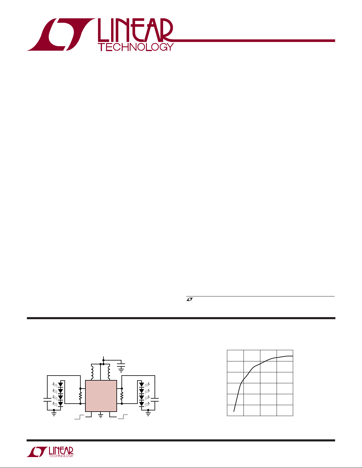
TYPICAL APPLICATION
Li-Ion Power Driver for 4/4 White LEDs
V
IN
3V TO 5V
1µF
15µH
SW1 V
CAP1 CAP2
LED1 LED2
CTRL1
OFF ON
SHUTDOWN
AND DIMMING
CONTROL 1
IN
LT3497
GND
15µH
SW2
CTRL2
SHUTDOWN
AND DIMMING
CONTROL 2
OFF ON
Effi ciency
80
= 3.6V
V
IN
4/4LEDs
1µF
10Ω10Ω
1µF
3497 TA01a
75
70
65
EFFICIENCY (%)
60
55
50
0
5101520
LED CURRENT (mA)
3497 TA01b
3497f
1
LT3497
(Note 1)
Input Voltage (VIN) ...................................................10V
SW1, SW2 Voltages ..................................................35V
CAP1, CAP2 Voltages ................................................35V
CTRL1, CTRL2 Voltages ............................................10V
LED1, LED2 Voltages ................................................35V
Operating Temperature Range ................. –40°C to 85°C
Maximum Junction Temperature .......................... 125°C
Storage Temperature Range ...................–65°C to 125°C
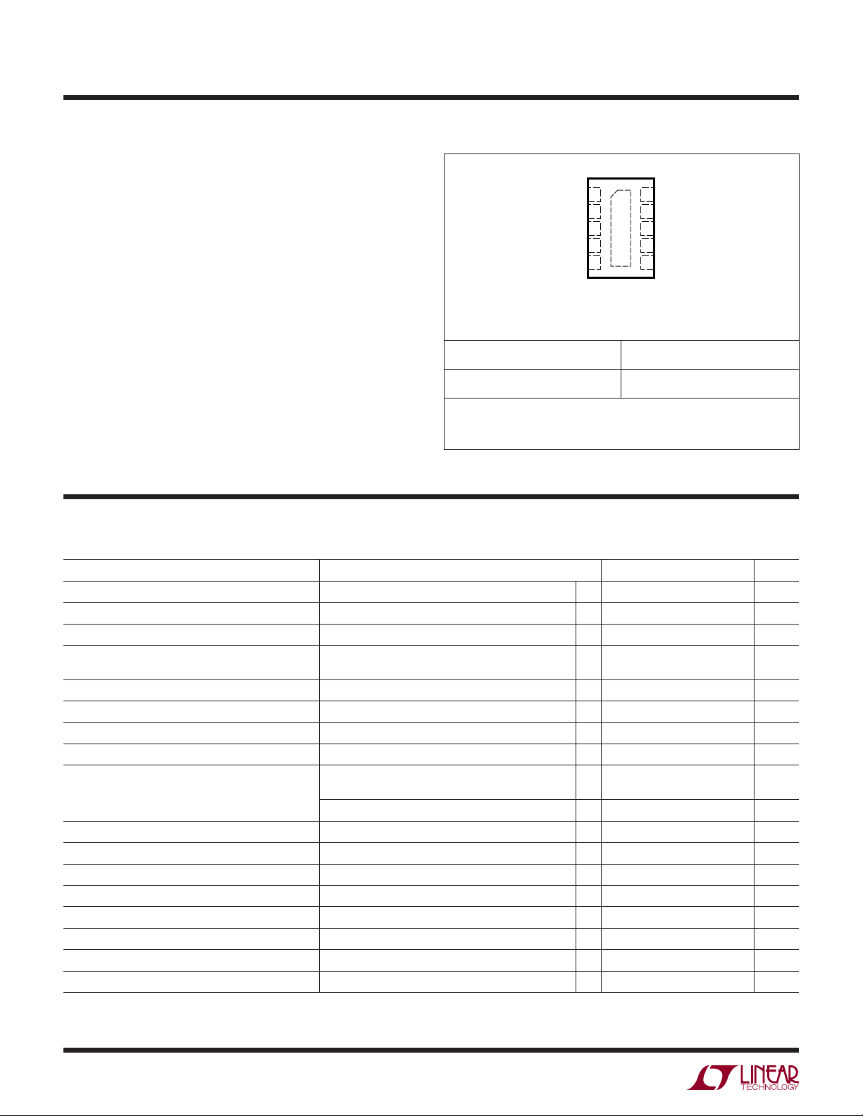
PACKAGE/ORDER INFORMATIONABSOLUTE MAXIMUM RATINGS
TOP VIEW
1
LED1
2
CTRL1
3
GND
4
CTRL2
5
LED2
10-LEAD (3mm × 2mm) PLASTIC DFN
T
JMAX
EXPOSED PAD (PIN 11) IS GND, MUST BE SOLDERED TO PCB
DDB PACKAGE
= 125°C, θJA = 76°C/W, θJC = 13.5°C/W
ORDER PART NUMBER DDB PART MARKING
LT3497EDDB LCGT
Order Options Tape and Reel: Add #TR
Lead Free: Add #PBF Lead Free Tape and Reel: Add #TRPBF
Lead Free Part Marking: http://www.linear.com/leadfree/
Consult LTC Marketing for parts specifi ed with wider operating temperature ranges.
10
CAP1
9
SW1
11
8
V
IN
7
SW2
6
CAP2
ELECTRICAL CHARACTERISTICS
The
temperature range, otherwise specifi cations are at T
= 25°C. VIN = 3V, V
A
●
denotes the specifi cations which apply over the full operating
CTRL1
= V
CTRL2
= 3V.
PARAMETER CONDITIONS MIN TYP MAX UNITS
Minimum Operating Voltage 2.5 V
– V
LED Current Sense Voltage (V
LED Current Sense Voltage (V
LED1
) Between
OS
) – (V
CAP2
– V
Offset Voltage (V
(V
– V
CAP1
CAP1
CAP2
LED2
) Voltages
)V
LED1
– V
)V
LED2
CAP1, LED1 Pin Bias Current V
CAP2, LED2 Pin Bias Current V
, V
V
V
CAP1
CAP2
Common Mode Minimum Voltage 2.5 V
LED1
, V
Common Mode Minimum Voltage 2.5 V
LED2
Supply Current V
CAP1
CAP2
V
OS
CAP1
CAP2
CAP1
V
CTRL1
V
CTRL1
= 16V
= 16V
= |(V
= 16V, V
= 16V, V
= V
= V
= V
– V
CAP1
CAP2
CTRL2
CTRL2
) – (V
LED1
= 16V 20 40 µA
LED1
= 16V 20 40 µA
LED2
= 16V, V
= 3V
= 0V 12 18 µA
LED1
CAP2
= V
– V
)| 0 2 8 mV
LED2
= 15V,
LED2
●
190 200 210 mV
●
190 200 210 mV
6 8.5 mA
Switching Frequency 1.8 2.3 2.8 MHz
Maximum Duty Cycle 88 92 %
●
Converter 1 Switch Current Limit SW1
Converter 2 Switch Current Limit SW2
Converter 1 V
Converter 2 V
CESAT
CESAT
Switch 1 Leakage Current V
Switch 2 Leakage Current V
I
= 200mA 200 mV
SW1
I
= 200mA 200 mV
SW2
= 16V 0.1 5 µA
SW1
= 16V 0.1 5 µA
SW2
300 400 mA
●
300 400 mA
2
3497f
LT3497
ELECTRICAL CHARACTERISTICS
The
temperature range, otherwise specifi cations are at T
PARAMETER CONDITIONS MIN TYP MAX UNITS
Voltage for Full LED Current V
V
CTRL1
Voltage for Full LED Current V
V
CTRL2
or V
V
CTRL1
and V
V
CTRL1
CTRL1, CTRL2 Pin Bias Current 100 nA
CAP1 Pin Overvoltage Protection
CAP2 Pin Overvoltage Protection
Schottky 1 Forward Drop I
Schottky 2 Forward Drop I
Schottky 1 Reverse Leakage Current V
Schottky 2 Reverse Leakage Current V
Note 1: Stresses beyond those listed under Absolute Maximum Ratings
may cause permanent damage to the device. Exposure to any Absolute
Maximum Rating condition for extended periods may affect device
reliability and lifetime.
Voltage to Turn On the IC
CTRL2
Voltages to Shut Down the IC 50 mV
CTRL2
= 25°C. VIN = 3V, V
A
= 16V
CAP1
= 16V
CAP2
SCHOTTKY1
SCHOTTKY2
= 25V 4 µA
R1
= 25V 4 µA
R2
●
denotes the specifi cations which apply over the full operating
= V
CTRL1
= 100mA 0.8 V
= 100mA 0.8 V
Note 2: The LT3497E is guaranteed to meet performance specifi cations
from 0°C to 85°C. Specifi cations over the –40°C to 85°C operating
temperature range are assured by design, characterization and correlation
with statistical process controls.
CTRL2
= 3V.
●
1.5 V
●
1.5 V
●
100 mV
●
30 32 34 V
●
30 32 34 V
3497f
3
LT3497
TYPICAL PERFORMANCE CHARACTERISTICS
= 25°C unless otherwise specifi ed)
(T
A
Switch Saturation Voltage
(V
)
CESAT
450
400
350
300
250
200
150
100
SWITCH SATURATION VOLTAGE (mV)
50
0
50
0
100
SWITCH CURRENT (mA)
Sense Voltage (V
vs V
240
200
160
120
SENSE VOLTAGE (mV)
CTRL
80
40
150
–50°C
–50°C
125°C
200
CAP
25°C
125°C
250
– V
300
LED
25°C
)
350
3497 G01
Schottky Forward Voltage Drop
400
350
300
250
200
150
100
50
SCHOTTKY FORWARD CURRENT (mA)
400
0
0
SCOTTKY FORWARD DROP (mV)
Open-Circuit Output Clamp
Voltage
34
33
32
31
OUTPUT CLAMP VOLTAGE (V)
125°C
25°C
–50°C
200 400 800
25°C
600
–50°C
125°C
3497 G02
1000
Shutdown Current
= V
(V
CTRL1
15
12
9
6
SHUTDOWN CURRENT (µA)
3
0
2
0
CTRL2
4
VIN (V)
= 0V)
–50°C
Input Current in Output Open
Circuit
30
25
150°C
20
15
10
INPUT CURRENT (mA)
5
–50°C
6
25°C
125°C
25°C
8
10
3497 G03
4
0
0
500 1000 1500 2000
V
(mV)
CTRL
3497 G04
30
2
0
4
VIN (V)
6
8
10
3497 G05
0
2
46 810
VIN (V)
3497 G06
Switching Waveform Transient Response
V
V
SW
10V/DIV
V
CAP
50mV/DIV
100mA/DIV
I
L
VIN = 3.6V
FRONT PAGE
APPLICATION CIRCUIT
200ms/DIV
3497 G07
CAP
5V/DIV
V
CTRL
5V/DIV
200mA/DIV
I
L
VIN = 3.6V
FRONT PAGE
APPLICATION CIRCUIT
1ms/DIV
3497 G08
3497f
TYPICAL PERFORMANCE CHARACTERISTICS
Quiescent Current Current Limit vs Temperature
7
6
5
4
3
2
QUIESCENT CURRENT (mA)
1
0
246 10
0
125°C
25°C
–50°C
8
VIN (V)
3497 G09
500
450
400
CURRENT LIMIT (mA)
350
300
–50
–25 0 25 50
TEMPERATURE (°C)
75 100 125
= 25°C unless otherwise specifi ed)
(T
A
Schottky Leakage Current vs
Temperature (–50°C to 125°C)
3
2
1
SCHOTTKY LEAKAGE CURRENT (µA)
0
–50 –25 0 25 50
3497 G11
TEMPERATURE (°C)
LT3497
24V
16V
75 100 125
3497 G12
Open-Circuit Output Clamp Voltage
vs Temperature (–50°C to 125°C)
36
34
32
30
OUTPUT CLAMP VOLTAGE (V)
28
–50
–25 0 25 50
TEMPERATURE (°C)
75 100 125
Sense Voltage (V
vs V
CAP
208
204
3497 G13
INPUT CURRENT (mA)
– V
CAP
LED
Input Current in Output Open
Circuit vs Temperature
(–50°C to 125°C)
30
VIN = 3V
25
20
15
10
5
0
–50
–25 0
TEMPERATURE (°C)
50 100 125
25 75
)
Switching Frequency vs
Temperature
2.60
VIN = 3.6V
2.50
2.40
2.30
2.20
2.10
2.00
SWITCHING FREQUENCY (MHz)
1.90
1.80
–25 0 50
–50
3497 G14
Sense Voltage vs Temperature
206
202
25
TEMPERATURE (°C)
75 100 125
3497 G15
200
196
SENSE VOLTAGE (mV)
192
188
10
5
15
125°C
–50°C
V
CAP
(V)
25°C
20
25
30
3497 G16
198
SENSE VOLTAGE (mV)
194
190
–50
–25 0 25 50
TEMPERATURE (°C)
75 100 125
3497 G17
3497f
5

LT3497
PIN FUNCTIONS
LED1 (Pin 1): Connection point for the anode of the fi rst
LED of the fi rst set of LEDs and the sense resistor (R
SENSE1
).
The LED current can be programmed by:
200
mV
=
I
LED
R
SENSE11
CTRL1 (Pin 2): Dimming and Shutdown Pin. Connect
CTRL1 below 50mV to disable converter 1. As the pin voltage is ramped from 0V to 1.5V, the LED current ramps from
0 to (I
= 200mV/R
LED1
). The CTRL1 pin must not
SENSE1
be left fl oating.
GND (Pin 3): Connect the GND pin to the PCB system
ground plane.
CTRL2 (Pin 4): Dimming and Shutdown Pin. Connect
CTRL2 below 50mV to disable converter 2. As the pin voltage is ramped from 0V to 1.5V, the LED current ramps from
0 to (I
= 200mV/R
LED2
). The CTRL2 pin must not
SENSE2
be left fl oating.
LED2 (Pin 5): Connection point for the anode of the fi rst
LED of the second set of LEDs and the sense resistor
(R
). The LED current can be programmed by:
SENSE2
CAP2 (Pin 6): Output of Converter 2. This pin is connected
to the cathode of internal Schottky diode 2. Connect the
output capacitor to this pin and the sense resistor (R
SENSE2
)
from this pin to LED2 pin.
SW2 (Pin 7): Switch Pin. Minimize trace area at this pin
to minimize EMI. Connect the inductor at this pin.
(Pin 8): Input Supply Pin. This pin must be locally
V
IN
bypassed.
SW1 (Pin 9): Switch Pin. Minimize trace area at this pin
to minimize EMI. Connect the inductor at this pin.
CAP1 (Pin 10): Output of Converter 1. This pin is connected
to the cathode of internal Schottky diode 1. Connect the
output capacitor to this pin and the sense resistor (R
SENSE1
)
from this pin to LED1 pin.
Exposed Pad (Pin 11): Ground. Must be soldered to
PCB.
200
mV
=
I
LED
R
SENSE22
6
3497f

BLOCK DIAGRAM
LT3497
OUT2
1µF
C
SENSE2
R
10Ω
6
5
3497 F01
+
+
LED2
R
–
A3
RAMP
GENERATOR
A3
–
R
2.3MHz
OSCILLATOR
CONVERTER 1 CONVERTER 2
+
AMP
AMP g
g
+
m
m
–
A = 6.25
–
+
A1
A11.25V 1.25V
–
+
A = 6.25
–
4
+
C
C
C
R
3
GND
C
C
C
R
Figure 1. LT3497 Block Diagram
+
CTRL1 CTRL2
2
START-UP START-UP
CAP2
PROTECT
SW2
7
L2
15µH
IN
8
V
CIN1µF
L1
15µH
SW1
9
OVERVOLTAGE
DRIVERDRIVER
–
–
Q2
Q
R
S
R
A2
+
+
A2
R
S
R
Q
Q1
PROTECT
OVERVOLTAGE
CAP1
10
10Ω
SENSE1
R
LED1
1
OUT1
C
1µF
3497f
7

LT3497
OPERATION
Main Control Loop
The LT3497 uses a constant frequency, current mode control scheme to provide excellent line and load regulation.
It incorporates two identical, but fully independent PWM
converters. Operation can be best understood by referring
to the Block Diagram in Figure 1. The oscillator, start-up
bias and the band gap reference are shared between the two
converters. The control circuitry, power switch, Schottky
diode etc., are identical for both the converters.
At power up, the capacitors at CAP1 and CAP2 pins are
charged up to V
(input supply voltage) via their respective
IN
inductor and the internal Schottky diode. If either CTRL1
and CTRL2 or both are pulled higher than 100mV, the
bandgap reference, the start-up bias and the oscillator
are turned on.
The main control loop can be understood by following the
operation of converter 1. At the start of each oscillator cycle,
the power switch, Q1, is turned on. A voltage proportional
to the switch current is added to a stabilizing ramp and the
resulting sum is fed into the positive terminal of the PWM
comparator, A2. When this voltage exceeds the level at the
negative input of A2, the PWM logic turns off the power
switch. The level at the negative input of A2 is set by the
error amplifi er, A1, and is simply an amplifi ed version of
the difference between the V
CAP1
and V
voltage and
LED1
the bandgap reference. In this manner the error amplifi er,
A1, sets the correct peak current level in inductor L1 to
keep the output in regulation. The CTRL1 pin is used to
adjust the LED current.
If only one of the converters is turned on, the other converter
will stay off and its output will remain charged up to V
IN
(input supply voltage). The LT3497 enters into shutdown
when both CTRL1 and CTRL2 pins are pulled lower than
50mV. The CTRL1 and CTRL2 pins perform independent
dimming and shutdown control for the two converters.
Minimum Output Current
The LT3497 can drive a 4-LED string at 2mA LED current
without pulse skipping. As current is further reduced, the
device may begin skipping pulses.
This will result in some low frequency ripple, although the
average LED current remains regulated down to zero. The
photo in Figure 2 details circuit operation driving 4 white
LEDs at 2mA. Peak inductor current is less than 50mA and
the regulator operates in discontinuous mode, meaning
the inductor current reaches zero during the discharge
phase. After the inductor current reaches zero, the SW
pin exhibits ringing due to the LC tank circuit formed
by the inductor in combination with the switch and the
diode capacitance. This ringing is not harmful; far less
spectral energy is contained in the ringing than in the
switch transitions.
8
50mA/DIV
V
SW
10V/DIV
I
L
V
= 4.2V
IN
= 2mA
I
LED
4 LEDs
Figure 2. Switching Waveforms
200ns/DIV
3497 F02
3497f

APPLICATIONS INFORMATION
LT3497
DUTY CYCLE
The duty cycle for a step-up converter is given by:
VVV
++–
D
OUT D IN
=
VVV
OUT D CESAT
–
where:
V
V
V
V
= Output voltage
OUT
= Schottky forward voltage drop
D
= Saturation voltage of the switch
CESAT
= Input voltage
IN
The maximum duty cycle achievable for LT3497 is 88%
when running at 2.3MHz switching frequency. Always
ensure that the converter is not duty-cycle limited when
powering the LEDs at a given frequency.
INDUCTOR SELECTION
A 15µH inductor is recommended for most LT3497 applications. Although small size and high effi ciency are
major concerns, the inductor should have low core losses
at 2.3MHz and low DCR (copper wire resistance). Some
inductors in this category with small size are listed in
Table 1. The effi ciency comparison of different inductors
is shown in Figure 3.
Table 1: Recommended Inductors
MAX
DCR
(Ω)
0.58
1.6
0.3
1.2
CURRENT
RATING
(mA) VENDOR
300
Murata
200
www.murata.com
450
225
www.cooperet.com
www.toko.com
www.sumida.com
PART
LQH32CN150K53
LQH2MCN150K02
LQH32CN100K53
LQH2MCN100K02
SD3112-150 15 0.654 440 Cooper
1001AS-150M
(TYPE D312C)
CDRH2D11/HP 15 0.739 410 Sumida
L
(µH)
15
15
10
10
15 0.80 360 Toko
CAPACITOR SELECTION
The small size of ceramic capacitors make them ideal for
LT3497 applications. Use only X5R and X7R types because
they retain their capacitance over wider temperature ranges
than other types such as Y5V or Z5U. A 1µF input capacitor
15µH MURATA LQH32CN150K53
15µH MURATA LQH2MCN150K02
15µH COOPER SD3112-150
15µH TOKO 1001AS-150M TYPE D312C
80
75
70
65
60
EFFICIENCY (%)
55
50
45
Figure 3. Effi ciency Comparison of Different Inductors
15µH SUMIDA CDRH2D11/HP
0
510 20
LED CURRENT (mA)
15
3497 F03
and a 1µF output capacitor are suffi cient for most applications. Table 2 shows a list of several ceramic capacitor
manufacturers. Consult the manufacturers for detailed
information on their entire selection of ceramic parts.
Table 2: Recommended Ceramic Capacitor Manufacturers
Taiyo Yuden (800) 368-2496
AVX (803) 448-9411
Murata (714) 852-2001
www.t-yuden.com
www.avxcorp.com
www.murata.com
OVERVOLTAGE PROTECTION
The LT3497 has an internal open-circuit protection
circuit for both converters. In the cases of output open
circuit, when the LEDs are disconnected from the circuit
or the LEDs fail open circuit, the converter V
voltage
CAP
is clamped at 32V (typ). Figure 4a shows the transient
response of the front page application step-up converter
with LED1 disconnected. With LED1 disconnected, the
converter starts switching at the peak inductor current
limit. The converter output starts ramping up and fi nally
gets clamped at 32V (typ). The converter will then switch
at low inductor current to regulate the converter output
at the clamp voltage. The V
and input current during
CAP
output open circuit are shown in the Typical Performance
Characteristics.
3497f
9

LT3497
APPLICATIONS INFORMATION
V
CAP
10V/DIV
I
SW
200mA/DIV
= 3.6V
V
IN
FRONT PAGE
APPLICATION CIRCUIT
Figure 4a. Transient Response of Switcher 1 with LED1
Disconnected from the Output
I
L1
50mA/DIV
V
SW1
20V/DIV
I
L2
50mA/DIV
V
SW2
20V/DIV
V
= 3.6V
IN
4 LEDs
LED 2 DISCONNECTED
500µs/DIV
LEDs DISCONNECTED
AT THIS INSTANT
200ms/DIV
3497 F04a
3497 F04b
For low DCR inductors, which are usually the case for this
application, the peak inrush current can be simplifi ed as
follows:
r
α
=
2
•
L
=
=
1
•
LC
V
IN
L
ω
I
PK
–
06
–.
ω
•
4
2
r
2
•
L
αωπ
⎛
• exp – •
⎜
⎝
⎞
⎟
⎠
22
where L is the inductance, r is the DCR of the inductor
and C is the output capacitance.
Table 3 gives inrush peak currents for some component
selections.
Table 3: Inrush Peak Currents
VIN (V) r (Ω)L (µH)C
4.2 0.58 15 1 0.828
4.2 1.6 15 1 0.682
4.2 0.8 15 1 0.794
4.2 0.739 15 1 0.803
(µF) IP (A)
OUT
Figure 4b. Switching Waveforms with Output 1 Open Circuit
In the event one of the converters has an output open
circuit, its output voltage will be clamped at 32V. However,
the other converter will continue functioning properly.
The photo in Figure 4b shows circuit operation with
converter 2 output open circuit and converter 1 driving
4 LEDs at 20mA. Converter 2 starts switching at a lower
peak inductor current and begins skipping pulses, thereby
reducing its input current.
INRUSH CURRENT
The LT3497 has built-in Schottky diodes. When supply
voltage is applied to the V
pin, an inrush current fl ows
IN
through the inductor and the Schottky diode and charges
up the CAP voltage. Both the Schottky diodes in the LT3497
can sustain a maximum current of 1A. The selection of
inductor and capacitor value should ensure the peak of
the inrush current to be below 1A.
PROGRAMMING LED CURRENT
The LED current of each LED string can be set independently by the choice of resistors R
SENSE1
and R
SENSE2
,
respectively. For each LED string, the feedback resistor
(R
) and the sense voltage (V
SENSE
CAP
– V
) control the
LED
LED current.
For each independent LED string, the CTRL pin controls
the sense reference voltage as shown in the Typical
Performance Characteristics. For CTRL higher than 1.5V,
the sense reference is 200mV, which results in full LED
current. In order to have accurate LED current, precision
resistors are preferred (1% is recommended). The formula
and Table 4 for R
R
SENSE
200
=
I
LED
selection are shown below.
SENSE
mV
3497f
10

APPLICATIONS INFORMATION
LT3497
Table 4: R
Value Selection for 200mV Sense
SENSE
I
(mA) R
LED
540
10 20
15 13.3
20 10
SENSE
(Ω)
DIMMING CONTROL
There are three different types of dimming control circuits.
The LED current can be set by modulating the CTRL pin
with a DC voltage, a fi ltered PWM signal or directly with
a PWM signal.
Using a DC Voltage
For some applications, the preferred method of brightness
control is a variable DC voltage to adjust the LED current.
The CTRL pin voltage can be modulated to set the dimming of the LED string. As the voltage on the CTRL pin
increases from 0V to 1.5V, the LED current increases from
0 to I
. As the CTRL pin voltage increases beyond 1.5V,
LED
it has no effect on the LED current.
The LED current can be set by:
200
I
I
mV
≈>
LED
LED
≈
R
SENSE
.. •.25
V
CTRL
SENSE
CTRL
when V
156.when V
CTRL
V
<
125RV
Feedback voltage variation versus control voltage is given
in the Typical Performance Characteristics.
Using a Filtered PWM Signal
A fi ltered PWM can be used to control the brightness of
the LED string. The PWM signal is fi ltered (Figure 5) by a
RC network and fed to the CTRL1, CTRL2 pins.
The corner frequency of R1, C1 should be much lower
than the frequency of the PWM signal. R1 needs to be
much smaller than the internal impedance in the CTRL
pins which is 10MΩ (typ).
C1
0.1µF
LT3497
CTRL1,2
3497 F05
R1
100k
PWM
10kHz TYP
Figure 5. Dimming Control Using a Filtered PWM Signal
Direct PWM Dimming
Changing the forward current fl owing in the LEDs not only
changes the intensity of the LEDs, it also changes the color.
The chromaticity of the LEDs changes with the change in
forward current. Many applications cannot tolerate any
shift in the color of the LEDs. Controlling the intensity of
the LEDs with a direct PWM signal allows dimming of the
LEDs without changing the color. In addition, direct PWM
dimming offers a wider dimming range to the user.
Dimming the LEDs via a PWM signal essentially involves
turning the LEDs on and off at the PWM frequency. The
typical human eye has a limit of ~60 frames per second.
By increasing the PWM frequency to ~80Hz or higher,
the eye will interpret that the pulsed light source is continuously on. Additionally, by modulating the duty cycle
(amount of “on time”) the intensity of the LEDs can be
controlled. The color of the LEDs remains unchanged in
this scheme since the LED current value is either zero or
a constant value.
Figure 6 shows a Li-ion powered 4/4 white LED driver. Direct
PWM dimming method requires an external NMOS tied
between the cathode of the lowest LED in the string and
ground as shown in Figure 6. Si2318DS MOSFETs can be
used since its sources are connected to ground. The PWM
signal is applied to the (CTRL1 and CTRL2) control pins of
the LT3497 and the gate of the MOSFET. The PWM signal
should traverse between 0V to 5V to ensure proper turn
on and off of the converters and the NMOS transistors (Q1
and Q2). When the PWM signal goes high, LEDs are connected to ground and a current of I
LED
= (200mV/R
SENSE
)
fl ows through the LEDs. When the PWM signal goes low,
the LEDs are disconnected and turn off. The low PWM
input applied to the LT3497 ensures that the respective
3497f
11

LT3497
APPLICATIONS INFORMATION
converter turns off. The MOSFETs ensure that the LEDs
quickly turn off without discharging the output capacitors
which in turn allows the LEDs to turn on faster. Figures 7
and 8 show the PWM dimming waveforms and effi ciency
for the Figure 6 circuit.
The time it takes for the LEDs current to reach its programmed value sets the achievable dimming range for a
given PWM frequency. For example, the settling time of
the LEDs current in Figure 7 is approximately 40μs for a
3V input voltage. The achievable dimming range for this
application and 100Hz PWM frequency can be determined
using the following method.
3V TO 5V
L1
15µH
SW1 V
IN
CAP1 CAP2
R
1µF
Si2318DS
SENSE1
10Ω
Q1
100k 100k
LT3497
LED1 LED2
CTRL1 CTRL2
GND
5V
0V
PWM
FREQ
Example:
ƒ = 100Hz, t
t
PERIOD
= 1/ƒ = 1/100 = 0.01s
Dim Range = t
Min Duty Cycle = t
= 40μs
SETTLE
PERIOD/tSETTLE
SETTLE/tPERIOD
= 0.01s/40μs = 250:1
• 100
= 40μs/0.01s = 0.4%
Duty Cycle Range = 100%→0.4% at 100Hz
The calculations show that for a 100Hz signal the dimming
range is 250 to 1. In addition, the minimum PWM duty
cycle of 0.4% ensures that the LEDs current has enough
1µF
L2
15µH
SW2
R
SENSE2
PWM
FREQ
10Ω
Q2
Si2318DS
5V
0V
1µF
3497 F06
I
LED
20mA/DIV
200mA/DIV
PWM
5V/DIV
12
Figure 6. Li-Ion to 4/4 White LEDs with Direct PWM Dimming
I
L
= 3.6V
V
IN
4 LEDs
2ms/DIV
Figure 7. Direct PWM Dimming Waveforms
3497 F07
80
= 3.6V
V
IN
4/4 LEDs
78
76
74
EFFICIENCY (%)
72
70
0
5
10
LED CURRENT (mA)
Figure 8. Effi ciency
15
20
3497 F08
3497f

APPLICATIONS INFORMATION
LT3497
time to settle to its fi nal value. Figure 9 shows the available dimming range for different PWM frequencies with
a settling time of 40μs.
10000
1000
100
PWM DIMMING RANGE
10
1
10
PULSING MAY BE VISIBLE
100 1000 10000
PWM FREQUENCY (Hz)
3497 F09
Figure 9. Dimming Ratio vs Frequency
The dimming range can be further extended by changing
the amplitude of the PWM signal. The height of the PWM
signal sets the commanded sense voltage across the sense
resistor through the CTRL pin. In this manner both analog
dimming and direct PWM dimming extend the dimming
range for a given application. The color of the LEDs no
longer remains constant because the forward current of
the LED changes with the height of the CTRL signal. For
the 4-LED application described above, the LEDs can be
dimmed fi rst, modulating the duty cycle of the PWM signal.
Once the minimum duty cycle is reached, the height of the
PWM signal can be decreased below 1.5V down to 100mV.
The use of both techniques together allows the average LED
current for the 4-LED application to be varied from 20mA
down to less than 20µA. Figure 10 shows the application
for dimming using both analog dimming and PWM dimming. A potentiometer must be added to ensure that the
gate of the NMOS receives a logic-level signal, while the
CTRL signal can be adjusted to lower amplitudes.
LOW INPUT VOLTAGE APPLICATIONS
The LT3497 can be used in low input voltage applications. The input supply voltage to the LT3497 must be
2.5V or higher. However, the inductors can be run off a
3V TO 5V
1µF
GND
L2
15µH
SW2
IN
R
PWM
FREQ
SENSE2
10Ω
5V
0V
1µF
Q2
Si2318DS
3497 F10
1µF
Si2318DS
L1
15µH
SW1 V
CAP1 CAP2
R
SENSE1
10Ω
5V
0V
PWM
Q1
FREQ
100k 100k
LT3497
LED1 LED2
CTRL1 CTRL2
Figure 10. Li-Ion to 4/4 White LEDs with Both PWM Dimming
and Analog Dimming
lower battery voltage. This technique allows the LEDs to
be powered off two alkaline cells. Most portable devices
have a 3.3V supply voltage which can be used to power
the LT3497. The LEDs can be driven straight from the
battery, resulting in higher effi ciency.
Figure 11 shows 3/3 LEDs powered by two AA cells.
The battery is connected to the inductors and the chip is
powered off a 3.3V logic supply voltage.
3.3V
2 AA CELLS
2V TO 3.2V
C3
1µF
C1
1µF
R
SENSE1
L1
15µH
SW1 V
CAP1 CAP2
10Ω
LED1 LED2
CTRL1
OFF ON
SHUTDOWN
AND DIMMING
CONTROL 1
C1, C2: TAIYO YUDEN LMK212BJ105MG
C3, C4: TAIYO YUDEN GMK212BJ105KG
L1, L2: MURATA LQH32CN150K53
IN
LT3497
GND
SW2
CTRL2
SHUTDOWN
AND DIMMING
CONTROL 2
Figure 11. 2 AA Cells to 3/3 White LEDs
L2
15µH
OFF ON
C2
1µF
R
SENSE2
10Ω
C4
1µF
3497 F11
3497f
13

LT3497
APPLICATIONS INFORMATION
BOARD LAYOUT CONSIDERATIONS
As with all switching regulators, careful attention must be
paid to the PCB board layout and component placement.
To prevent electromagnetic interference (EMI) problems,
proper layout of high frequency switching paths is essential.
Minimize the length and area of all traces connected to
the switching node pins (SW1 and SW2). Keep the sense
voltage pins (CAP1, CAP2, LED1 and LED2) away from
VIA TO
GROUND PLANE
C
OUT2
CAP2
10
9
V
IN
8
7
6
CAP1
VIA TO
GROUND
PLANE
SW2
L2
C
L1
SW1
IN
C
OUT1
the switching node. Place the output capacitors (C
and C
The placement of a bypass capacitor on V
) next to the output pins (CAP1 and CAP2).
OUT2
needs to be
IN
OUT1
in close proximity to the IC to fi lter EMI noise from SW1
and SW2. Always use a ground plane under the switching
regulator to minimize interplane coupling. Recommended
component placement is shown in Figure 12.
LED2
5
4
3
2
1
LED1
GND
CTRL2
CTRL1
3497 F12
TYPICAL APPLICATIONS
Li-Ion to 1/2 White LEDs
V
IN
3V TO 5V
C1
R
SENSE1
1µF
L1
10µH
SW1 V
CAP1 CAP2
10Ω
OFF ON
SHUTDOWN
AND DIMMING
CONTROL 1
C1, C2: TAIYO YUDEN GMK212BJ105KG
C3: TAIYO YUDEN LMK212BJ105MG
L1, L2: MURATA LQH32CN100K53
LT3497
LED1 LED2
CTRL1
IN
GND
L2
10µH
SW2
CTRL2
OFF ON
SHUTDOWN
AND DIMMING
CONTROL 2
VIAS TO
GROUND PLANE
Figure 12. Recommended Component Placement
Conversion Effi ciency
70
VIN = 3.6V
1/2LEDs
65
60
55
50
45
EFFICIENCY (%)
40
35
30
0
C2
1µF
R
SENSE2
10Ω
3497 TA02a
C3
1µF
10
5
LED CURRENT (mA)
15
20
3497 TA02b
3497f
14

TYPICAL APPLICATIONS
Li-Ion to 2/2 White LEDs
LT3497
C1
R
SENSE1
1µF
L1
10µH
SW1 V
CAP1 CAP2
10Ω
OFF ON
SHUTDOWN
AND DIMMING
CONTROL 1
C1, C2: TAIYO YUDEN GMK212BJ105KG
C3: TAIYO YUDEN LMK212BJ105MG
L1, L2: MURATA LQH32CN100K53
LT3497
LED1 LED2
CTRL1
Li-Ion to 2/2 White LEDs
L1
10µH
SW1 V
CAP1 CAP2
C1
R
SENSE1
1µF
10Ω
OFF ON
SHUTDOWN
AND DIMMING
CONTROL 1
C1, C2: TAIYO YUDEN GMK212BJ105KG
C3: TAIYO YUDEN LMK212BJ105MG
L1, L2: MURATA LQH32CN100K53
LT3497
LED1 LED2
CTRL1 CTRL2
V
IN
3V TO 5V
IN
CTRL2
GND
3V TO 5V
IN
GND
L2
10µH
SW2
OFF ON
SHUTDOWN
AND DIMMING
CONTROL 2
L2
10µH
SW2
R
SENSE2
OFF ON
SHUTDOWN
AND DIMMING
CONTROL 2
C2
1µF
R
SENSE2
10Ω
C3
1µF
10Ω
3497 TA12a
3497TA13a
C2
1µF
C3
1µF
70
VIN = 3.6V
2/2 LEDs
65
60
55
EFFICIENCY (%)
50
45
40
0
80
V
= 3.6V
IN
2/2LEDs
75
70
65
60
55
EFFICIENCY (%)
50
45
40
0
Conversion Effi ciency
5101520
LED CURRENT (mA)
3497 TA12b
Conversion Effi ciency
5
10
LED CURRENT (mA)
15
20
3497 TA13b
3497f
15

LT3497
TYPICAL APPLICATIONS
Li-Ion to 2/4 White LEDs
V
IN
3V TO 5V
C1
R
SENSE1
1µF
L1
10µH
SW1 V
CAP1 CAP2
10Ω
OFF ON
SHUTDOWN
AND DIMMING
CONTROL 1
C1, C2: TAIYO YUDEN GMK212BJ105KG
C3: TAIYO YUDEN LMK212BJ105MG
L1: MURATA LQH32CN100K53
L2: MURATA LQH32CN150K53
LT3497
LED1 LED2
CTRL1
IN
GND
L2
15µH
SW2
CTRL2
OFF ON
SHUTDOWN
AND DIMMING
CONTROL 2
C3
1µF
R
SENSE2
10Ω
3497 TA03a
C2
1µF
80
VIN = 3.6V
2/4LEDs
75
70
65
60
EFFICIENCY (%)
55
50
45
0
Conversion Effi ciency
510 20
LED CURRENT (mA)
15
3497 TA03b
1µF
Li-Ion to 3/3 White LEDs
V
IN
3V TO 5V
C3
L1
15µH
SW1 V
C1
R
SENSE1
CAP1 CAP2
10Ω
LED1 LED2
CTRL1
OFF ON
SHUTDOWN
AND DIMMING
CONTROL 1
C1, C2: TAIYO YUDEN GMK212BJ105KG
C3: TAIYO YUDEN LMK212BJ105MG
L1, L2: MURATA LQH32CN150K53
IN
LT3497
GND
SW2
CTRL2
SHUTDOWN
AND DIMMING
L2
15µH
OFF ON
CONTROL 2
1µF
R
SENSE2
10Ω
C2
1µF
3497 TA04a
80
75
70
65
60
EFFICIENCY (%)
55
50
45
Conversion Effi ciency
VIN = 3.6V
3/3LEDs
0
510 20
LED CURRENT (mA)
15
3497 TA04b
16
3497f

TYPICAL APPLICATIONS
Li-Ion to 4/6 White LEDs
LT3497
1µF
V
IN
3V TO 5V
C3
L1
15µH
SW1 V
C1
R
SENSE1
CAP1 CAP2
10Ω
LED1 LED2
CTRL1
OFF ON
SHUTDOWN
AND DIMMING
CONTROL 1
C1, C2: TAIYO YUDEN GMK212BJ105KG
C3: TAIYO YUDEN LMK212BJ105MG
L1, L2: MURATA LQH32CN150K53
IN
LT3497
GND
SW2
CTRL2
SHUTDOWN
AND DIMMING
L2
15µH
OFF ON
CONTROL 2
1µF
R
SENSE2
10Ω
C2
1µF
3497 TA05a
80
75
70
65
EFFICIENCY (%)
60
55
50
Conversion Effi ciency
= 3.6V
V
IN
4/6LEDs
0
5101520
LED CURRENT (mA)
3497 TA05b
Li-Ion to 5/5 White LEDs
1µF
V
IN
3V TO 5V
C3
L1
15µH
SW1 V
C1
R
SENSE1
CAP1 CAP2
10Ω
LED1 LED2
CTRL1
OFF ON
SHUTDOWN
AND DIMMING
CONTROL 1
C1, C2: TAIYO YUDEN GMK212BJ105KG
C3: TAIYO YUDEN LMK212BJ105MG
L1, L2: MURATA LQH32CN150K53
IN
LT3497
GND
SW2
CTRL2
SHUTDOWN
AND DIMMING
L2
15µH
OFF ON
CONTROL 2
1µF
R
SENSE2
10Ω
C2
1µF
3497 TA06a
80
75
70
65
EFFICIENCY (%)
60
55
50
Conversion Effi ciency
= 3.6V
V
IN
5/5LEDs
0
5101520
LED CURRENT (mA)
3497 TA06b
3497f
17

LT3497
TYPICAL APPLICATIONS
Li-Ion to 6/6 White LEDs
V
IN
3V TO 5V
L1
15µH
L2
15µH
C3
1µF
80
75
Conversion Effi ciency
= 3.6V
V
IN
6/6LEDs
1µF
SW1 V
CAP1 CAP2
R
C1
SENSE1
10Ω
LED1 LED2
CTRL1
OFF ON
SHUTDOWN
AND DIMMING
CONTROL 1
C1, C2: TAIYO YUDEN GMK212BJ105KG
C3: TAIYO YUDEN LMK212BJ105MG
L1, L2: MURATA LQH32CN150K53
IN
LT3497
GND
SW2
CTRL2
OFF ON
SHUTDOWN
AND DIMMING
CONTROL 2
R
SENSE2
10Ω
2-Cell Li-Ion Movie and Flash Mode/6 White LEDs Control
V
IN
6V TO 9V
C3
1µF
IN
GND
L2
15µH
SW2
CAP2
CTRL2
OFF ON
SHUTDOWN
AND DIMMING
CONTROL 2
R
SENSE2
10Ω
V
CTRL1
C1
4.7µF
680mV
MOVIE
MODE
MOVIE
FLASH
R
SENSE1
1Ω
D1
FLASH
I
LED
100mA
200mA
L1
15µH
1.5V
CAP1 V
LED1
LT3497
SW1 LED2
CTRL1
C1: TAIYO YUDEN LMK212BJ475KD
C2: TAIYO YUDEN GMK212BJ105KG
C3: TAIYO YUDEN LMK212BJ105MG
D1: AOT-2015 HPW1751B
L1, L2: MURATA LQH32CN150K53
3497 TA07a
C2
1µF
3497 TA08a
C2
1µF
70
65
EFFICIENCY (%)
60
55
50
0
85
1-100mA LED/6 LEDs
80
75
EFFICIENCY (%)
70
65
6
6.5 7 7.5 8
5101520
LED CURRENT (mA)
3497 TA07b
Conversion Effi ciency
8.5 9
VIN (V)
3497 TA08b
18
3497f

PACKAGE DESCRIPTION
0.64 ±0.05
(2 SIDES)
2.55 ±0.05
1.15 ±0.05
0.25 ± 0.05
RECOMMENDED SOLDER PAD PITCH AND DIMENSIONS
LT3497
DDB Package
10-Lead Plastic DFN (3mm × 2mm)
(Reference LTC DWG # 05-08-1722 Rev Ø)
0.70 ±0.05
PACKAGE
OUTLINE
0.50 BSC
2.39 ±0.05
(2 SIDES)
PIN 1 BAR
TOP MARK
(SEE NOTE 6)
0.200 REF
3.00 ±0.10
(2 SIDES)
2.00 ±0.10
(2 SIDES)
0.75 ±0.05
NOTE:
1. DRAWING CONFORMS TO VERSION (WECD-1) IN JEDEC PACKAGE OUTLINE M0-229
2. DRAWING NOT TO SCALE
3. ALL DIMENSIONS ARE IN MILLIMETERS
4. DIMENSIONS OF EXPOSED PAD ON BOTTOM OF PACKAGE DO NOT INCLUDE
MOLD FLASH. MOLD FLASH, IF PRESENT, SHALL NOT EXCEED 0.15mm ON ANY SIDE
5. EXPOSED PAD SHALL BE SOLDER PLATED
6. SHADED AREA IS ONLY A REFERENCE FOR PIN 1 LOCATION ON THE TOP AND BOTTOM OF PACKAGE
R = 0.05
0 – 0.05
R = 0.115
TYP
TYP
0.64 ± 0.05
(2 SIDES)
0.25 ± 0.05
2.39 ±0.05
(2 SIDES)
BOTTOM VIEW—EXPOSED PAD
0.40 ± 0.10
106
15
0.50 BSC
PIN 1
R = 0.20 OR
0.25 × 45°
CHAMFER
(DDB10) DFN 0905 REV Ø
Information furnished by Linear Technology Corporation is believed to be accurate and reliable.
However, no responsibility is assumed for its use. Linear Technology Corporation makes no representation that the interconnection of its circuits as described herein will not infringe on existing patent rights.
3497f
19

LT3497
TYPICAL APPLICATION
2 Li-Ion to 8/8 White LEDs
V
IN
6V TO 9V
1µF
L1
15µH
SW1 V
CAP1 CAP2
R
SENSE1
10Ω
C1
OFF ON
SHUTDOWN
AND DIMMING
CONTROL 1
C1, C2: TAIYO YUDEN GMK212BJ105KG
C3: TAIYO YUDEN LMK212BJ105MG
L1, L2: MURATA LQH32CN150K53
LT3497
LED1 LED2
CTRL1
IN
GND
L2
15µH
SW2
CTRL2
SHUTDOWN
AND DIMMING
CONTROL 2
OFF ON
C3
1µF
R
SENSE2
10Ω
3497 TA11a
C2
1µF
85
VIN = 7.2V
8/8LEDs
80
75
70
65
EFFICIENCY (%)
60
55
50
0
Conversion Effi ciency
510 20
LED CURRENT (mA)
15
3497 TA11b
RELATED PARTS
PART NUMBER DESCRIPTION COMMENTS
LT1937 Constant Current, 1.2MHz, High Effi ciency White LED
Boost Regulator
LTC3200-5 Low Noise, 2MHz Regulated Charge Pump White LED Driver Up to 6 White LEDs, V
LTC3201 Low Noise, 1.7MHz Regulated Charge Pump White LED Driver Up to 6 White LEDs, V
LTC3202 Low Noise, 1.5MHz Regulated Charge Pump White LED Driver Up to 8 White LEDs, V
LTC3205 High Effi ciency, Multidisplay LED Controller Up to 4 (Main), 2 (Sub) and RGB, V
LT3465/LT3465A Constant Current, 1.2MHz/2.7MHz, High Effi ciency White LED
Boost Regulator with Integrated Schottky Diode
LT3466/LT3466-1 Dual Full Function, 2MHz Diodes White LED Step-Up Converter
with Built-In Schottkys
LT3486 Dual 1.3A White LED Converter with 1000:1 True Color PWM
Dimming
LT3491 White LED Driver in SC70 with Integrated Schottky Drives Up to 6 20mA White LEDs, V
ThinSOT is a trademark of Linear Technology Corporation.
Up to 4 White LEDs, VIN: 2.5V to 10V, V
I
= 1.9mA, ISD < 1µA, ThinSOTTM/SC70 Packages
Q
: 2.7V to 4.5V, IQ = 8mA, ISD < 1µA,
IN
ThinSOT Package
: 2.7V to 4.5V, IQ = 6.5mA,
I
< 1µA, MS Package
SD
IN
: 2.7V to 4.5V, IQ = 5mA, ISD < 1µA,
IN
MS Package
I
= 50µA, ISD < 1µA, 24-Lead QFN Package
Q
Up to 6 White LEDs, V
I
= 1.9mA, ISD < 1µA, ThinSOT Package
Q
Up to 20 White LEDs, V
: 2.7V to 16V, V
IN
: 2.7V to 24V, V
IN
DFN, TSSOP-16 Packages
Drives Up to 16 100mA White LEDs. V
V
OUT(MAX)
V
OUT(MAX)
= 36V, DFN, TSSOP Packages
= 27V, 8-Lead SC70 Package
OUT(MAX)
: 2.8V to 4.5V,
IN
OUT(MAX)
OUT(MAX)
: 2.5V to 24V,
IN
: 2.5V to 12V,
IN
= 34V,
= 34V,
= 39V,
20
Linear Technology Corporation
1630 McCarthy Blvd., Milpitas, CA 95035-7417
(408) 432-1900 ● FAX: (408) 434-0507
●
www.linear.com
3497f
LT 1206 • PRINTED IN USA
© LINEAR TECHNOLOGY CORPORATION 2006
 Loading...