

Triple LED Driver in 4mm × 5mm QFN Supports LCD
Backlights in Buck, Boost or Buck-Boost Modes and
Delivers 3000:1 PWM Dimming Ratio
Design Note 449
Hua (Walker) Bai
Introduction
By integra ting three independent LED drivers, the LT®3496
offers a highly effi cient, compact and cost-effective
solution to drive multiple LED strings. All three drivers
have independent on/off and PWM dimming control, and
can drive different numbers or types of LEDs. High side
current sensing and built-in gate drivers for PMOS LED
disconnect allow the LT3496 to operate in buck, boost,
S EP IC or bu ck- bo o st mo de s w it h u p to 30 0 0:1 Tr ue Co lo r
PWM™ dimming ratio.
The LT3496 is offered in a single 4mm × 5mm QFN or
FE28 package. The effi ciency of each driver can exceed
95%.
PV
42V MAX
TG1
IN
CAP1
200mΩ 200mΩ
LED1
M1 M2 M3
0.5A
C4
0.47μFC50.47μF
L1
10μH
D1 D2 D3
TG2
CAP2
LED2
0.5A
L2
10μHL310μH
CAP3
200mΩ
LED3
0.5A
TG3
C6
0.47μF
C1 TO C3
1μF
s3
Integrated PMOS Drivers Improve PWM Dimming
Ratio to 3000:1
A high PWM dimming ratio is critical in many display
applications, especially in high end LCD panels. Beware,
though, the defi nition of dimming ratio varies among
suppliers. When comparing dimming ratios, pay close
attention to the PWM dimming frequency and linearity
of the LED average current at different PWM duty cycles.
For instance, the LT3496’s high 3000:1 PWM dimming
ratio can be achieved at a 100Hz PWM frequency—high
enough to keep the display fl icker-free over the entire
dimming range.
L, LT, LTC and LTM are registered trademarks and True Color PWM is a trademark of
Linear Technology Corporation. All other trademarks are the property of their respective
owners.
PV
IN
12V
C2
1μF
50V
TG1
7 LEDs
C1
1μF
L1
50V
15μH
D1 D2 D3
CAP1
0.5Ω
LED1
M1 M2 M3
7.15M
200mA
OVP1
191k
C3
1μF
50V
TG2
7 LEDs
L2
15μH
0.5Ω
200mA
CAP2
LED2
7.15M
OVP2
191k
C4
1μF
50V
TG3
7 LEDs
L3
15μH
0.5Ω
CAP3
LED3
7.15M
200mA
OVP3
191k
SW1 SW2
SHDN
CAP1-3
LED1-3
V
IN
PWM1- 3
SHDN
V
IN
3.3V OR 5V
PWM1- 3
C7, 1μF
C1-C3, C7: MURATA GRM31MR71H105KA88
C4-C6: MURATA GRM188R71C474KA88
D1-D3: DIODES DFLS160
LT3496
GND
SW3 TG1-3
OVP1-3
VC1-3
V
REF
FADJ
CTRL1-3
L1-L3: TAIYO YUDEN NP04SZB 100M
M1-M3: ZETEX ZXMP6A13F
22k
470pF
DN449 F01
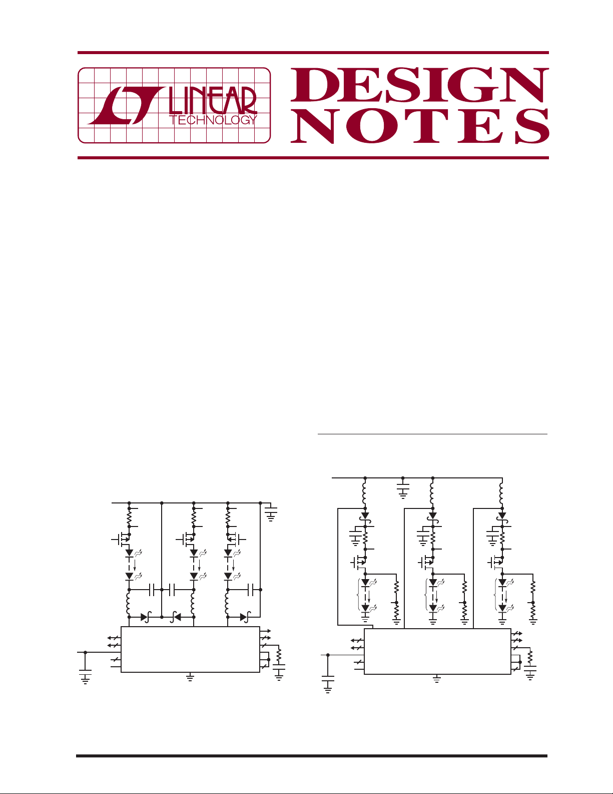
Figure 1. Triple Buck Mode Can Drive 3x 500mA LED Strings
09/08/449
V
IN
3.3V OR 5V
PWM1- 3
C5
1μF
6.3V
SW1 SW2
CAP1-3
LED1-3
V
IN
PWM1- 3
SHDN
SHDN
C1: TAIYO YUDEN UMK325BJ105MH
C2-C4: MURATA GRM21BR71H105K
D1-D3: ROHM RB160M-60
LT3496
GND
SW3 TG1-3
OVP1-3
VC1-3
V
REF
FADJ
CTRL1-3
L1-L3: SUMIDA CDRH3D14/HP-150
M1-M3: ZETEX ZXMP6A13F
DN449 F02
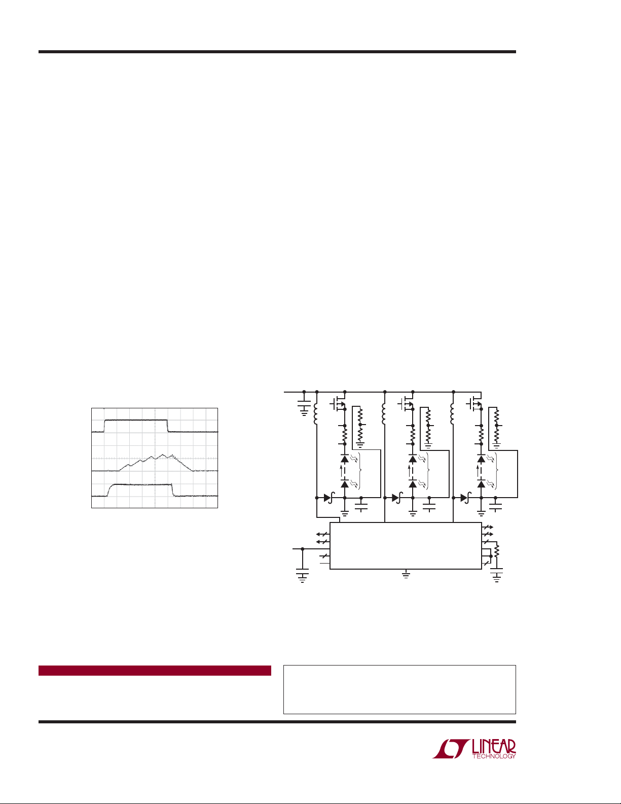
Figure 2. Triple Boost Mode Can Drive 200mA LEDs
18.2k
1nF
Buck Mode Circuit Drives Three 500mA LED Strings
Figure 1 shows a triple buck mode LED driver. Each channel drives 500mA of current to its LEDs. Each string can
have from eight to twelve LEDs, depending on type. The
2.1MHz switching frequency minimizes the solution size
by allowing the use of low profi le inductors and capacitors. The overall size of the circuit is less than 16mm ×
16mm, with a maximum height of 1.5mm.
Effi ciency can be above 95% for a LT3496 buck mode
driver. A further reduction in the parts count is possible
by removing M1, M2 and M3. However, the dimming ratio
drops without those MOSFETs. To improve the effi ciency,
pin should be biased from a 3.3V or 5V supply.
the V
IN
Energy to the LEDs is supplied by PV
. OVP protection
IN
is omitted in Figure 1.
Boost Mode Circuit Drives Three 200mA LED Strings
Figure 2 shows a triple boost mode driver that delivers
200mA to each LED string from a regulated 12V. Figure 3
shows the superior PWM dimming performance of the
circuit. The LED current reaches a programmed 200mA
in less than 500ns. The effi ciency of this circuit is 90%
at a 2.1MHz switching frequency. Unlike the buck mode
driver, the boost mode and buck-boost mode drivers
always require an OVP circuit at the output for open LED
protection.
PWM
5V/DIV
(100Hz)
Buck-Boost Mode Circuit Survives Load Dump Events
In automotive applications, load dump is a condition under which an IC is expected to experience 40V transient.
In such applications, the LED string voltage often falls
in the middle of the 8V to 40V input supply range, thus
requiring buck-boost mode.
In a buck-boost circuit, the switch voltage is the sum of
the input voltage and the LED voltage. Therefore, it is
necessary to turn off the internal power switch before
the input voltage gets too high. The LT3496 circuit in
Figure 4 drives four LEDs, at 200mA per channel. The
circuit monitors the Schottky diodes’ cathode voltage
). The OVP logic turns off the main switch when VSC
(V
SC
is above 38V, preventing the switch voltage from rising
further. Since no IC pin experiences absolute maximum
voltage, the circuit survives the load dump event.
Conclusion
Multiple output LED drivers, such as the LT3496, offer
excellent current matching, effi ciency and space savings. The fl exibility to operate in buck, boost or buckboost mode makes the LT3496 feasible in many rugged
applications.
PVIN, 8V TO 16V
40V TRANSIENT
50V
C1
1μF
L1
15μH
LED1
CAP1
0.5Ω
M1
7.15M
OVP1
191k
TG2TG1
L2
15μH
LED2
CAP2
0.5Ω
M2
7.15M
OVP2
191k
TG3
L3
15μH
LED3
CAP3
0.5Ω
M3
7.15M
OVP3
191k
I
L
500mA/DIV
I
LED
200mA/DIV
0.5μs/DIV
DN449 F03
Figure 3. Achieving Greater Than 3000:1 PWM
Dimming Ratio with a PMOS Disconnect
Data Sheet Download
www.linear.com
Linear Technology Corporation
1630 McCarthy Blvd., Milpitas, CA 95035-7417
(408) 432-1900
●
FAX: (408) 434-0507 ● www.linear.com
200mA
D1 D2 D3
V
SW1 SW2
3.3V OR 5V
C8
1μF
6.3V
V
IN
CAP1-3
LED1-3
V
IN
PWM
PWM1- 3
SHDN
SHDN
C1: TAIYO YUDEN UMK325BJ105MH
C3, C5, C7: TAIYO YUDEN TMK212BJ225MG
D1-D3: ROHM RB160M-60TR
4 LEDs
200mA
SC
C3
2.2μF
25V
PV
IN
LT3496
GND
4 LEDs
200mA
V
SC
C5
2.2μF
25V
PV
IN
SW3 TG1-3
L1-L3: SUMIDA CDRH3D14/HP-150
M1-M3: ZETEX ZXMP6A13F
OVP1-3
VC1-3
V
FADJ
CTRL1-3
V
REF
DN449 F04
4 LEDs
SC
C7
2.2μF
25V
PV
IN
18.2Ω
1nF
Figure 4. Triple Buck-Boost Mode Can Drive
200mA LEDs While Surviving Load Dump
For applications help,
call (408) 432-1900, Ext. 2759
dn449 LT/TP 0908 246K • PRINTED IN THE USA
© LINEAR TECHNOLOGY CORPORATION 2008
 Loading...