

LT3494/LT3494A
Micropower Low Noise
Boost Converters with
Output Disconnect
FEATURES
■
Low Quiescent Current
65μA in Active Mode
1μA in Shutdown Mode
■
Switching Frequency is Non-Audible Over Entire
Load Range
■
Integrated Power NPN:
350mA Current Limit (LT3494A)
180mA Current Limit (LT3494)
■
Integrated Schottky Diode
■
Integrated Output Disconnect
■
Integrated Output Dimming
■
Wide Input Range: 2.3V to 16V
■
Wide Output Range: Up to 40V
■
Tiny 8-Lead 3mm × 2mm DFN Package
APPLICATIONS
■
OLED Power
■
Low Noise Power
■
MP3 Players
DESCRIPTION
The LT®3494/LT3494A are low noise boost converters
with integrated power switch, Schottky diode and output
disconnect circuitry. The parts use a novel* control technique resulting in low output voltage ripple as well as high
effi ciency over a wide load current range. This technique
guarantees that the switching frequency stays above the
audio band for the entire load range. The parts feature a high
performance NPN power switch with a 350mA and 180mA
current limit for the LT3494A and LT3494 respectively. The
quiescent current is a low 65μA, which is further reduced
to less than 1μA in shutdown. The internal disconnect
circuitry allows the output voltage to be isolated from the
input during shutdown. An auxiliary reference input (CTRL
pin) overrides the internal 1.225V feedback reference with
any lower value allowing full control of the output voltage
during operation. The LT3494/LT3494A are available in a
tiny 8-lead 3mm × 2mm DFN package.
, LT, LTC and LTM are registered trademarks of Linear Technology Corporation.
All other trademarks are the property of their respective owners.
*Patent pending.
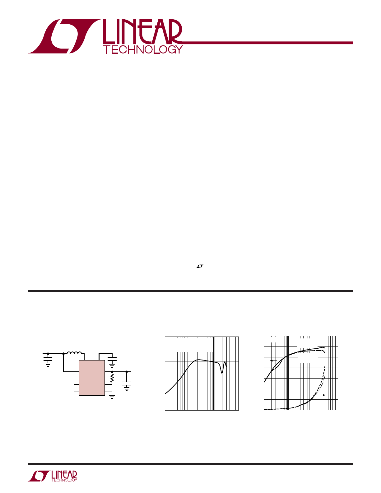
TYPICAL APPLICATION
OLED Power Supply from One Li-Ion Cell
4.7μF
15μH
SW CAP
V
V
CC
LT3494
SHDN
CTRL
GND
0.22μF
OUT
2.21M
FB
3494 TA01a
V
TO 4.2V
IN
3V
V
OUT
16V
16mA
2.2μF
Output Voltage Ripple
vs Load Current
15
LT3494
FIGURE 5 CIRCUIT
100MHz MEASUREMENT BW
10
5
PEAK-TO-PEAK RIPPLE (mV)
OUT
V
0
0.1
1 10 100
LOAD CURRENT (mA)
3494 TA01b
Effi ciency and Power Loss
vs Load Current
90
VIN = 3.6V
80
70
60
50
EFFICIENCY (%)
40
30
20
0.1
LOAD FROM
CAPACITOR
LOAD FROM
1 10 100
LOAD CURRENT (mA)
280
240
POWER LOSS (mW)
V
OUT
200
160
120
80
40
0
3494 TA01c
3494fb
1
LT3494/LT3494A
(Note 1)
VCC Voltage ...............................................................16V
SW Voltage ...............................................................40V
CAP Voltage ..............................................................40V
Voltage .............................................................40V
V
OUT
SHDN Voltage ...........................................................16V
CTRL Voltage ............................................................16V
FB Voltage ................................................................2.5V
Maximum Junction Temperature .......................... 125°C
Operating Temperature Range (Note 2) ... –40°C to 85°C
Storage Temperature Range ................... –65°C to 125°C
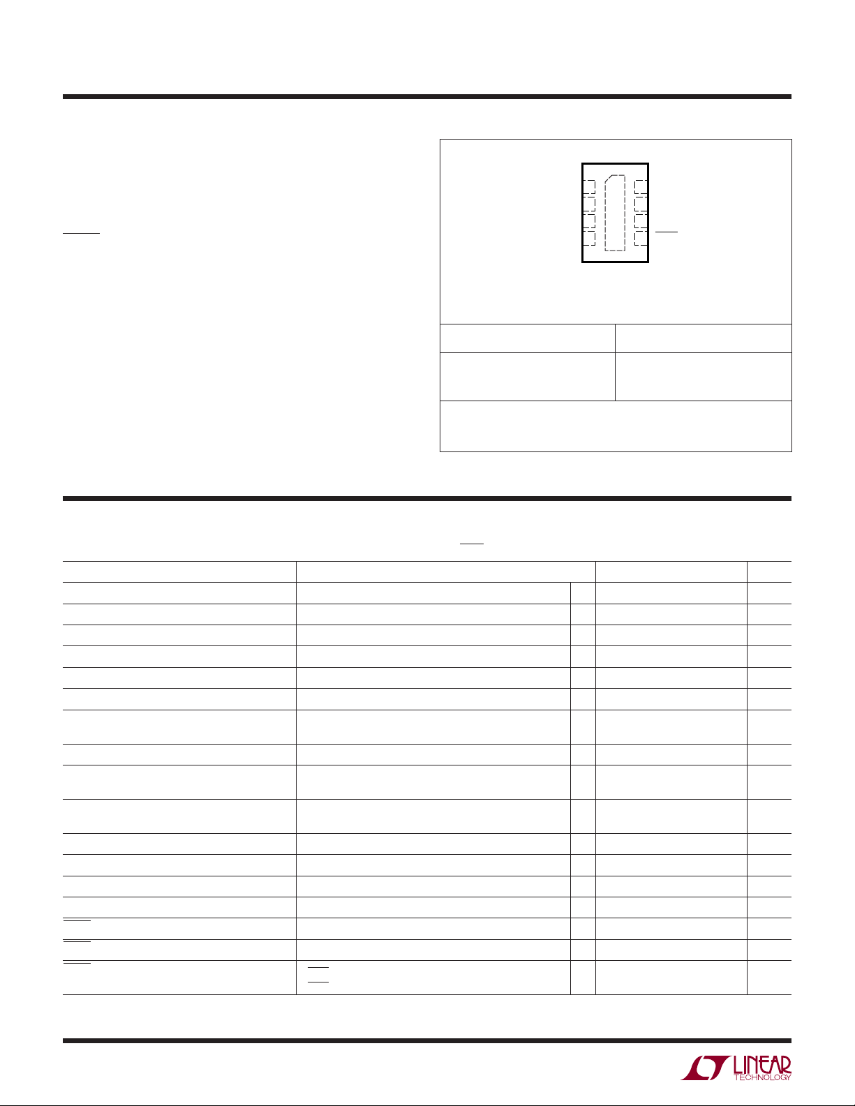
PACKAGE/ORDER INFORMATIONABSOLUTE MAXIMUM RATINGS
TOP VIEW
CAP
1SW
GND
2
V
3
CC
CTRL
4
8-LEAD (3mm × 2mm) PLASTIC DFN
EXPOSED PAD (PIN 9) IS GND, MUST BE SOLDERED TO PCB
DDB PACKAGE
T
= 125°C, θJA = 76°C/W
JMAX
ORDER PART NUMBER DDB PART MARKING
8
V
7
9
OUT
FB
6
SHDN
5
LT3494EDDB
LT3494AEDDB
Order Options Tape and Reel: Add #TR
Lead Free: Add #PBF Lead Free Tape and Reel: Add #TRPBF
Lead Free Part Marking: http://www.linear.com/leadfree/
Consult LTC Marketing for parts specifi ed with wider operating temperature ranges.
ELECTRICAL CHARACTERISTICS
The
temperature range, otherwise specifi cations are at T
PARAMETER CONDITIONS MIN TYP MAX UNITS
Minimum Operating Voltage 2.3 2.5 V
Maximum Operating Voltage 16 V
Feedback Voltage V
FB Resistor
Quiescent Current Not Switching 65 75 μA
Quiescent Current in Shutdown V
Minimum Switch Off Time After Start-Up Mode, V
Maximum Switch Off Time V
Switch Current Limit LT3494A (Note 5)
Switch V
CESAT
Switch Leakage Current V
Schottky Forward Voltage I
Schottky Reverse Leakage 0.05 1 μA
PMOS Disconnect V
SHDN Input Voltage High 1.5 V
SHDN Input Voltage Low 0.3 V
SHDN Pin Bias Current V
CAP
– V
OUT
CTRL
⎯S⎯H⎯D⎯
During Start-Up Mode, V
FB
LT3494 (Note 5)
LT3494A, ISW = 200mA
LT3494, I
SW
DIODE
I
OUT
SHDN
V
SHDN
= 25°C. VCC = 3V, V
A
= 3V (Note 3)
= 0V, VCC = 3V 0 1 μA
N
= 1.5V
= 100mA
SW
= 5V, V
⎯S⎯H⎯D⎯
= 100mA 900 1100 mV
= 10mA, V
= 3V
= 0V
●
denotes the specifi cations which apply over the full operating
= VCC, unless otherwise noted. (Note 2)
SHDN
●
1.205 1.225 1.245 V
●
179 182 184 kΩ
= 1V, V
FB
= 0.2V, V
FB
= 0 0.01 1 μA
N
= 5V 250 mV
CAP
= 3V (Note 4)
CTRL
CTRL
= 3V (Note 4)
●
15 20 30 μs
225
115
100
450
350
180
180
110
5
0
LCCD
LCRW
450
250
10
0.1
mA
mA
mV
mV
μA
μA
ns
ns
2
3494fb
LT3494/LT3494A
ELECTRICAL CHARACTERISTICS
The
temperature range, otherwise specifi cations are at T
PARAMETER CONDITIONS MIN TYP MAX UNITS
CTRL Pin Bias Current V
CTRL to FB Offset V
Maximum Shunt Current V
CTRL
CTRL
FB
= 25°C. VCC = 3V, V
A
= 0.5V, Current Flows Out of Pin
= 0.5V 8 15 mV
= 1.3V, V
CAP
●
denotes the specifi cations which apply over the full operating
= VCC, unless otherwise noted. (Note 2)
SHDN
●
20 100 nA
= 5V 230 μA
Note 1: Stresses beyond those listed under Absolute Maximum Ratings
may cause permanent damage to the device. Exposure to any Absolute
Maximum Rating condition for extended periods may affect device
reliability and lifetime.
Note 2: The LT3494/LT3494A are guaranteed to meet performance
specifi cations from 0°C to 85°C. Specifi cations over the –40°C to 85°C
operating temperature range are assured by design, characterization and
correlation with statistical process controls.
Note 3: Internal reference voltage is determined by fi nding V
level which causes quiescent current to increase 20μA above “Not
Switching” level.
Note 4: If CTRL is overriding the internal reference, Start-Up mode occurs
when V
is less then half the voltage on CTRL. If CTRL is not overriding
FB
the internal reference, Start-Up mode occurs when V
voltage of the internal reference.
Note 5: Current limit guaranteed by design and/or correlation to static test.
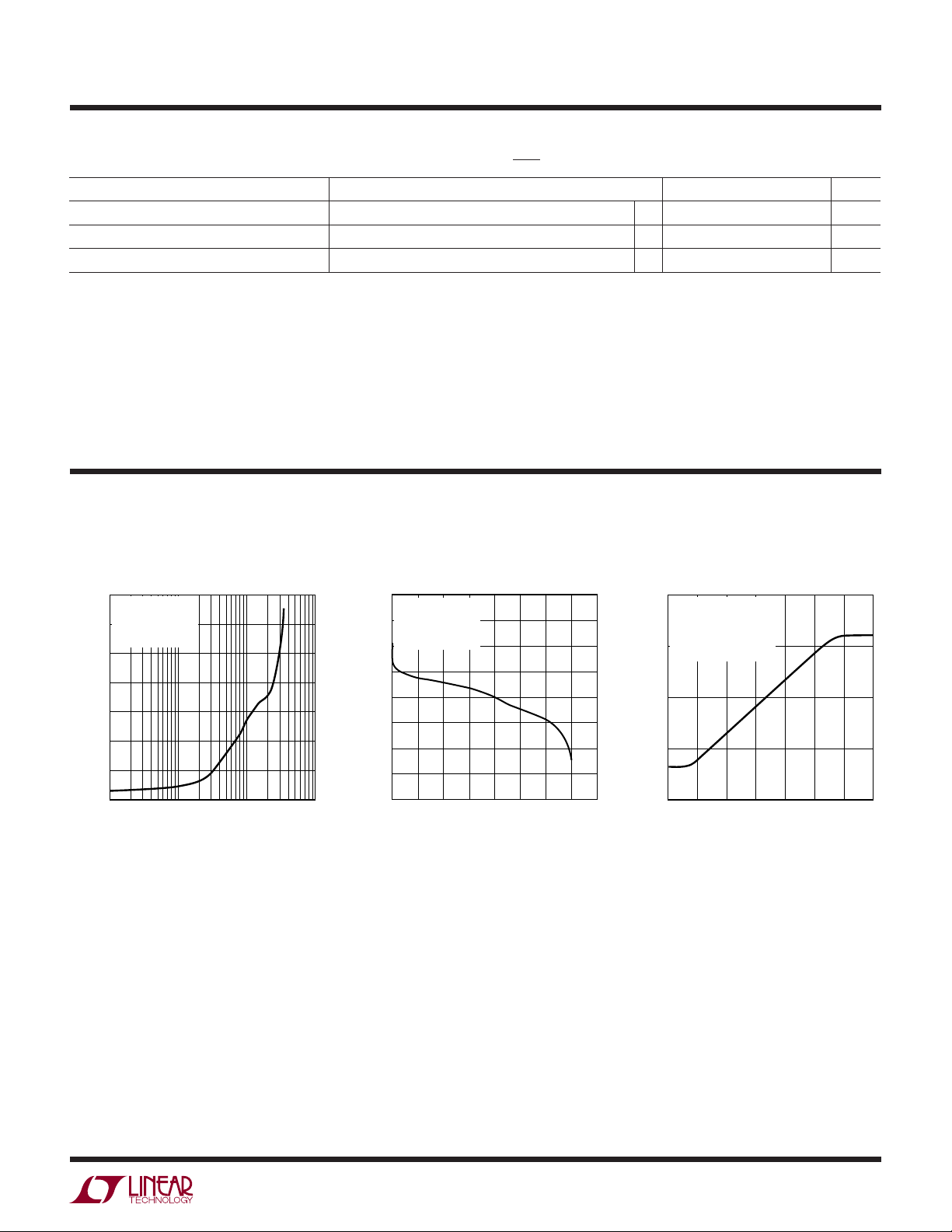
TYPICAL PERFORMANCE CHARACTERISTICS
Switching Frequency
vs Load Currrent
1400
LT3494
FIGURE 5 CIRCUIT
1200
1000
SWITCHING FREQUENCY (kHz)
800
600
400
200
= 3.6V
V
CC
= 16V
V
OUT
0
0.1
1 10 100
LOAD CURRENT (mA)
3494 G01
Load Regulation V
2.0
LT3494
FIGURE 5 CIRCUIT
1.5
= 3.6V
V
CC
= 16V
V
OUT
1.0
0.5
0
–0.5
VOLTAGE CHANGE (%)
OUT
–1.0
V
–1.5
–2.0
5
0
10
20
15
LOAD CURRENT (mA)
25
30
TA = 25°C unless otherwise noted.
vs CTRL Voltage
OUT
20
LT3494
FIGURE 5 CIRCUIT
= 3.6V
V
CC
= 16V
V
OUT
15
LOAD CURRENT = 1mA
10
VOLTAGE (V)
OUT
V
5
35
3494 G02
40
0
0.1
0.3 0.5 0.7 0.9
CTRL VOLTAGE (V)
voltage
FB
is less then half the
FB
1.1 1.3 1.5
3494 G03
3494fb
3
LT3494/LT3494A
TYPICAL PERFORMANCE CHARACTERISTICS
Output Voltage vs Temperature Minimum Switching Frequency
2.0
LT3494
FIGURE 5 CIRCUIT
1.5
1.0
0.5
0
–0.5
–1.0
OUTPUT VOLTAGE CHANGE (%)
–1.5
–2.0
–40
–20
0
40
20
TEMPERATURE (°C)
60
100
3494 G04
120
80
SHDN Current vs SHDN Voltage Peak Inductor Current (LT3494)
20
15
51.0
VCC = 3.6V
NO LOAD
50.5
50.0
49.5
49.0
48.5
48.0
SWITCHING FREQUENCY (kHz)
47.5
47.0
–20
–40
400
350
300
0
TEMPERATURE (°C)
FIGURE 5 CIRCUIT
= 3.6V
V
CC
= 16V
V
OUT
20
40
60
TA = 25°C unless otherwise noted.
Quiescent Current–Not Switching
100
95
90
85
80
(μA)
75
VCC
I
70
65
60
55
50
3
100
3494 G05
120
80
4
Peak Inductor Current (LT3494A)
700
FIGURE 6 CIRCUIT
= 3.6V
V
CC
650
600
= 16V
V
OUT
5
V
CC
8
(V)
7
6
9
10
3494 G06
10
5
SHDN PIN CURRENT (μA)
0
V
OUT
10mV/DIV
COUPLED
SW
VOLTAGE
10V/DIV
INDUCTOR
CURRENT
50mA/DIV
0
2468
SHDN PIN VOLTAGE (V)
10 12 14 16
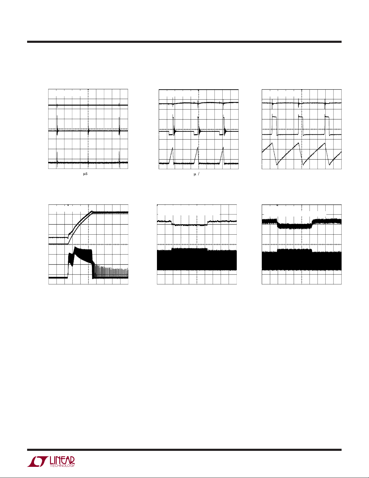
LT3494 Switching Waveforms at
No Load
FIGURE 5 CIRCUIT
AC
= 3.6V
V
CC
= 16V
V
OUT
5μs/DIV
3494 G07
3494 G10
250
200
150
PEAK INDUCTOR CURRENT (mA)
100
–40
040
–20 20
TEMPERATURE (°C)
LT3494 Switching Waveforms at
1mA Load
FIGURE 5 CIRCUIT
V
OUT
10mV/DIV
AC
COUPLED
SW
VOLTAGE
10V/DIV
INDUCTOR
CURRENT
100mA/DIV
= 3.6V
V
CC
= 16V
V
OUT
2μs/DIV
550
500
450
PEAK INDUCTOR CURRENT (mA)
400
80
60
100
120
3494 G08
–40
040
–20 20
TEMPERATURE (°C)
80
60
100
120
3494 G09
LT3494 Switching Waveforms at
25mA Load
FIGURE 5 CIRCUIT
V
OUT
10mV/DIV
AC
COUPLED
SW
VOLTAGE
10V/DIV
INDUCTOR
CURRENT
100mA/DIV
3494 G11
V
V
CC
OUT
= 3.6V
= 16V
500ns/DIV
3494 G12
4
3494fb
LT3494/LT3494A
TYPICAL PERFORMANCE CHARACTERISTICS
V
OUT
10mV/DIV
AC
COUPLED
SW
VOLTAGE
10V/DIV
INDUCTOR
CURRENT
50mA/DIV
CAP
VOLTAGE
5V/DIV
V
OUT
VOLTAGE
5V/DIV
INDUCTOR
CURRENT
100mA/DIV
LT3494A Switching Waveforms at
No Load
FIGURE 6 CIRCUIT
10mV/DIV
COUPLED
VOLTAGE
INDUCTOR
CURRENT
V
V
CC
OUT
= 3.6V
= 16V
5ms/DIV
3494 G13
100mA/DIV
LT3494 Start-Up Waveforms LT3494 Transient Response LT3494A Transient Response
FIGURE 5 CIRCUIT
VOLTAGE
50mV/DIV
AC COUPLED
INDUCTOR
CURRENT
100mA/DIV
LT3494A Switching Waveforms at
5mA Load
FIGURE 6 CIRCUIT
V
OUT
AC
SW
10V/DIV
= 3.6V
CC
= 16V
V
OUT
FIGURE 5 CIRCUIT
10mA→15mA→10mA LOAD PULSE
V
OUT
2ms/DIVV
TA = 25°C unless otherwise noted.
LT3494A Switching Waveforms at
30mA Load
FIGURE 6 CIRCUIT
V
OUT
10mV/DIV
AC
COUPLED
SW
VOLTAGE
10V/DIV
INDUCTOR
CURRENT
200mA/DIV
3494 G14
50mV/DIV
COUPLED
INDUCTOR
CURRENT
200mA/DIV
= 3.6V
CC
= 16V
V
OUT
FIGURE 6 CIRCUIT
15mA→30mA→15mA LOAD PULSE
V
OUT
AC
500ns/DIVV
3494 G15
V
V
CC
OUT
= 3.6V
= 16V
200μs/DIV
3494 G16
V
V
CC
OUT
= 3.6V
= 16V
100μs/DIV
3494 G17
V
CC
OUT
= 3.6V
= 16V
100μs/DIVV
3494 G18
3494fb
5

LT3494/LT3494A
PIN FUNCTIONS
SW (Pin 1): Switch Pin. This is the collector of the internal
NPN power switch. Minimize the metal trace area connected
to this pin to minimize EMI.
GND (Pin 2): Ground. Tie directly to local ground plane.
(Pin 3): Input Supply Pin. Must be locally
V
CC
bypassed.
CTRL (Pin 4): Dimming Pin. If not used, tie CTRL to 1.5V
or higher. If in use, drive CTRL below 1.225V to override
the internal reference. See Applications Information for
more information.
SHDN (Pin 5): Shutdown Pin. Tie to 1.5V or more to
enable device. Ground to shut down.
BLOCK DIAGRAM
FB (Pin 6): Feedback Pin. Reference voltage is 1.225V.
There is an internal 182k resistor from the FB pin to GND.
To achieve the desired output voltage, choose R1 according to the following formula:
V
⎛
OUT MAX
R
1 182
•
V
(Pin 7): Drain of Output Disconnect PMOS. Place a
OUT
⎜
⎝
()
1 225
.
⎞
k
1=
–
Ω
⎟
⎠
bypass capacitor from this pin to GND. See Applications
Information.
CAP (Pin 8): This is the cathode of the internal Schottky
diode. Place a bypass capacitor from this pin to GND.
Exposed Pad (Pin 9): Ground. This pin must be soldered
to PCB.
).054
6
##
34!2450#/.42/,
&"
K
#42,
3($.
n
6
2%&
37)4#(#/.42/,
37
'.$
#!0
$)3#/..%#4
#/.42/,
3(5.4#/.42/,
6
/54
2
"$
/54054
6
3494fb
OPERATION
LT3494/LT3494A
The LT3494/LT3494A use a novel control scheme to provide high effi ciency over a wide range of output current.
In addition, this technique keeps the switching frequency
above the audio band over all load conditions.
The operation of the part can be better understood by
refering to the Block Diagram. The part senses the output
voltage by monitoring the voltage on the FB pin. The user
sets the desired output voltage by choosing the value of
the external top feedback resistor. The parts incorporate
a precision 182k bottom feedback resistor. Assuming that
output voltage adjustment is not used (CTRL pin is tied to
1.5V or greater), the internal reference (V
= 1.225V) sets
REF
the voltage at which FB will servo to during regulation.
The Switch Control block senses the output of the amplifi er and adjusts the switching frequency as well as other
parameters to achieve regulation. During the start-up of
the circuit, special precautions are taken to insure that the
inductor current remains under control.
Because the switching frequency is never allowed to fall
below approximately 50kHz, a minimum load must be
present to prevent the output voltage from drifting too high.
This minimum load is automatically generated within the
part via the Shunt Control block. The level of this current
is adaptable, removing itself when not needed to improve
effi ciency at higher load levels.
The LT3494/LT3494A also have an integrated Schottky
diode and PMOS output disconnect switch. The PMOS
switch is turned on when the part is enabled via the SHDN
pin. When the parts are in shutdown, the PMOS switch
turns off, allowing the V
node to go to ground. This
OUT
type of disconnect function is often required in power
supplies.
The only difference between the LT3494A and LT3494
is the level of the current limit. The LT3494A has a typical peak current limit of 350mA while the LT3494 has a
180mA limit.
APPLICATIONS INFORMATION
Choosing an Inductor
Several recommended inductors that work well with the
LT3494/LT3494A are listed in Table 1, although there are
many other manufacturers and devices that can be used.
Consult each manufacturer for more detailed information
and for their entire selection of related parts. Many different sizes and shapes are available. Use the equations
and recommendations in the next few sections to fi nd the
correct inductance value for your design.
Inductor Selection—Boost Regulator
The formula below calculates the appropriate inductor
value to be used for a boost regulator using the LT3494/
LT3494A (or at least provides a good starting point).
Table 1. Recommended Inductors
PART FOR USE WITH
LQH32CN100K53
LQH32CN150K53
CDRH3D11-100
CDHED13/S-150
LT3494/LT3494A
LT3494
LT3494
LT3494/LT3494A
VALUE
(μH)
10
15
10
15
MAX DCR
(Ω)
0.3
0.58
0.24
0.55
This value provides a good trade off in inductor size and
system performance. Pick a standard inductor close to
this value. A larger value can be used to slightly increase
the available output current, but limit it to around twice
the value calculated below, as too large of an inductance
will decrease the output voltage ripple without providing
much additional output current. A smaller value can be
used (especially for systems with output voltages greater
than 12V) to give a smaller physical size. Inductance can
be calculated as:
L = (V
where V
– V
OUT
is the desired output voltage and V
OUT
+ 0.5V) • 0.66 (μH)
IN(MIN)
IN(MIN)
is
the minimum input voltage. Generally, a 10μH or 15μH
inductor is a good choice.
MAX DC I
(mA)
450
300
280
550
SIZE
(mm × mm × mm) VENDOR
3.5 × 2.7 × 1.7
3.5 × 2.7 × 1.7
4.0 × 4.0 × 1.2
4.0 × 4.2 × 1.4
Murata
www.murata.com
Sumida
www.sumida.com
3494fb
7
LT3494/LT3494A
APPLICATIONS INFORMATION
Capacitor Selection
The small size and low ESR of ceramic capacitors makes
them suitable for most LT3494/LT3494A applications. X5R
and X7R types are recommended because they retain their
capacitance over wider voltage and temperature ranges
than other types such as Y5V or Z5U. A 4.7μF input capacitor and a 2.2μF to 10μF output capacitor are suffi cient for
most LT3494/LT3494A applications. Always use a capacitor
with a suffi cient voltage rating. Many capacitors rated at
2.2μF to 10μF, particularly 0805 or 0603 case sizes, have
greatly reduced capacitance when bias voltages are applied. Be sure to check actual capacitance at the desired
output voltage. Generally a 1206 size capacitor will be
adequate. A 0.22μF or 0.47μF capacitor placed on the
CAP node is recommended to fi lter the inductor current
while the larger 2.2μF to 10μF placed on the V
OUT
node
will give excellent transient response and stability. Table 2
shows a list of several capacitor manufacturers. Consult
the manufacturers for more detailed information and for
their entire selection of related parts.
Table 2. Recommended Ceramic Capacitor Manufacturers
MANUFACTURER PHONE URL
Taiyo Yuden 408-573-4150 www.t-yuden.com
AVX 843-448-9411 www.avxcorp.com
Murata 814-237-1431 www.murata.com
Kemet 408-986-0424 www.kemet.com
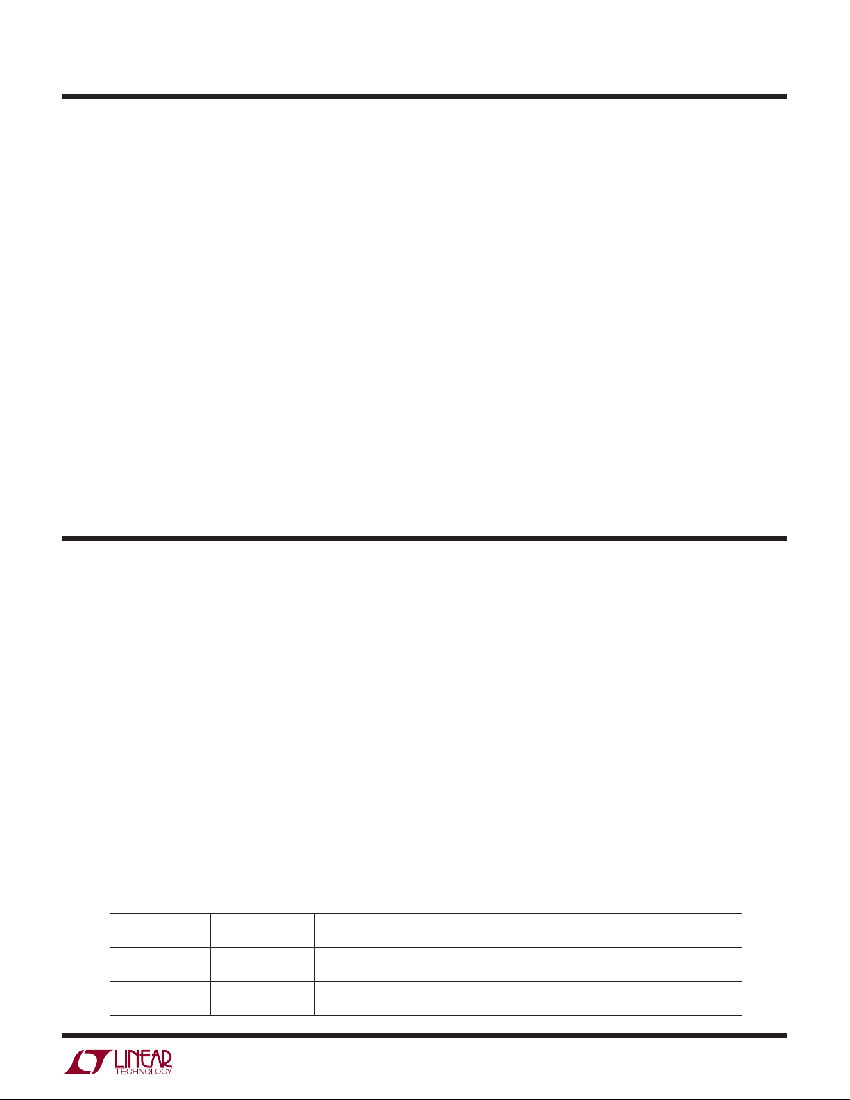
1.500
1.250
1.000
0.750
FB VOLTAGE (V)
0.500
0.250
0
0
0.5 .75 1.0
.25
CTRL VOLTAGE (V)
1.25 1.5
3494 F01
Figure 1. CTRL to FB Transfer Curve
To set the maximum output voltage, select the values of
R1 according to the following equation:
V
R
1 182
⎛
•
⎜
⎝
OUT MAX
()
1 225
.
⎞
k
1=
–
Ω
⎟
⎠
When CTRL is used to override the internal reference,
the output voltage can be lowered from the maximum
value down to nearly the input voltage level. If the voltage
source driving the CTRL pin is located at a distance to the
LT3494/LT3494A, a small 0.1μF capacitor may be needed
to bypass the pin locally.
Choosing a Feedback Node
Setting Output Voltage and
the Auxiliary Reference Input
The LT3494/LT3494A are equipped with both an internal
1.225V reference and an auxiliary reference input. This allows the user to select between using the built-in reference
and supplying an external reference voltage. The voltage
at the CTRL pin can be adjusted while the chip is operating to alter the output voltage of the LT3494/LT3494A for
purposes such as display dimming or contrast adjustment.
To use the internal 1.225V reference, the CTRL pin must be
held higher than 1.5V. When the CTRL pin is held between
0V and 1.5V, the LT3494 will regulate the output such that
the FB pin voltage is nearly equal to the CTRL pin voltage.
At CTRL voltages close to 1.225V, a soft transition occurs
between the CTRL pin and the internal reference. Figure 1
shows this behavior.
8
The single feedback resistor may be connected to the V
pin or to the CAP pin (see Figure 2). Regulating the V
OUT
OUT
pin eliminates the output offset resulting from the voltage
drop across the output disconnect PMOS. Regulating the
CAP pin does not compensate for the voltage drop across
the output disconnect, resulting in an output voltage V
OUT
that is slightly lower than the voltage set by the resistor
divider. Under most conditions, it is advised that the
feedback resistor be tied to the V
18
SW CAP
3
5
4
V
CC
SHDN
CTRL
LT3494
V
GND
OUT
FB
Figure 2. Feedback Connection Using the CAP Pin or the V
C1
7
R1
6
2
V
OUT
C3
pin.
OUT
18
SW CAP
3
V
CC
LT3494
5
SHDN
4
CTRL
V
GND
OUT
C1
7
R1
6
FB
2
3494 F02
Pin
OUT
3494fb

APPLICATIONS INFORMATION
LT3494/LT3494A
Connecting the Load to the CAP Node
The effi ciency of the converter can be improved by connecting the load to the CAP pin instead of the V
OUT
pin.
The power loss in the PMOS disconnect circuit is then
made negligible. By connecting the feedback resistor to
the V
pin, no quiescent current will be consumed in the
OUT
feedback resistor string during shutdown since the PMOS
transistor will be open (see Figure 3). The disadvantage
of this method is that the CAP node cannot go to ground
during shutdown, but will be limited to around a diode
drop below V
. Loads connected to the part should only
CC
sink current. Never force external power supplies onto
the CAP or V
pins. The larger value output capacitor
OUT
(2.2μF to 10μF) should be placed on the node to which
the load is connected.
18
SW CAP
3
V
CC
LT3494
5
SHDN
4
CTRL
Figure 3. Improved Effi ciency
V
GND
OUT
7
6
FB
2
3494 F03
I
C1
LOAD
If the inductor ripple current is greater than the peak current, then the circuit will only operate in discontinuous
conduction mode. The inductor value should be increased
so that I
< IPK. An application circuit can be designed
RIPPLE
to operate only in discontinuous mode, but the output
current capability will be reduced.
Step 3: Calculate the average input current:
IIIamps
IN AVG PK
()
–=
RIPPLE
2
Step 4: Calculate the nominal output current:
••.
075
amps
OUT
I
OUT NOM
()
IV
IN AVG IN
()
=
V
Step 5: Derate output current:
I
OUT
= I
OUT(NOM)
• 0.7 amps
For low output voltages the output current capability will
be increased. When using output disconnect (load current taken from V
), these higher currents will cause
OUT
the drop in the PMOS switch to be higher resulting in
reduced output current capability than those predicted
by the preceding equations.
Maximum Output Load Current
The maximum output current of a particular LT3494/
LT3494A circuit is a function of several circuit variables.
The following method can be helpful in predicting the
maximum load current for a given circuit:
Step 1: Calculate the peak inductor current:
–
9
amps
II
PK LIMIT
where I
V
••
400 10
=+
IN
L
is 0.180A and 0.350A for the LT3494 and
LIMIT
LT3494A respectively. L is the inductance value in Henrys
and V
is the input voltage to the boost circuit.
IN
Step 2: Calculate the inductor ripple current:
9
–
amps
I
RIPPLE
where V
1 150 10
VV
()
OUT IN
=
–••
+
L
is the desired output voltage.
OUT
Inrush Current
When V
is stepped from ground to the operating volt-
CC
age while the output capacitor is discharged, a higher
level of inrush current may fl ow through the inductor
and integrated Schottky diode into the output capacitor.
Conditions that increase inrush current include a larger
more abrupt voltage step at V
, a larger output capacitor
IN
tied to the CAP pin and an inductor with a low saturation
current. While the internal diode is designed to handle
such events, the inrush current should not be allowed to
exceed 1A. For circuits that use output capacitor values
within the recommended range and have input voltages
of less than 5V, inrush current remains low, posing no
hazard to the device. In cases where there are large steps
(more than 5V) and/or a large capacitor is used
at V
CC
at the CAP pin, inrush current should be measured to
ensure safe operation. The LT3494A circuits experience
higher levels of current during start-up and steady-state
operation. An external diode placed from the SW pin to
3494fb
9
LT3494/LT3494A
APPLICATIONS INFORMATION
the CAP pin will improve effi ciency and lower the stress
placed on the internal Schottky diode.
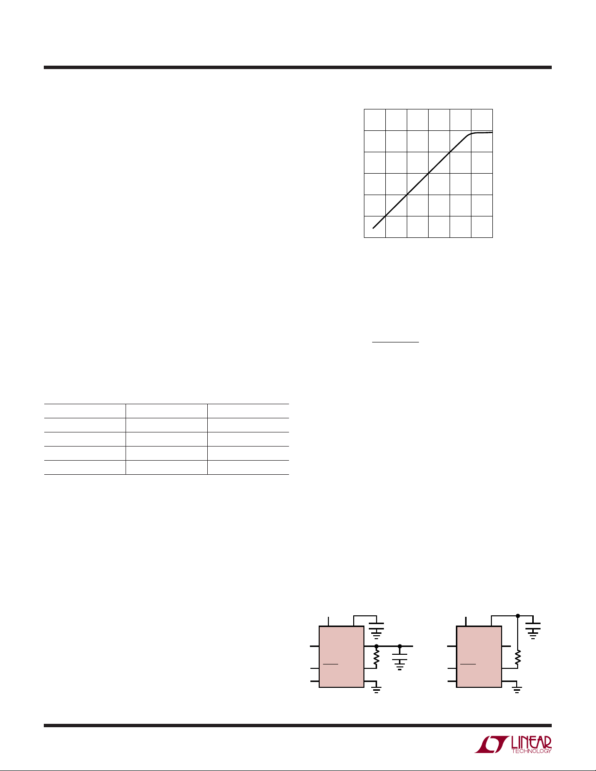
Board Layout Considerations
As with all switching regulators, careful attention must be
paid to the PCB board layout and component placement.
To maximize effi ciency, switch rise and fall times are made
as short as possible. To prevent electromagnetic interference (EMI) problems, proper layout of the high frequency
switching path is essential. The voltage signal of the SW pin
has sharp rising and falling edges. Minimize the length and
area of all traces connected to the SW pin and always use
a ground plane under the switching regulator to minimize
interplane coupling. In addition, the FB connection for
the feedback resistor R1 should be tied directly from the
Vout pin to the FB pin and be kept as short as possible,
ensuring a clean, noise-free connection. Recommended
component placement is shown in Figure 4.
TYPICAL APPLICATIONS
GND
SW
GND
V
CC
CTRL
CTRL
VIAS TO GROUND PLANE REQUIRED
TO IMPROVE THERMAL PERFORMANCE
GND
CAP
V
OUT
SHDN
FB
SHDN
Figure 4. Recommended Layout
3494 F04
L1
V
3V TO 4.2V
IN
C2
4.7μF
TURN ON/OFF
V
DIMMING
OUT
C1, C2: X5R OR X7R WITH SUFFICIENT VOLTAGE RATING
C3: MURATA GRM31MR71E225K
L1: MURATA LQH32CN150K53
15μH
SW CAP
3
V
CC
5
SHDN
4
CTRL
LT3494
V
GND
OUT
81
FB
C1
0.22μF
7
R1
6
2
3494 F05
C3
2.2μF
V
OUT
Figure 5. One Li-Ion Cell Input Boost Converter with the LT3494
V
OUT
(MΩ)
25 3.57 8.6
24 3.40 9.3
23 3.24 10.0
22 3.09 10.6
21 2.94 11.3
20 2.80 12.1
19 2.67 12.9
18 2.49 13.6
17 2.37 14.8
16 2.21 16.0
15 2.05 17.2
R1 VALUE REQUIRED
MAXIMUM OUTPUT CURRENT AT
3V INPUT (mA)
90
VIN = 3.6V
80
70
60
50
EFFICIENCY (%)
40
30
20
0.1
3.6V to 16V Effi ciency
LOAD FROM
CAPACITOR
LOAD FROM
V
OUT
1 10 100
LOAD CURRENT (mA)
3494 TA01c
280
240
POWER LOSS (mW)
200
160
120
80
40
0
3494fb
10
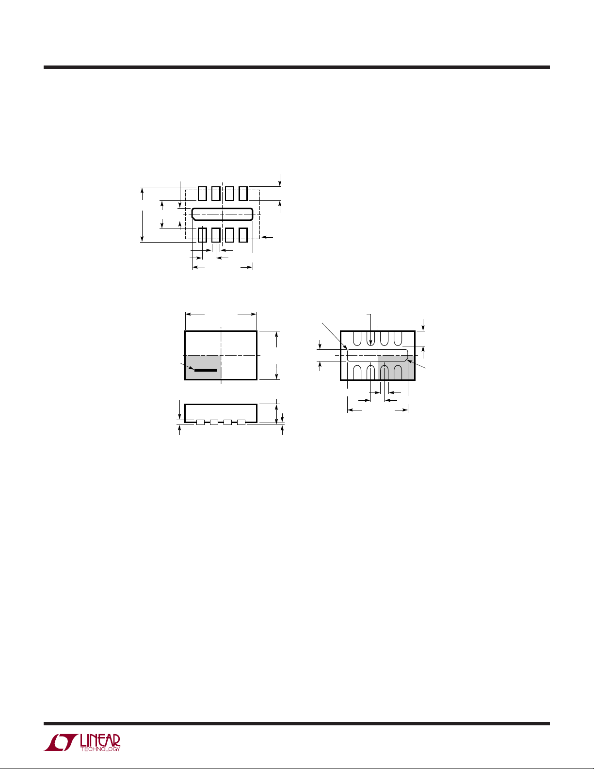
PACKAGE DESCRIPTION
0.61 ±0.05
(2 SIDES)
2.55 ±0.05
1.15 ±0.05
0.25 ± 0.05
RECOMMENDED SOLDER PAD PITCH AND DIMENSIONS
LT3494/LT3494A
DDB Package
8-Lead Plastic DFN (3mm × 2mm)
(Reference LTC DWG # 05-08-1702 Rev B)
0.70 ±0.05
PACKAGE
OUTLINE
0.50 BSC
2.20 ±0.05
(2 SIDES)
PIN 1 BAR
TOP MARK
(SEE NOTE 6)
0.200 REF
3.00 ±0.10
(2 SIDES)
2.00 ±0.10
(2 SIDES)
0.75 ±0.05
NOTE:
1. DRAWING CONFORMS TO VERSION (WECD-1) IN JEDEC PACKAGE OUTLINE M0-229
2. DRAWING NOT TO SCALE
3. ALL DIMENSIONS ARE IN MILLIMETERS
4. DIMENSIONS OF EXPOSED PAD ON BOTTOM OF PACKAGE DO NOT INCLUDE
MOLD FLASH. MOLD FLASH, IF PRESENT, SHALL NOT EXCEED 0.15mm ON ANY SIDE
5. EXPOSED PAD SHALL BE SOLDER PLATED
6. SHADED AREA IS ONLY A REFERENCE FOR PIN 1 LOCATION ON THE TOP AND BOTTOM OF PACKAGE
R = 0.05
0.56 ± 0.05
(2 SIDES)
0 – 0.05
R = 0.115
TYP
TYP
0.25 ± 0.05
2.15 ±0.05
(2 SIDES)
BOTTOM VIEW—EXPOSED PAD
0.40 ± 0.10
85
14
0.50 BSC
PIN 1
R = 0.20 OR
0.25 × 45°
CHAMFER
(DDB8) DFN 0905 REV B
Information furnished by Linear Technology Corporation is believed to be accurate and reliable.
However, no responsibility is assumed for its use. Linear Technology Corporation makes no representation that the interconnection of its circuits as described herein will not infringe on existing patent rights.
3494fb
11

LT3494/LT3494A
TYPICAL APPLICATION
L1
C2
4.7μF
10μH
V
IN
3V TO 4.2V
C1, C2: X5R OR X7R WITH SUFFICIENT VOLTAGE RATING
C3: TAIYO YUDEN TMK316BJ106ML
D1: CENTRAL SEMICONDUCTOR CMDSH-3
L1: MURATA LQH32CN100K53
SW CAP
3
V
CC
5
SHDN
4
CTRL
D1
V
LT3494A
OUT
GND
81
FB
C1
0.47μF
7
R1
6
2
3494 F06
C3
10μF
V
OUT
Figure 6. One Li-Ion Cell Input Boost Converter with the LT3494A
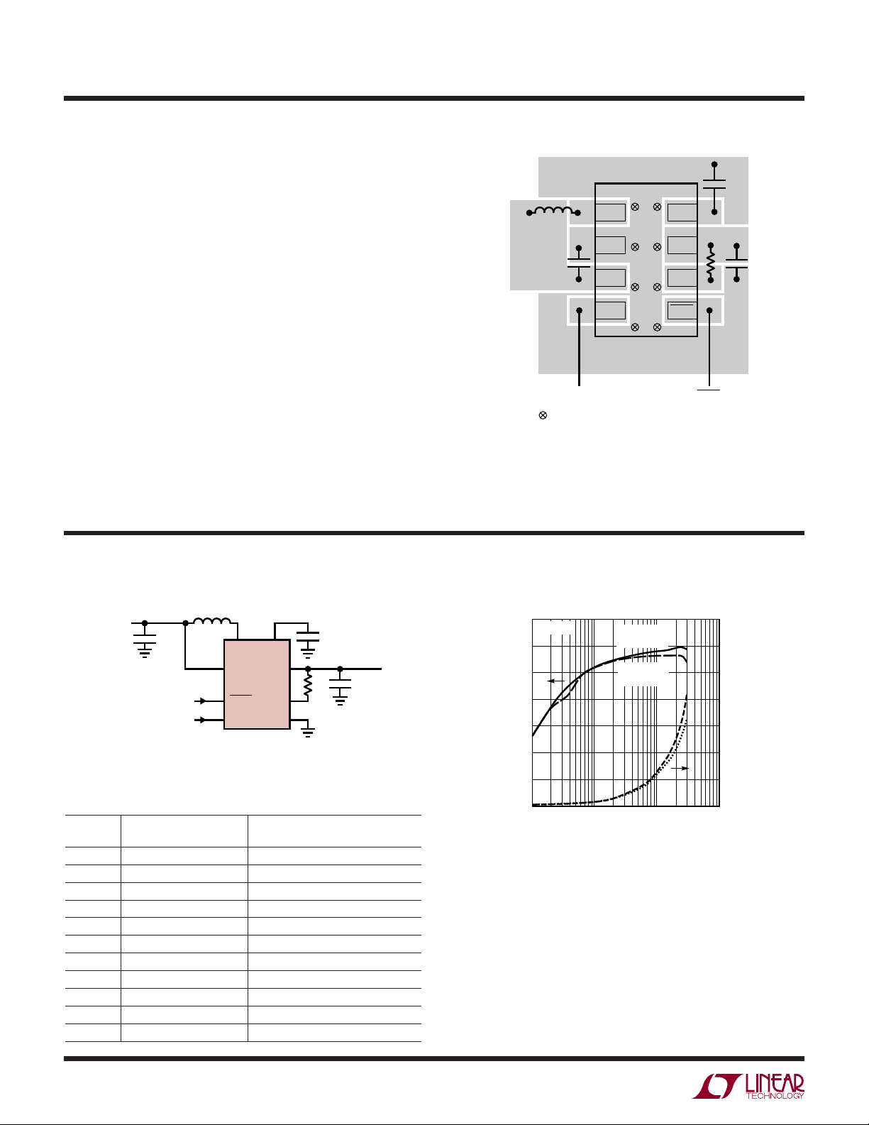
Output Voltage Ripple vs Load Current
15
100MHz MEASUREMENT BW
10
5
PEAK-TO-PEAK RIPPLE (mV)
OUT
V
0
0.1
1 10 100
LOAD CURRENT (mA)
3494 F06c
Effi ciency and Power Loss vs Load Current
80
LOAD FROM CAPACITOR
75
70
65
60
55
EFFICIENCY (%)
50
45
40
0.1
R1 VALUE REQUIRED
V
OUT
(MΩ)
25 3.57 13.0
24 3.40 14.0
23 3.24 15.0
22 3.09 16.5
21 2.94 17.5
20 2.80 19.0
19 2.67 20.0
18 2.49 21.5
17 2.37 23.0
16 2.21 25.0
15 2.05 27.0
LOAD FROM V
1 10 100
LOAD CURRENT (mA)
OUT
VIN = 3.6V
= 16V
V
OUT
3494 F06b
MAXIMUM OUTPUT CURRENT AT
3V INPUT (mA)
300
250
POWER LOSS (mW)
200
150
100
50
0
RELATED PARTS
PART NUMBER DESCRIPTION COMMENTS
LT1613 550mA (I
LT1615/LT1615-1 300mA/80mA (I
LT1930/LT1930A 1A (I
Converters
LT1945 (Dual) Dual Output, Boost/Inverter, 350mA (I
Effi ciency Step-Up DC/DC Converter
LT1946/LT1946A 1.5A (ISW), 1.2MHz/2.7MHz, High Effi ciency Step-Up DC/DC
Converters
LT3467/LT3467A 1.1A (I
Converters with Soft-Start
LT3463/LT3463A Dual Output, Boost/Inverter, 250mA (ISW), Constant Off-Time, High
Effi ciency Step-Up DC/DC Converters with Integrated Schottkys
LT3471 Dual Output, Boost/Inverter, 1.3A (I
Boost-Inverting DC/DC Converter
Linear Technology Corporation
12
1630 McCarthy Blvd., Milpitas, CA 95035-7417
(408) 432-1900 ● FAX: (408) 434-0507
), 1.4MHz, High Effi ciency Step-Up DC/DC Converter VIN: 0.9V to 10V, V
SW
ThinSOT Package
), High Effi ciency Step-Up DC/DC Converters VIN: 1V to 15V, V
SW
ThinSOT Package
), 1.2MHz/2.2MHz, High Effi ciency Step-Up DC/DC
SW
VIN: 2.6V to 16V, V
ThinSOT Package
), Constant Off-Time, High
SW
VIN: 1.2V to 15V, V
10-Lead MS Package
VIN: 2.45V to 16V, V
8-Lead MS Package
), 1.3MHz/2.1MHz, High Effi ciency Step-Up DC/DC
SW
VIN: 2.4V to 16V, V
ThinSOT Package
V
IN
DFN Package
), High Effi ciency
SW
VIN: 2.4V to 16V, V
DFN Package
●
www.linear.com
: 2.3V to 15V, V
= 34V, IQ = 3mA, ISD < 1μA,
OUT(MAX)
= 34V, IQ = 20μA, ISD < 1μA,
OUT(MAX)
= 34V, IQ = 4.2A/5.5mA, ISD < 1μA,
OUT(MAX)
= ±34V, IQ = 40μA, ISD < 1μA,
OUT(MAX)
= 34V, IQ = 3.2mA, ISD < 1μA,
OUT(MAX)
= 40V, IQ = 1.2mA, ISD < 1μA,
OUT(MAX)
= ±40V, IQ = 40μA, ISD < 1μA,
OUT(MAX)
= ±40V, IQ = 2.5mA, ISD < 1μA,
OUT(MAX)
© LINEAR TECHNOLOGY CORPORATION 2006
3494fb
LT 0507 REV B • PRINTED IN USA
 Loading...