

FEATURES
LT3486
Dual 1.3A White LED
Step-Up Converters with
Wide Dimming
U
DESCRIPTIO
■
Wide (1000:1) PWM Dimming Range with No
ColorShift
■
Independent Dimming and Shutdown Control of the
LED Drivers
■
Drives Up to 16 White LEDs at 25mA (8 per Driver)
from a Single Li-Ion Cell
■
Drives Up to 16 White LEDs at 100mA (8 per Driver)
from 12V Supply
■
±3% LED Current Programming Accuracy
■
Open LED Protection: 36V Clamp Voltage
■
Fixed Frequency Operation: Up to 2.5MHz
■
Wide Input Voltage Range: 2.5V to 24V
■
Low Shutdown Current: I
■
Overtemperature Protection
■
Available in (5mm × 3mm × 0.75mm) 16-Pin DFN
CC
< 1µA
and 16-Pin Thermally Enhanced TSSOP Packages
U
APPLICATIO S
■
Notebook PC Display
■
LED Camera Light for Cell Phones
■
Car Dashboard Lighting
■
Avionics Displays
The LT®3486 is a dual step-up DC/DC converter
specifi cally designed to drive up to 16 White LEDs (8 in
series per converter) at constant current from a single
Li-Ion cell. Series connection of the LEDs provides identical LED currents resulting in uniform brightness. The two
independent converters are capable of driving asymmetric
LED strings.
The dimming of the two LED strings can be controlled
independently via the respective CTRL pins. An internal
dimming system allows the dimming range to be extended
up to 1000:1 by feeding a PWM signal to the respective
PWM pins. The LT3486 operating frequency can be set with
an external resistor over a 200kHz to 2.5MHz range. A low
200mV feedback voltage (±3% accuracy) minimizes power
loss in the current setting resistor for better effi ciency.
Additional features include output voltage limiting when
LEDs are disconnected and overtemperature protection.
The LT3486 is available in a space saving 16-pin DFN
(5mm × 3mm × 0.75mm) and 16-pin thermally enhanced
TSSOP packages.
, LT, LTC and LTM are registered trademarks of Linear Technology Corporation.
All other trademarks are the property of their respective owners.
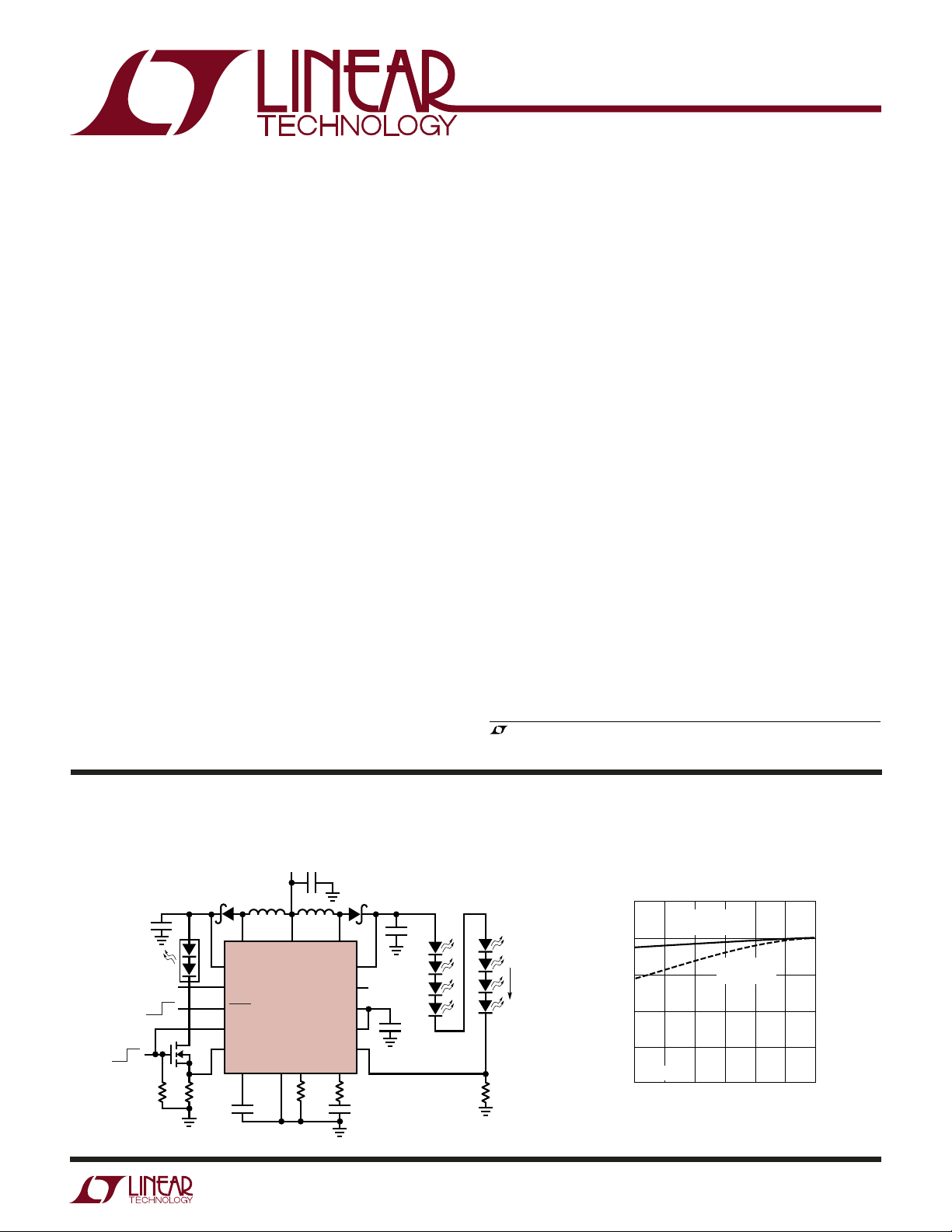
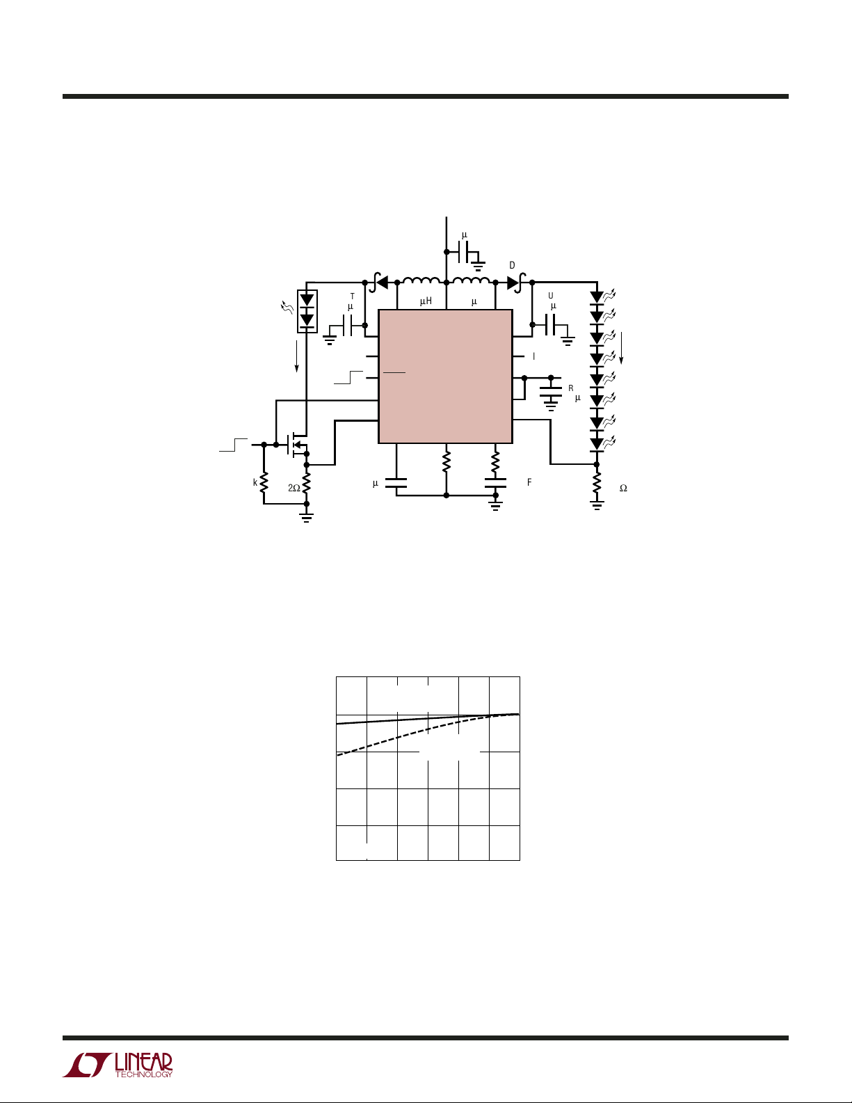
TYPICAL APPLICATIO
Li-Ion Powered Driver for Camera Flash and LCD Backlighting
V
IN
3V TO 4.2V
2.2µF
AOT3218
OFF ON
LED1
DIMMING 1
OFF ON
100k
R
FB1
0.62Ω
L1
10µHL210µH
SW1 SW2
OVP1
CTRL1
SHDN
PWM1
FB1
V
V
IN
LT3486
C1
0.1µF
RTGND
10µF
63.4k
U
CTRL2
PWM2
OVP2
REF
FB2
V
C2
2.8k
4.7nF
DIMMING 2
2.2µF
0.1µF
R
FB2
8.06Ω
3486 TA01a
8 LEDs
25mA
90
85
80
75
EFFICIENCY (%)
70
8 LEDS/25mA
65
3
Effi ciency vs V
MOVIE MODE
= 175mA
I
LED1
I
3.4 3.6 3.8
3.2
VIN (V)
FLASH MODE
= 320mA
LED1
IN
4 4.2
3486 TA01b
3486fa
1
LT3486
WW
W
ABSOLUTE AXI U RATI GS
U
(Note 1)
Input Voltage (VIN) ...................................................25V
⎯S⎯H⎯D⎯
N Voltage ..........................................................25V
SW1, SW2 Voltages .................................................40V
OVP1, OVP2 Voltages ...............................................40V
CTRL1, CTRL2 Voltages ...........................................10V
PWM1, PWM2 Voltages ...........................................10V
FB1, FB2 Voltages .....................................................10V
UUW
FOR ATIOPACKAGE/ORDER I
SW1
1
V
2
IN
OVP1
3
R
4
T
V
5
C1
FB1
6
CTRL1
7
PWM1
8
16-LEAD (5mm × 3mm) PLASTIC DFN
T
JMAX
DHC PACKAGE
EXPOSED PAD (PIN 17) IS GND
MUST BE SOLDERED TO PCB
= 125°C, θJA = 43°C/W, θJC = 4°C/W
16
SW2
15
REF
14
OVP2
13
17
SHDN
12
V
FB2
11
CTRL2
10
PWM2
9
C2
ORDER PART
NUMBER
LT3486EDHC
DHC PART
MARKING
3486
Operating Temperature Range (Note 2) ...–40°C to 85°C
Storage Temperature Range
DFN ...................................................– 65°C to 125°C
TSSOP ............................................... –65°C to 150°C
Maximum Junction Temperature .......................... 125°C
Lead Temperature (Soldering, 10sec, TSSOP) ...... 300°C
TOP VIEW
1
SW1
2
V
IN
3
OVP1
4
R
T
V
C1
FB1
CTRL1
PWM1
EXPOSED PAD IS GND (PIN 17)
MUST BE SOLDERED TO PCB
= 125°C, θJA = 38°C/W, θJC = 10°C/W
T
JMAX
17
5
6
7
8
FE PACKAGE
16-LEAD PLASTIC TSSOP
16
SW2
15
REF
14
OVP2
SHDN
13
V
12
C2
FB2
11
CTRL2
10
PWM2
9
ORDER PART
NUMBER
LT3486EFE
FE PART
MARKING
3486EFE
Order Options Tape and Reel: Add #TR
Lead Free: Add #PBF Lead Free Tape and Reel: Add #TRPBF
Lead Free Part Marking: http://www.linear.com/leadfree/
Consult LTC Marketing for parts specifi ed with wider operating temperature ranges.
The
ELECTRICAL CHARACTERISTICS
temperature range, otherwise specifi cations are at T
= 3V, unless otherwise noted.
V
SHDN
= 25°C. VIN = 3V, V
A
●
denotes the specifi cations which apply over the full operating
CTRL1
= 3V, V
CTRL2
= 3V, V
PWM1
= 3V, V
PWM2
= 3V,
PARAMETER CONDITIONS MIN TYP MAX UNITS
Minimum Operating Voltage 2.5 V
Maximum Operating Voltage 24 V
●
Feedback Voltage (FB1, FB2)
194 200 206 mV
Offset between FB1 and FB2 VOS = |FB1-FB2| 0 3 6 mV
Feedback Pin Bias Current (FB1, FB2) V
Quiescent Current V
= V
FB1
FB1
⎯S⎯H⎯D⎯
= 0.2V (Note 3) 10 45 100 nA
FB2
= V
= 1V 9 14 mA
FB2
N = 0V, CTRL1 = CTRL2 = 0V 0.1 1 µA
Switching Frequency RT = 53.6k 0.75 1 1.25 MHz
R
= 20.5k
T
●
1.7 2.2 2.7 MHz
Oscillator Frequency Range (Typical Value) (Note 4) 200 2500 kHz
Nominal RT Pin Voltage RT = 53.6k 0.54 V
2
3486fa
LT3486
The
ELECTRICAL CHARACTERISTICS
temperature range, otherwise specifi cations are at T
= 3V, unless otherwise noted.
V
SHDN
= 25°C. VIN = 3V, V
A
●
denotes the specifi cations which apply over the full operating
CTRL1
= 3V, V
CTRL2
= 3V, V
PWM1
= 3V, V
PWM2
= 3V,
PARAMETER CONDITIONS MIN TYP MAX UNITS
Maximum Duty Cycle R
R
R
= 53.6k
T
= 20.5k 90 %
T
= 309k 98 %
T
●
90 96 %
Switch Current Limit (SW1, SW2) 1 1.3 A
Switch V
Switch Leakage Current V
I
CESAT
SW1
SW1
= I
= 0.75A 300 mV
SW2
= V
= 10V 0.1 5 µA
SW2
Error Amplifi er Transconductance ∆I = ±5µA 220 µA/V
Error Amplifi er Voltage Gain 120
VC1, VC2 Switching Threshold 0.85 V
VC1, VC2 Clamp Voltage 1.5 V
VC1, VC2 Source Current V
VC1, VC2 Sink Current V
VC1, VC2 Pin Leakage Current VC1 = VC2 = 1V, V
FB1
FB1
= V
= 0V 25 µA
FB2
= V
= 1V 25 µA
FB2
PWM1
= V
= 0V 1 10 nA
PWM2
OVP1, OVP2 Overvoltage Threshold Voltage 34 36 38 V
CTRL1, CTRL2 Voltages to Turn Off LED1, 2 Currents
●
75 mV
CTRL1, CTRL2 Voltages to Turn On LED1, 2 Currents 150 mV
CTRL1, CTRL2 Voltages for Full LED1, 2 Currents 1.8 V
CTRL1, CTRL2 Pin Bias Current V
PWM1, PWM2 Voltage High
PWM1, PWM2 Voltage Low
PWM1, PWM2 Pin Bias Current V
CTRL1
PWM1
= V
= V
= 3V
CTRL2
= 3V 0.1 1 µA
PWM2
●
20 30 40 µA
●
0.9 V
●
0.4 V
SHDN Voltage High 1.6 V
SHDN Voltage Low 0.4 V
SHDN Pin Bias Current V
REF Voltage I
REF Source Current
= 3V 20 µA
SHDN
= 10µA 1.2 1.25 1.3 V
REF
●
50 80 µA
Note 1: Stresses beyond those listed under Absolute Maximum Ratings
may cause permanent damage to the device. Exposure to any Absolute
Maximum Rating condition for extended periods may affect device
reliability and lifetime.
Note 2: The LT3486E is guaranteed to meet specifi ed performance from
0°C to 70°C and is designed, characterized and expected to meet these
extended temperature limits, but is not tested at –40°C and 85°C.
Note 3: Current fl ows out of the pin.
Note 4: Guaranteed by design and test correlation, not production tested.
3486fa
3
LT3486
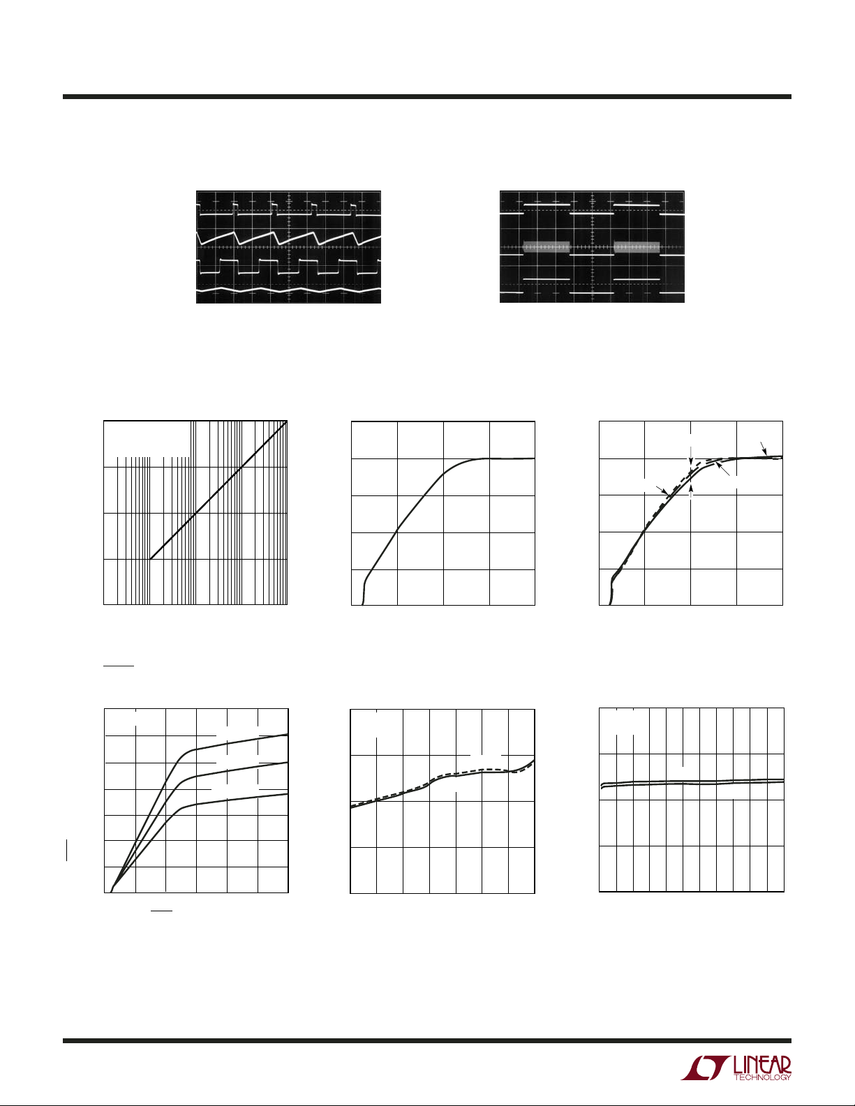
TYPICAL PERFOR
Switching Waveforms PWM Dimming Wavforms
UW
CE CHARACTERISTICSA
TA = 25°C unless otherwise specifi ed.
V
SW2
50V/DIV
I
L2
500mA/DIV
V
SW1
10V/DIV
I
L1
1A/DIV
VIN = 3.6V
8 LEDs/25mA
2 LEDs/320mA
CIRCUIT OF FRONT PAGE APPLICATION
LED Current vs PWM Duty Cycle
Wide Dimming Range (1000:1)
100
VIN = 12V
8/8 LEDs
PWM FREQ = 100Hz
10
(mA)
1
LED
I
0.1
0.01
0.01 1 10 100
0.1
PWM DUTY CYCLE (%)
0.5µs/DIV
3486 G01
3486 G17
vs V
V
FB
CTRL
250
VIN = 3.6V
= 25°C
T
A
200
150
100
FEEDBACK VOLTAGE (mV)
50
0
0
0.5
CONTROL VOLTAGE (V)
200mA/DIV
500mA/DIV
1
I
LED
PWM
5V/DIV
1.5
I
L
VIN = 12V
8/8 LEDs
PWM FREQ = 1kHz
2
3486 G03
0.2ms/DIV
VFB vs V
3486 G18
CTRL
(Temperature Variation)
250
200
TA = –50°C
150
100
FEEDBACK VOLTAGE (mV)
50
0
0
0.5
CONTROL VOLTAGE (V)
± 5mV
1
TA = 85°C
TA = 25°C
1.5
2
3486 G04
SHDN Pin Bias Current
(CTRL1 = CTRL2 = 3V)
140
VIN = 3.6V
120
100
80
60
40
SHDN PIN BIAS CURRENT (µA)
20
0
01220
48
SHDN PIN VOLTAGE (V)
TA = 50°C
TA = 25°C
TA = 100°C
16 24
4
3486 G05
Open-Circuit Output Clamp
Voltage vs Temperature
37
= 3.6V
V
IN
= 63.4k
R
T
36
35
34
OUTPUT CLAMP VOLTAGE (V)
33
–50
–25 0 25 50
TEMPERATURE (°C)
V
OUT1
V
OUT2
75 100 125
3486 G06
Open-Circuit Output Clamp
Voltage vs V
37
= 3.6V
V
IN
= 63.4k
R
T
36
35
34
OUTPUT CLAMP VOLTAGE (V)
33
4
2
IN
V
OUT1
6
12
8
10
V
IN
(V)
V
OUT2
18
14
16
22 24
20
3486 G07
3486fa
UW
0
TYPICAL PERFOR A CE CHARACTERISTICS
Input Current with Output 1 and
Output 2 Open Circuit
20
15
T
A
R
= 25°C
= 63.4k
T
R
vs Oscillator Frequency Oscillator Frequency vs V
T
1000
LT3486
TA = 25°C unless otherwise specifi ed.
1100
1050
R
= 53.6k
T
IN
10
INPUT CURRENT (mA)
5
0
4
6
2
12
8
10
VIN (V)
Oscillator Frequency vs
Temperature
10000
= 22.1k
R
T
= 53.6k
R
1000
OSCILLATOR FREQUENCY (kHz)
T
= 309k
R
T
100
–50
–25 0 25 50 75 100
TEMPERATURE (°C)
100
(kΩ)
T
R
10
0
14
16
18
22 24
20
3486 G08
QUIESCENT CURRENT (mA)
125
3486 G11
500 2500200015001000
OSCILLATOR FREQUENCY (kHz)
Quiescent Current vs V
12
10
8
6
4
2
0
0
UVLO
10 14 18 22 24
81216
6
4
V
IN
3486 G09
IN
SHDN = 3V
CTRL1 = CTRL2 = 3V
202
(V)
3486 G12
1000
950
OSCILLATOR FREQUENCY (kHz)
900
6
4
2
12
10
8
VIN (V)
PWM Pin Input Bias Current
1.0
V
= 3.6V
IN
0.5
PWM 1
PWM 2
4
PWM PIN CURRENT (µA)
–0.5
–1.0
0
2
0
PWM PIN VOLTAGE (V)
18
14
16
6
22 24
20
3486 G10
8
1
Switch Current Limit vs
Duty Cycle
1800
V
= 3.6V
IN
1700
1600
1500
1400
CURRENT LIMIT (mA)
1300
1200
20
40 60
30 50
DUTY CYCLE (%)
REF Voltage vs Temperature
1.30
V
= 3.6V
IN
1.28
1.26
1.24
REF VOLTAGE (V)
1.22
1.20
80
70
90
3486 G14
100
–50 –25
0
TEMPERATURE (°C)
50
25
75
100
125
3486 G15
REF Voltage Load Regulation
1.30
1.25
1.20
1.15
1.10
1.05
REF VOLTAGE (V)
1.00
0.95
V
= 3.6V
IN
T
= 25°C
A
0.90
0
40 80 120 20014020 60 100 180
REF LOAD CURRENT (µA)
TA = 25°C
TA = –50°C
TA = 85°C
160
3468 G16
3486fa
5

LT3486
PI FU CTIO S
UUU
SW1, SW2 (Pins 1, 16): The SW Pins are the Collectors
of the Internal Power Transistors. Connect the inductors
and Schottky diodes to these pins. Minimize trace area
at these pins to minimize EMI.
(Pin 2): Input Supply Pin. Must be locally bypassed
V
IN
with an X5R or X7R type ceramic capacitor.
OVP1, OVP2 (Pins 3, 14): Output Overvoltage Protection
Pins. Connect these pins to the output capacitors. The
on-chip voltage detectors monitor the voltages at these
pins and limit it to 36V (typ) by turning off the respective
switcher and pulling its V
(Pin 4): Timing Resistor to Program the Switching
R
T
Frequency. The switching frequency can be programmed
from 200kHz to 2.5MHz.
, VC2 (Pins 5, 12): The VC Pins are the Outputs of the
V
C1
Internal Error Amplifi er. The voltages at these pins control
the peak switch currents. Connect a resistor and capacitor
compensation network from these pin to ground.
FB1, FB2 (Pins 6, 11): The LT3486 regulates the voltage
at each feedback pin to 200mV. Connect the cathode of
the lowest LED in the string and the feedback resistor
) to the respective feedback pin. The LED current in
(R
FB
each string can be programmed by:
≅ 200mV/RFB, when V
I
LED
I
LED
≅ V
/(5RFB), when V
CTRL
pin low.
C
CTRL
CTRL
> 1.8V
< 1V
CTRL1, CTRL2 (Pins 7, 10): The CTRL pins are used to
provide dimming and shutdown control for the individual
switching converters. Connecting these to ground shuts
down the respective converter. As the voltages on these
pins is ramped from 0V to 1.8V, the LED current in each
converter ramps from 0 to I
age above 1.8V does not affect the LED current.
PWM1, PWM2 (Pins 8, 9): The PWM control pins can
be used to extend the dimming range for the individual
switching converter. The LED current in each string can
be controlled down to µA levels by feeding a PWM signal
to these pins. When the PWM pin voltage is taken below
0.4V, the respective converter is turned off and its V
is disconnected from the internal circuitry. Taking it higher
than 0.9V resumes normal operation. Connect these pins
to 0.9V supply or higher, if not in use.
SHDN (Pin 13): Shutdown Pin for the Device. Connect it
to 1.6V or higher to enable device; 0.4V or less to disable
device.
REF (Pin 15): The internal bandgap reference (1.25V) is
available at this pin. Bypass with a 0.1µF X5R or X7R ceramic capacitor. Draw no more than 50µA from this pin.
Exposed Pad (Pin 17): Ground. The exposed pad of the
package provides an electrical contact to ground and good
thermal connection to the printed circuit board (PCB).
Solder the exposed pad to the PCB system ground.
= (200mV/RFB). Any volt-
LED
pin
C
6
3486fa

BLOCK DIAGRA
LT3486
W
R
4
OSC
RAMP
GEN
T
OVP1
3
OVERVOLT
DETECTION
OV1
EN1
PWM
LOGIC
OSC
SW1
1
CONVERTER1 CONVERTER2
Q1 Q2
+
R
SNS1
A3
–
PWM
COMP
V
C1
5
OV1 OV2
CONVERTER1
+
A2
–
CONTROL
8
7
CTRL1PWM1 FB1
++
EA
A1 A1
0.2V
+
–
+
SHDN
20k
6
V
IN
2
OSC
REF 1.25V
START-UP
CONTROL
13
SHDN REF FB2
0.2V
15
SW2
16
DRIVER
+
A3
R
SNS2
–
PWM
COMP
+
A2
EA
+
–
–
+
EN2EN1
80k80k
20k
11
CONVERTER 2
CONTROL
10
CTRL2
PWM2
9
PWM
LOGIC
OVERVOLT
DETECTION
OSC
OV2
EN2
17
14
EXPOSED
PAD
12
3486 F01
OVP2
V
C2
Figure 1. LT3486 Block Diagram
3486fa
7

LT3486
OPERATIO
U
Main Control Loop
The LT3486 uses a constant frequency, current mode
control scheme to provide excellent line and load regulation.
It incorporates two identical, but fully independent PWM
converters. Operation can be best understood by referring
to the block diagram in Figure 1. The oscillator, start-up
bias and the bandgap reference are shared between the two
converters. The control circuitry, power switch, dimming
control etc., are all identical for both converters.
At power-up, the output capacitors of both converters are
charged up to V
(input supply voltage) via their respective
IN
inductor and the Schottky diode. If the SHDN pin is taken
above 1.6V, the bandgap reference, start-up bias and the
oscillator are turned on. Grounding the SHDN pin shuts
down the part.
The CTRL1 and CTRL2 pins perform independent dimming
and shutdown control for the two converters. Taking
the CTRL pins high, enables the respective converters.
Connecting these pins to ground, shuts down each
converter by pulling their respective V
pin low.
C
Working of the main control loop can be understood by
following the operation of converter 1. At the start of
each oscillator cycle, the power switch Q1 is turned on.
A voltage proportional to the switch current is added to
a stabilizing ramp and the resulting sum is fed into the
positive terminal of the PWM comparator A2. When this
voltage exceeds the level at the negative input of A2, the
PWM logic turns off the power switch. The level at the
negative input of A2 is set by the error amplifi er A1, and
is simply an amplifi ed version of the difference between
the feedback voltage and the 200mV reference voltage. In
this manner, the error amplifi er A1 regulates the feedback
voltage to 200mV reference voltage. The output of the
error amplifi er A1 sets the correct peak current level in
inductor L1 to keep the output in regulation. The CTRL1
pin voltage is used to adjust the reference voltage.
The PWM1, 2 control pins are used to extend the dimming
range for the individual converter. The LED current in each
string can be controlled down to µA levels by feeding
a PWM signal to these pins. Refer to the Applications
Information section for more detail.
If only one of the converters is turned on, the other converter
will stay off and its output will remain charged up to V
IN
(input supply voltage).
Minimum Output Current
The LT3486 can drive an 8-LED string at 4mA LED current
without pulse skipping. As current is further reduced, the
device may begin skipping pulses. This will result in some
low frequency ripple, although the LED current remains
regulated on an average basis down to zero. The photo
in Figure 2 shows circuit operation with 8 white LEDs
at 4mA current driven from 3.6V supply. Peak inductor
current is less than 200mA and the regulator operates in
discontinuous mode implying that the inductor current
reached zero during the discharge phase. After the inductor
current reaches zero, the switch pin exhibits ringing due to
the LC tank circuit formed by the inductor in combination
with switch and diode capacitance. This ringing is not
harmful; far less spectral energy is contained in the ringing
than in the switch transitions. The ringing can be damped
by application of a 300Ω resistor across the inductors,
although this will degrade effi ciency.
V
OUT2
10mV/DIV
V
SW2
20V/DIV
I
L2
200mA/DIV
VIN = 3.6V
= 4mA (8 LEDs)
I
LED2
CIRCUIT OF FRONT PAGE APPLICATION
Figure 2. Switching Waveforms
0.5µs/DIV
3486 F02
Open-Circuit Protection
The LT3486 has internal open-circuit protection for both
the converters. Connect the overvoltage protection pins
(OVP1, OVP2) to the output of the respective converter.
When the LEDs are disconnected from the circuit or fail
open, the on-chip voltage detectors monitor the voltages at
the OVP1 and OVP2 pins and limits these voltages to 36V
(typ) by turning off the respective switcher. The converter
will then switch at a very low frequency to minimize the
input current. Output voltage and input current during
3486fa
8

OPERATIO
LT3486
U
output open circuit are shown in the Typical Performance
Characteristics graphs.
Figure 3a shows the transient response of switcher 1 with
the LEDs disconnected from the output. When the LED1
string is disconnected from the output, the voltage at
the feedback pin (FB1) drops to 0V. As a result, the error
amplifi er charges up the V
node to the clamp voltage
C
level of 1.5V (typ). The converter starts switching at peak
current limit and ramps up the output voltage. When the
output voltage reaches the OVP clamp voltage level of
36V (typ), the LT3486 shuts off the converter by pulling
node to ground. The converter then regulates the
the V
C
output voltage at 36V (typ) by switching at a very low
frequency.
In the event one of the converters has an output opencircuit, its output voltage will be clamped at 36V (typ).
However, the other converter will continue functioning
properly. The photo in Figure 3b shows circuit operation
with converter 1 output open-circuit and converter 2 driving
I
L1
1A/DIV
eight LEDs at 25mA. Converter 1 starts switching at a very
low frequency, reducing its input current.
Soft-Start
The LT3486 has a separate internal soft-start circuitry for
each converter. Soft-start helps to limit the inrush current
during start-up. Soft-start is achieved by clamping the
output of the error amplifi er during the soft-start period.
This limits the peak inductor current and ramps up the
output voltage in a controlled manner.
The converter enters into soft-start mode whenever the
respective CTRL pin is pulled from low to high. Figure 4
shows the start-up waveforms with converter 2 driving
eight LEDs at 25mA. The fi ltered input current, as shown
in Figure 4, is well controlled. The soft-start circuit is more
effective when driving a smaller number of LEDs.
Undervoltage Lockout
The LT3486 has an undervoltage lockout circuit which
shuts down both the converters when the input voltage
drops below 2.1V (typ). This prevents the converter to
operate in an erratic mode when powered from low supply
voltages.
V
OUT1
20V/DIV
Overtemperature Protection
The maximum allowable junction temperature for LT3486 is
V
C1
2V/DIV
VIN = 3.6V
CIRCUIT OF
FRONT PAGE
APPLICATION
100µs/DIV
LED1 DISCONNECTED
AT THIS INSTANT
3486 F03a
Figure 3a. Transient Response of Switcher 1 with LED1
Disconnected from the Output
I
L1
1A/DIV
V
OUT1
1V/DIV
AC COUPLED
I
L2
500mA/DIV
VIN = 3.6V
CIRCUIT OF FRONT PAGE APPLICATION
LED1 DISCONNECTED
2ms/DIV
3486 F03b
Figure 3b. Switching Waveforms with Output 1 Open Circuit Figure 4. Start-Up Waveforms
125°C. In normal operation, the IC’s junction temperature
should be kept below 125°C at an ambient temperature of
85°C or less. If the junction temperature exceeds 150°C, the
internal thermal shutdown circuitry kicks in and turns-off
both the converters. The converters will remain off until
the die temperature falls below 150°C.
I
IN
200mA/DIV
V
OUT2
10V/DIV
V
FB2
200mV/DIV
CTRL2
5V/DIV
VIN = 3.6V
8 LEDs, 25mA
CIRCUIT OF FRONT PAGE APPLICATION
0.5ms/DIV
3486 F04
3486fa
9

LT3486
U
WUU
APPLICATIO S I FOR ATIO
Duty Cycle
The duty cycle for a step-up converter is given by:
VVV
++–
D
where:
V
OUT
V
D
V
CESAT
V
IN
The maximum duty cycle achievable for LT3486 is 96%
(typ) when running at 1MHz switching frequency. It increases to 98% (typ) when run at 200kHz and drops to
90% (typ) at 2MHz. Always ensure that the converter is
not duty-cycle limited when powering the LEDs at a given
switching frequency.
Setting the Switching Frequency
OUT D IN
=
VVV
OUT D CESAT
–
= Output voltage
= Schottky forward voltage drop
= Saturation voltage of the switch
= Input battery voltage
Operating Frequency Selection
The choice of operating frequency is determined by several factors. There is a tradeoff between effi ciency and
component size. Higher switching frequency allows the
use of smaller inductors albeit at the cost of increased
switching losses and decreased effi ciency.
Another consideration is the maximum duty cycle
achievable. In certain applications the converter needs to
operate at the maximum duty cycle in order to light up
the maximum number of LEDs. The LT3486 has a fi xed
oscillator off-time and a variable on-time. As a result, the
maximum duty cycle increases as the switching frequency
is decreased.
The circuit of Figure 6a is operated with different values of
timing resistor (R
at 800kHz (R
= 21.5k). The CTRL pins are used to provide dimming
(R
T
). RT is chosen so as to run the converters
T
= 63.4k), 1.25MHz (RT = 39.1k) and 2MHz
T
for the respective LED strings. The effi ciency comparison
for different R
values is shown in Figure 6b.
T
The LT3486 uses a constant frequency architecture that
can be programmed over a 200kHz to 2.5MHz range
with a single external timing resistor from the R
ground. The nominal voltage on the R
pin is 0.54V, and the
T
pin to
T
current that fl ows into the timing resistor is used to charge
and discharge an internal oscillator capacitor. A graph for
selecting the value of R
for a given operating frequency
T
is shown in the Figure 5.
1000
100
(kΩ)
T
R
10
0
500 2500200015001000
OSCILLATOR FREQUENCY (kHz)
3486 G09
D1 D2
C
OUT1
2.2µF
SW1 SW2V
, C
REF
OUT2
OVP1
CTRL1
SHDN
PWM1
FB1
V
C1
: 35V, X5R
25mA
OFF ON
CIN: 10V, X7R
C
OUT1
D1, D2: ZETEX ZHCS400
L1, L2: TOKO D53LC TYPE A
Figure 6a. 5V to 8/8 White LEDs
C
IN
5V
10µF
L1
10µH
2.8k 2.8k
4.7nF 4.7nF
IN
LT3486
GND
L2
10µH
R
T
CTRL2
PWM2
R
T
OVP2
REF
FB2
V
C2
C
OUT2
2.2µF
25mA
1.25V
C
REF
0.1µF
8.06Ω8.06Ω
3486 F06a
10
Figure 5. Timing Resistor (RT) Value
3486fa

LT3486
U
WUU
APPLICATIO S I FOR ATIO
90
VIN = 5V
8/8 LEDs
80
70
60
EFFICIENCY (%)
50
40
30
0
Figure 6b. Effi ciency Comparison for Different RT Resistors
Inductor Selection
The choice of the inductor will depend on the selection of
switching frequency of LT3486. The switching frequency
can be programmed from 200kHz to 2.5MHz. Higher
switching frequency allows the use of smaller inductors
albeit at the cost of increased switching losses.
The inductor current ripple (ΔI
the Schottky diode and the switch, is given by:
VV V
IN MIN OUT MAX IN MIN
∆=
I
L
() ( ) ()
where:
L = Inductor
f = Operating frequency
V
V
The ΔI
= Minimum input voltage
IN(MIN)
OUT(MAX)
= Maximum output voltage
is typically set to 20% to 40% of the maximum
L
inductor current.
The inductor should have a saturation current rating greater
than the peak inductor current required for the application.
Also, ensure that the inductor has a low DCR (copper wire
resistance) to minimize I
inductor values range from 4.7µH to 22µH.
RT = 63.4k
RT = 21.5k
RT = 39.1k
5101520
LED CURRENT (mA)
), neglecting the drop across
L
•–
()
VfL
OUT MAX
••
()
2
R power losses. Recommended
25
3486 F06b
Several inductors that work well with the LT3486 are listed
in Table 1. Consult each manufacturer for more detailed information and for their entire selection of related parts.
Table 1. Recommended Inductors
MAX CURRENT
L DCR RATING
PART (µH) (Ω) (A) VENDOR
LQH55DN150M 15 0.150 1.40 Murata
LQH55DN220M 22 0.190 1.20 (814) 237-1431
www.murata.com
A915AY-4R7M 4.7 0.045 2.49 Toko
A915AY-6R8M 6.8 0.068 2.01 (847) 297-0070
A915AY-100M 10 0.090 1.77 www.toko.com
A918CY-100M 10 0.098 1.22
A918CY-150M 15 0.149 0.94
CDRH4D28-100 10 0.048 1.30 Sumida
CDRH5D18-150 15 0.145 0.97 (847) 956-0666
www.sumida.com
Capacitor Selection
The small size of ceramic capacitors make them ideal
for LT3486 applications. Use only X5R and X7R types
because they retain their capacitance over wider voltage
and temperature ranges than other types such as Y5V
or Z5U. A 4.7µF or larger input capacitor is suffi cient for
most applications. Always use a capacitor with suffi cient
voltage rating.
Table 2 shows a list of several ceramic capacitor manufacturers. Consult the manufacturers for detailed information
on their entire selection of ceramic parts.
Table 2. Ceramic Capacitor Manufacturers
Taiyo Yuden (408) 573-4150
www.t-yuden.com
AVX (803) 448-9411
www.avxcorp.com
Murata (714) 852-2001
www.murata.com
Diode Selection
Schottky diodes with their low forward voltage drop and
fast reverse recovery, are the ideal choices for LT3486
applications. The diode conducts current only during the
switch off time. The peak reverse voltage that the diode
must withstand is equal to the regulator output voltage.
3486fa
11

LT3486
U
WUU
APPLICATIO S I FOR ATIO
The average forward current in normal operation is equal
to the output current, and the peak current is equal to the
peak inductor current. A Schottky diode rated at 1A is suffi cient for most LT3486 applications. Some recommended
Schottky diodes are listed in Table 3.
Table 3. Recommended Schottky Diodes
PART NUMBER VR (V) I
MBR0530 30 0.5 On Semiconductor
MBRM120E 20 1 www.onsemi.com
ZLLS400 40 0.4 Zetex
ZLLS1000 40 1 www.zetex.com
ZHCS400 40 0.4
ZHCS1000 40 1
When the LT3486 is set up for PWM dimming operation,
choose a Schottky diode with low reverse leakage current.
During PWM dimming operation, the output capacitor is
required to hold up the charge in the PWM “off” period.
A low reverse leakage Schottky helps in that mode of operation. The Zetex ZLLS400 and ZLLS1000 are available
in a small surface mount package and are a good fi t for
this application.
MOSFET Selection
(A) MANUFACTURER
AVG
200
R
FB
1
R
FB
2
Table 4. RFB Value Selection
I
5 40.2
10 20.0
15 13.3
20 10.0
25 8.06
mV
=
I
LED
1
200
mV
=
I
LED
2
(mA) RFB (Ω)
LED
Most low power white LEDs are driven at maximum currents of 15mA to 25mA. The LT3486 can be used to power
high power LEDs as well. Refer to the Typical Applications
for more detail.
Dimming Control
The dimming of the two LED strings can be controlled
independently by modulating the respective CTRL and
PWM pins. There are two ways to control the intensity
of the LEDs.
The power MOSFET used in LT3486 applications with wide
dimming range requirements should be chosen based on
the maximum drain-source voltage. The maximum drain
current I
D(MAX)
and gate-to-source voltages should also
be considered when choosing the FET.
Choose a MOSFET with maximum V
(drain source) volt-
DS
age greater than the output clamp voltage i.e., 36V (typ).
Fairchild Semiconductor’s FDN5630 (60V, 1.7A N-channel
FET) is a good fi t for most LT3486 applications. For dimming low current LEDs (~25mA), Fairchild 2N7002 is a
good alternative.
Programming LED Current
The current in each LED string can be set independently
by the choice of resistors R
FB1
and R
respectively
FB2
(see front page application). The feedback reference is
200mV. In order to have accurate LED current, precision
resistors are preferred (1% is recommended).
Adjusting the LED Current Value
Controlling the current fl owing through the LEDs controls
the intensity of the LEDs.This is the easiest way to control
the intensity of the LEDs. The LED forward current can be
controlled by modulating the DC voltage at the respective
CRTL pin. The PWM pins are not in use when appying
this scheme. They must be connected to a 0.9V supply or
higher. The DC voltage at the CTRL pin can be modulated
in two ways.
(a) Using a DC Voltage Source
For some applications, the preferred method of brightness
control is a variable DC voltage fed to the CTRL pins. The
CTRL1, CTRL2 pin voltage can be modulated to set the
dimming of the respective LED string. As the voltage on
the CTRL1, CTRL2 pin increases from 0V to 1.8V, the LED
current increases from 0 to I
. As the CTRL1, CTRL2
LED
pin voltage increases beyond 1.8V, it has no effect on the
LED current.
3486fa
12

LT3486
3486 F07
C1
1µF
PWM
10kHz TYP
R1
10k
LT3486
CTRL1,2
U
WUU
APPLICATIO S I FOR ATIO
The LED current can be set by:
≈ (200mV/RFB), when V
I
LED
I
LED
≈ (V
/5 • RFB), when V
CTRL
Feedback voltage variation versus control voltage is given
in the Typical Performance Characteristics graphs.
(b) Using a Filtered PWM Signal
A variable duty cycle PWM can be used to control the
brightness of the LED string. The PWM signal is fi ltered
(Figure 7) by an RC network and fed to the CTRL1, CTRL2
pins.
The corner frequency of R1, C1 should be much lower
than the frequency of the PWM signal. R1 needs to be
much smaller than the internal impedance in the CTRL
pins, which is 100kΩ.
CTRL
CTRL
> 1.8V
< 1V
Pulse-Width Modulation (PWM)
Adjusting the forward current fl owing in the LEDs changes
the intensity of the LEDs, as explained in the previous section. However, a change in forward current also changes the
color of the LEDs. The chromaticity of the LEDs changes
with the change in forward current. Many applications cannot tolerate any shift in the color of the LEDs. Controlling
the intensity of the LEDs via applying a PWM signal allows
dimming of the LEDs without changing the color.
Dimming the LEDs via a PWM signal essentially involves
turning the LEDs on and off at the PWM frequency. The
human eye has a limit of 60 frames per second. By increasing the PWM frequency to say, 80Hz, the eye can
be deceived into believing that the pulsed light source is
continously on. Additionally by modulating the duty cycle
(amount of “on-time”), the intensity of the LEDs can be
controlled. The color of the LEDs remains unchanged in
this scheme since the LED current value is either zero or
a constant value.
Figure 7. Dimming Control Using a Filtered PWM Signal
12V (TYP)
9V TO 15V
L1
10µH
C
OUT1
D1
2.2µF
LUXEON
LEDs
LXCL-PWF1
100mA
DIMMING
INPUT 1
PWM
FREQ
1kHz
100k 100k
OFF ON
Q1
R
C
FB1
OUT1
2Ω
C
IN
C1: 10V, X5R OR X7R
C
REF
SW1 SW2
OVP1
V
CTRL1
IN
SHDN
PWM1
FB1
V
C1
3.65k
2.2nF
, C
: 35V, X5R OR X7R
OUT2
: 25V, X5R OR X7R
: 6.3V, X5R OR X7R
LT3486
21.5k
C
IN
10µF
L2
µH
10
5V
V
R
C1 1µF
IN
T
D2
OVP2
CTRL2
REF
PWM2
FB2
V
C2
22pF
3.65k
2.2nF
D1, D2: ZETEX ZLLS1000
L1, L2: TOKO D53LC (TYPE A)
Q1, Q2: FAIRCHILD FDN5630
C
OUT2
2.2µF
V
IN
C
REF
0.1µF
Figure 8(a) shows a 12V to 8/8 white LED driver. The PWM
dimming control method requires an external NMOS tied
to the cathode of the lowest LED in the string, as shown in
LUXEON
LEDs
LXCL-PWF1
100mA
DIMMING
INPUT 2
Q2
R
FB2
2Ω
3486 TA10a
PWM
FREQ
1kHz
I
LED
200mA/DIV
I
L
500mA/DIV
PWM
5V/DIV
VIN = 12V
8/8 LEDs
PWM FREQ = 1kHz
0.2ms/DIV
Figure 8b. PWM Dimming Waveforms
3486 G18
Figure 8a. 12V to 8/8 White LEDs
3486fa
13

LT3486
U
WUU
S I FOR ATIOAPPLICATIO
the fi gure. A PWM logic input is applied to the gate of the
NMOS and the PWM pin of the LT3486. When the PWM
input is taken high, the LEDs are connected to the R
resistor and a current I
= 200mV/RFB fl ows through
LED
the LEDs. When the PWM input is taken low, the LEDs are
disconnected and turn off. The low PWM input applied to
the LT3486 ensures that the respective converter turns
off and its V
the capacitor connected to the V
pin goes high impedance. This ensures that
C
pin retains its voltage
C
which in turn allows the LEDs to turn on faster, as shown
in Figure 8(b). The CTRL pin is not used to modulate the
LED current in the scheme. It can be connected to a supply
voltage greater than 1.8V.
The dimming control pins (PWM1, PWM2) can be used
to extend the dimming range for the individual switching
converters. The LED current can be controlled down to
µA levels by feeding a PWM signal with frequencies in the
range of 80Hz to 50kHz. The LED current can be controlled
by PWM frequencies above 50kHz but the controllable
current decreases with increasing frequency. Pulling the
PWM pins below 0.4V disables the respective switcher.
Taking it higher than 0.9V resumes normal operation.
Connect these pins to 0.9V or higher if not in use.
FB
Figure 9 shows the LED current variation vs PWM duty
cycle. The LED current is controlled by applying a PWM
of frequency 100Hz, 1kHz and 25kHz to the circuit of
Figure 8a. As seen in the curves, the LED string is able to
get a wide (1000:1) dimming range with PWM frequency of
100Hz. The dimming range decreases as PWM frequency
goes up.
Board Layout Consideration
As with all switching regulators, careful attention must be
paid to the PCB board layout and component placement.
To prevent electromagnetic interference (EMI) problems,
proper layout of high frequency switching paths is essential.
Minimize the length and area of all traces connected to the
switching node pins (SW1 and SW2). Keep the feedback
pins (FB1 and FB2) away from the switching nodes.
The DFN and FE packages both have an exposed paddle
that must be connected to the system ground. The ground
connection for the feedback resistors should be tied directly
to the ground plane and not shared with any other component, except the R
resistor, ensuring a clean, noise-free
T
connection. Recommended component placement for the
DFN package is shown in the Figure 10.
100
10
1
LED CURRENT (mA)
0.1
PWM FREQ = 100Hz
PWM FREQ = 1kHz
0.01
0.01 1 10 100
0.1
PWM DUTY CYCLE (%)
PWM FREQ = 25kHz
3486 F09
Figure 9. LED Current Variation vs PWM Duty Cycle
LED1
VIAs TO VIN PLANE
V
OVP1
R
V
PWM1
OUT1
T
C1
FB1
CTRL1 CTRL2
PLANE
IN
SW1 SW2
V
IN
16
1
15
2
14
3
17
13
4
12
5
11
6
10
7
9
8
V
IN
Figure 10. Recommended Layout for LT3486
V
OUT2
V
IN
VIAs TO GROUND PLANEVIAs TO V
LED2
OVP2
SHDN
PWM2
REF
V
C2
FB2
3486 F10
3486fa
14
TYPICAL APPLICATIO S
Li-Ion Cell Powered Driver for Camera Flash and LCD Backlighting
U
V
IN
3V TO 5V
C
10mF
LT3486
IN
0V
OFF ON
LED1
AOT3218
5V
100k
C
OUT1
2.2mF
320mA
OFF ON
Q1
R
FB1
0.62
W
C
: 6.3V, X5R OR X7R DIELECTRIC
IN
, C
C
OUT1
D1: ZETEX ZHCS1000
D2: ZETEX ZHCS400
: 35V, X5R OR X7R
OUT2
D1
L1
10mH
SW1 SW2
OVP1
CTRL1
SHDN
PWM1
FB1
V
0.1mF
LT3486
C1
63.4k
Effi ciency vs V
D2
L2
10mH
V
IN
OVP2
CTRL2
PWM2
R
T
L1, L2: TOKO D53LC (TYPE A)
Q1: FAIRCHILD FDN5630
DIMMING 2DIMMING 1
REF
FB2
V
C2
2.8k
4.7nF
IN
C
OUT2
2.2mF
C
REF
0.1mF
R
FB2
8.06
3486 TA02a
25mA
W
90
85
80
75
EFFICIENCY (%)
70
8 LEDS/25mA
65
3
3.2
MOVIE MODE
= 175mA
I
LED1
FLASH MODE
= 320mA
I
LED1
3.4 3.6 3.8
VIN (V)
4 4.2
3486 TA01b
3486fa
15

LT3486
LED C
Effi ci
PWM Duty Cycl
Wide (250:1) Dimmi
PWM Dimmi
TYPICAL APPLICATIO S
U
1 Li-Ion Cell to 8/8 White LEDs
3V TO 5V
C
IN
10µF
urrent and
85
VIN = 3.6V
8/8 LEDs
80
75
EFFICIENCY
70
65
EFFICIENCY (%)
60
55
PWM1
100Hz
D1
C
OUT1
2.2µF
8 LEDs 8 LEDs
V
IN
25mA
5V
100k
8.06Ω 8.06Ω
ency vs
LED CURRENT
OFF ON
Q1
C
OUT1
C
: 10V, X5R OR X7R
IN
35
30
25
20
15
10
5
4.7nF
, C
OUT2
e
LED CURRENT (mA)
L1
10
µHL210µH
SW1 SW2
OVP1
CTRL1
SHDN
PWM1
FB1
V
C1
2.8k
: 35V, X5R OR X7R
63.4k
V
IN
LT3486
R
T
D2
C
OUT2
2.2µF
OVP2
CTRL2
PWM2
D1, D2: ZETEX ZLLS400
L1, L2: TOKO D53LC (TYPE A)
Q1, Q2: FAIRCHILD 2N7002
V
IN
REF
FB2
V
C2
2.8k
4.7nF
(LED Current 0.1mA to 25mA)
100
VIN = 3.6V
8/8 LEDs
PWM FREQ = 100Hz
10
1
LED CURRENT (mA)
0.10
C
REF
0.1µF
Q2
25mA
PWM2
100Hz
100k
3486 TA05A
ng Range
16
50
20 40 60 100
0
PWM DUTY CYCLE (%)
LED CURRENT
80
3486 TA05b
20mA/DIV
200mA/DIV
PWM
5V/DIV
0
I
L
VIN = 3.6V
CTRL1 = 3.6V
8 LEDs/25mA
PWM FREQ = 100Hz
ng Waveforms
2ms/DIV
0.01
3486 TA05c
0.1
1 10 100
DUTY CYCLE (%)
3486 TA05d
3486fa

TYPICAL APPLICATIO S
LED C
Effi ci
PWM Duty Cycl
PWM Dimmi
LT3486
U
5V to 16/16 White LEDs
PWM FREQ
200Hz
100k
16 LEDs
25mA
D5 D6
C3
1mF
C
Q1
8.06
W
C
C
C1-C4: 50V, X5R OR X7R
C
D3 D4
C1
0.1mF
D1
OUT1
2.2mF
V
IN
OFF ON
4.02k 4.02k
4.7nF 4.7nF
: 6.3V, X5R OR X7R
IN
, C
OUT1
OUT2
: 6.3V, X5R OR X7R
REF
5V
L1
15mH
SW1 SW2
OVP1
CTRL1
SHDN
PWM1
FB1
V
C1
: 35V, X5R OR X7R
63.4k
V
IN
LT3486
R
T
22pF
C
IN
1mF
L2
15mH
OVP2
CTRL2
REF
PWM2
FB2
V
C2
D1, D2: ZETEX ZLLS400
D3-D6: PHILIPS BAV99W
L1, L2: TOKO D53LC (TYPE A)
Q1, Q2: FAIRCHILD 2N7002
C2
0.1mF
D2
V
C4
1mF
C
OUT2
2.2mF
IN
C
0.1mF
REF
8.06
16 LEDs
25mA
Q2
W
3486 TA08a
PWM FREQ
200Hz
100k
urrent and
85
VIN = 5V
16/16 LEDs
80
75
70
65
EFFICIENCY (%)
60
55
50
0
ency vs
EFFICIENCY
LED CURRENT
20 40 60 100
PWM DUTY CYCLE (%)
80
3486 TA08b
e
35
30
LED CURRENT (mA)
25
20
15
10
5
0
I
LED
50mA/DIV
500mA/DIV
PWM
5V/DIV
I
L
L = 15µH
PWM FREQ = 200Hz
ng Waveforms
1ms/DIV
3486 TA08c
3486fa
17

LT3486
PACKAGE DESCRIPTIO
U
DHC Package
16-Lead Plastic DFN (5mm × 3mm)
(Reference LTC DWG # 05-08-1706)
0.65 ±0.05
3.50 ±0.05
1.65 ±0.05
(2 SIDES)2.20 ±0.05
4.40 ±0.05
(2 SIDES)
RECOMMENDED SOLDER PAD PITCH AND DIMENSIONS
5.00 ±0.10
(2 SIDES)
PIN 1
TOP MARK
(SEE NOTE 6)
0.200 REF
NOTE:
1. DRAWING PROPOSED TO BE MADE VARIATION OF VERSION (WJED-1) IN JEDEC
PACKAGE OUTLINE MO-229
2. DRAWING NOT TO SCALE
3. ALL DIMENSIONS ARE IN MILLIMETERS
4. DIMENSIONS OF EXPOSED PAD ON BOTTOM OF PACKAGE DO NOT INCLUDE
MOLD FLASH. MOLD FLASH, IF PRESENT, SHALL NOT EXCEED 0.15mm ON ANY SIDE
5. EXPOSED PAD SHALL BE SOLDER PLATED
6. SHADED AREA IS ONLY A REFERENCE FOR PIN 1 LOCATION ON THE
TOP AND BOTTOM OF PACKAGE
0.25 ± 0.05
0.50 BSC
PACKAGE
OUTLINE
3.00 ±0.10
(2 SIDES)
0.75 ±0.05
R = 0.20
1.65 ± 0.10
(2 SIDES)
0.00 – 0.05
TYP
R = 0.115
TYP
0.25 ± 0.05
0.50 BSC
4.40 ±0.10
(2 SIDES)
BOTTOM VIEW—EXPOSED PAD
169
18
0.40 ± 0.10
PIN 1
NOTCH
(DHC16) DFN 1103
18
3486fa

PACKAGE DESCRIPTIO
3.58
(.141)
U
FE Package
16-Lead Plastic TSSOP (4.4mm)
(Reference LTC DWG # 05-08-1663)
Exposed Pad Variation BB
4.90 – 5.10*
(.193 – .201)
3.58
(.141)
16 1514 13 12 11
LT3486
10 9
6.60 ±0.10
4.50 ±0.10
RECOMMENDED SOLDER PAD LAYOUT
0.09 – 0.20
(.0035 – .0079)
NOTE:
1. CONTROLLING DIMENSION: MILLIMETERS
2. DIMENSIONS ARE IN
3. DRAWING NOT TO SCALE
SEE NOTE 4
0.65 BSC
4.30 – 4.50*
(.169 – .177)
0.50 – 0.75
(.020 – .030)
MILLIMETERS
(INCHES)
(.116)
0.45 ±0.05
2.94
1.05 ±0.10
1345678
2
0.25
REF
0° – 8°
0.65
(.0256)
BSC
0.195 – 0.30
(.0077 – .0118)
TYP
4. RECOMMENDED MINIMUM PCB METAL SIZE
FOR EXPOSED PAD ATTACHMENT
*DIMENSIONS DO NOT INCLUDE MOLD FLASH. MOLD FLASH
SHALL NOT EXCEED 0.150mm (.006") PER SIDE
2.94
(.116)
1.10
(.0433)
MAX
0.05 – 0.15
(.002 – .006)
FE16 (BB) TSSOP 0204
6.40
(.252)
BSC
Information furnished by Linear Technology Corporation is believed to be accurate and reliable.
However, no responsibility is assumed for its use. Linear Technology Corporation makes no representation that the interconnection of its circuits as described herein will not infringe on existing patent rights.
3486fa
19

LT3486
TYPICAL APPLICATIO
12V to 8/8 White LEDs
U
12V (TYP)
9V TO 15V
C
10µF
IN
L1
µH
10
C
OUT1
D1
2.2µF
LUXEON
LEDs
LXCL-PWF1
100mA
DIMMING
INPUT 1
PWM
FREQ
1kHz
100k 100k
OFF ON
Q1
R
C
FB1
OUT1
2Ω
C
IN
C1: 10V, X5R OR X7R
C
REF
SW1 SW2
OVP1
V
CTRL1
IN
SHDN
PWM1
FB1
V
C1
3.65k
2.2nF
, C
: 35V, X5R OR X7R
OUT2
: 25V, X5R OR X7R
: 6.3V, X5R OR X7R
21.5k
L2
µH
10
5V
C1 1µF
V
IN
OVP2
CTRL2
LT3486
R
T
REF
PWM2
FB2
V
C2
22pF
D1, D2: ZETEX ZLLS1000
L1, L2: TOKO D53LC (TYPE A)
Q1, Q2: FAIRCHILD FDN5630
D2
3.65k
2.2nF
C
OUT2
2.2µF
V
IN
C
REF
0.1µF
RELATED PARTS
LED Current and Effi ciency
vs PWM Duty Cycle
90
EFFICIENCY
85
LUXEON
LEDs
LXCL-PWF1
100mA
DIMMING
INPUT 2
Q2
R
FB2
2Ω
3486 TA10a
PWM
FREQ
1kHz
80
75
EFFICIENCY (%)
70
65
60
0
LED CURRENT
20 40 60 80
PWM DUTY CYCLE (%)
V
8/8 LEDs
= 12V
IN
3486 TA10b
120
100
LED CURRENT (mA)
80
60
40
20
0
100
PART NUMBER DESCRIPTION COMMENTS
LT1618 Constant Current, Constant Voltage 1.24MHz, High Effi ciency Up to 16 White LEDs, VIN: 1.6V to 18V, V
Boost Regulator I
LT1932 Constant Current, 1.2MHz, High Effi ciency White LED Boost Up to 8 White LEDs, VIN: 1V to 10V, V
Regulator I
= 1.8mA, ISD < 1µA, MS Package
Q
= 1.2mA, ISD < 1µA, ThinSOT
Q
TM
Package
OUT(MAX)
LT1937 Constant Current, 1.2MHz, High Effi ciency White LED Boost Up to 4 White LEDs, VIN: 2.5V to 10V, V
Regulator I
LTC3200 Low Noise, 2MHz, Regulated Charge Pump White LED Driver Up to 6 White LEDs, V
= 1.9mA, ISD < 1µA, ThinSOT, SC70 Packages
Q
: 2.7V to 4.5V, IQ = 8mA, ISD < 1µA,
IN
MS Package
LTC3200-5 Low Noise, 2MHz, Regulated Charge Pump White LED Driver Up to 6 White LEDs, V
: 2.7V to 4.5V, IQ = 8mA, ISD < 1µA,
IN
ThinSOT Package
LTC3201 Low Noise, 1.7MHz, Regulated Charge Pump White LED Driver Up to 6 White LEDs, V
: 2.7V to 4.5V, IQ = 6.5mA, ISD < 1µA,
IN
MS Package
LTC3202 Low Noise, 1.5MHz, Regulated Charge Pump White LED Driver Up to 8 White LEDs, V
: 2.7V to 4.5V, IQ = 5mA, ISD < 1µA,
IN
MS Package
LTC3205 High Effi ciency, Multidisplay LED Controller Up to 4 (Main), 2 (Sub) and RGB, V
I
= 50µA, ISD < 1µA, QFN-24 Package
Q
: 2.8V to 4.5V,
IN
LT3465/LT3465A Constant Current, 1.2MHz/2.7MHz, High Effi ciency White LED Up to Six White LEDs, VIN: 2.7V to 16V, V
Boost Regulator with Integrated Schottky Diode I
= 1.9mA, ISD < 1µA, ThinSOT Package
Q
LT3466 Dual Full Function White LED Boost Regulator with Integrated Drives Up to 20 LEDs, VIN: 2.7V to 24V, V
Schottky Diode I
Linear Technology Corporation
20
1630 McCarthy Blvd., Milpitas, CA 95035-7417
(408) 432-1900
●
FAX: (408) 434-0507
●
www.linear.com
= 5mA, ISD < 16µA, DFN Package
Q
© LINEAR TECHNOLOGY CORPORATION 2005
LT 0506 REV A • PRINTED IN USA
OUT(MAX)
OUT(MAX)
OUT(MAX)
OUT(MAX)
= 34V,
= 34V,
= 34V,
= 34V,
= 40V,
3486fa
 Loading...