

查询LT3485-0供应商
Monitor and Integrated IGBT Drive
FEATURES
■
Integrated IGBT Driver
■
Voltage Output Monitor
■
Uses Small Transformers: 5.8mm × 5.8mm × 3mm
■
Operates from Two AA Batteries, Single Cell Li-Ion
or Any Supply from 1.8V up to 16V
■
No Output Voltage Divider Needed
■
No External Schottky Diode Required
■
Charges Any Size Photoflash Capacitor
■
Available in 10-Lead (3mm × 3mm) DFN
Fast Charge Time
VERSION INPUT CURRENT (mA) CHARGE TIME (sec)
LT3485-3 750 2.5
LT3485-0 500 3.7
LT3485-2 350 5.5
LT3485-1 225 4.0*
VIN = V
100µF capacitor, 320V. *50µF capacitor
BAT
= 3.6V
U
APPLICATIO S
■
Digital Camera and Cell Phone Flash Charger
LT3485-0/LT3485-1/
LT3485-2/LT3485-3
Photoflash Capacitor
Chargers with Output Voltage
U
DESCRIPTIO
®
The LT
grated ICs containing complete charger and IGBT drive
functions. The patented control technique of the LT3485-x
allows it to use extremely small transformers. Output voltage
detection requires no external circuitry. The turns ratio of the
transformer controls the final charge voltage. While charging,
the output voltage on the capacitor may be monitored by a
microcontroller from the monitor pin. Each device contains an
on-chip high voltage NPN power switch, which can withstand
negative voltages on the switch pin without an external
Schottky diode. The device features a V
the use of two AA cells to charge the capacitor. The internal
circuitry operates from the VIN pin. The LT3485-0 has a
primary current limit of 1.4A, whereas the LT3485-3, LT3485-2,
and LT3485-1 have current limits of 2A, 1A and 0.7A respectively. These different current limits result in tightly controlled
input currents.
The CHARGE pin gives full control of the part to the user.
Driving CHARGE low puts the part in shutdown. The DONE pin
indicates when the part has completed charging. The LT3485
series of parts are housed in a leadless (3mm × 3mm) DFN
package.
All other trademarks are the property of their respective owners.
Protected by U.S. Patents including 6636021.
3485 family of photoflash chargers are highly inte-
pin, which allows
BAT
, LTC and LT are registered trademarks of Linear Technology Corporation.
U
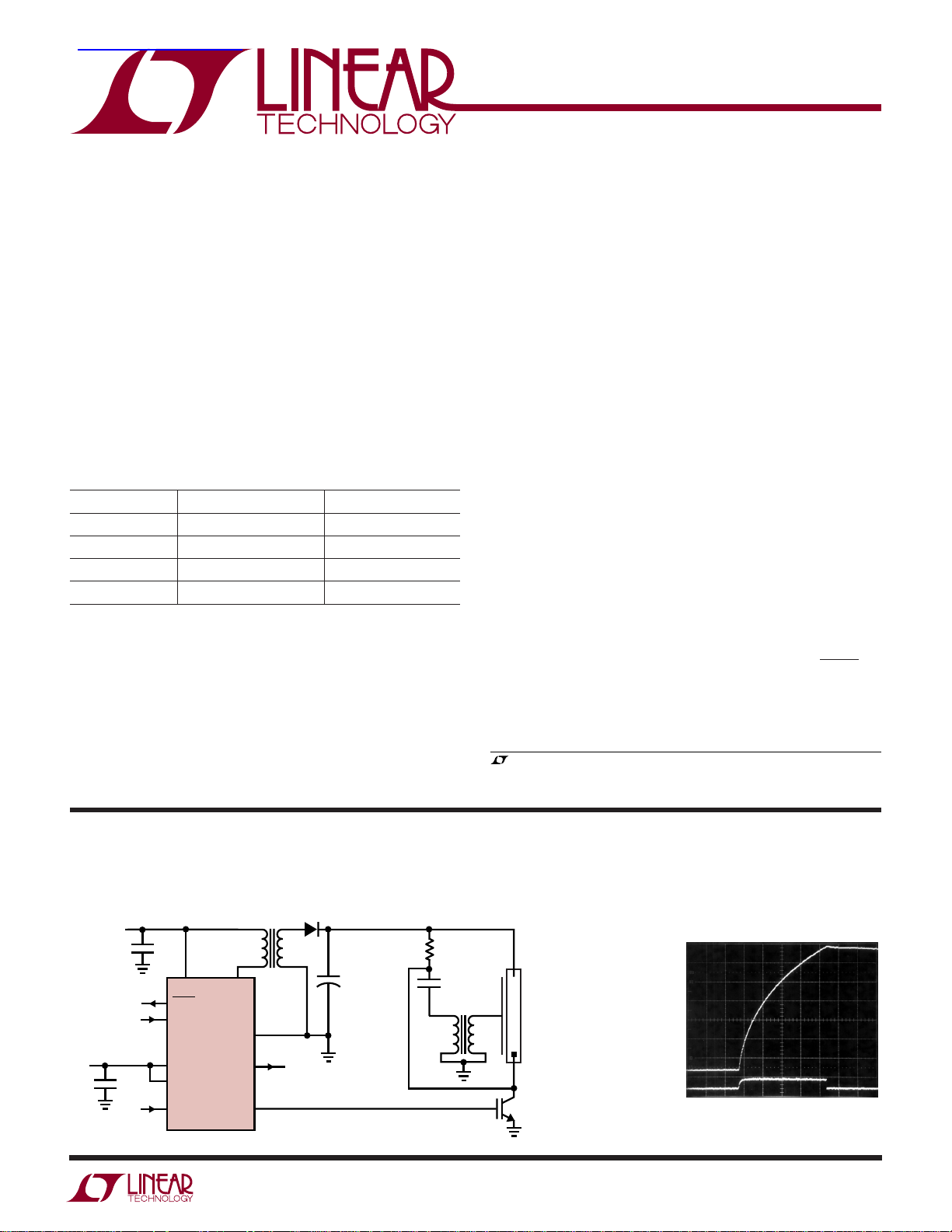
TYPICAL APPLICATIO
LT3485-0 Photoflash Charger Uses High Efficiency 3mm Tall Transformers
DANGER HIGH VOLTAGE – OPERATION BY HIGH VOLTAGE TRAINED PERSONNEL ONLY
V
BAT
2 AA OR
1 TO 2 Li-Ion
V
CC
5V
0.22µF
4.7µF
V
BAT
DONE
CHARGE
LT3485-0
V
IN
IGBTPWR
IGBTIN
SW
GND
V
MONT
IGBTOUT
1
2
1:10.2
•
•
4
5
TO
MICRO
320V
150µF
PHOTOFLASH
CAPACITOR
1M
2.2µF
600V
TRIGGER
1
2
3
3485 TA01
T
A
FLASHLAMP
C
IGBT
V
OUT
50V/DIV
AVERAGE
INPUT CURRENT
0.5A/DIV
LT3485-0 Charging Waveform
VIN = 3.6V
= 100µF
C
OUT
1s/DIV
3485 TA02
34850123f
1

LT3485-0/LT3485-1/
LT3485-2/LT3485-3
WW
W
U
ABSOLUTE AXI U RATI GS
(Note 1)
VIN Voltage .............................................................. 10V
Voltage ............................................................ 10V
V
BAT
SW Voltage ................................................... –1V to 50V
SW Pin Negative Current ...................................... –0.5A
CHARGE Voltage...................................................... 10V
IGBTIN Voltage ........................................................ 10V
IGBTOUT Voltage ..................................................... 10V
DONE Voltage .......................................................... 10V
IGBTPWR Voltage.................................................... 10V
V
Voltage ......................................................... 10V
MONT
Current into DONE Pin ...............................0.2mA/–1mA
Maximum Junction Temperature .......................... 125°C
Operating Temperature Range (Note 2) ... –40°C to 85°C
Storage Temperature Range ..................–65°C to 125°C
UUW
PACKAGE/ORDER I FOR ATIO
TOP VIEW
CHARGE
EXPOSED PAD (11) IS GND, MUST BE SOLDERED TO PCB
1
V
2
BAT
V
IN
SW
SW
10-LEAD (3mm ´ 3mm) PLASTIC DFN
T
11
3
4
5
DD PACKAGE
= 125°C θJA = 43°C/W
JMAX
ORDER PART NUMBER
LT3485EDD-0
LT3485EDD-1
LT3485EDD-2
LT3485EDD-3
Order Options Tape and Reel: Add #TR
Lead Free: Add #PBF Lead Free Tape and Reel: Add #TRPBF
Lead Free Part Marking: http://www.linear.com/leadfree/
Consult LTC Marketing for parts specified with wider operating temperature ranges.
10
V
MONT
DONE
9
IGBTPWR
8
7
IGBTIN
6
IGBTOUT
DD PART MARKING
LBRH
LBVN
LBVP
LBTK
ELECTRICAL CHARACTERISTICS
temperature range, otherwise specifications are at TA = 25°C. VIN = V
PARAMETER CONDITIONS MIN TYP MAX UNITS
Quiescent Current Not Switching 5 8 mA
VIN Voltage Range
V
Voltage Range
BAT
Switch Current Limit LT3485-3 1.6 1.7 1.8 A
Switch V
CESAT
V
Comparator Trip Voltage Measured as VSW – V
OUT
V
Comparator Overdrive 300ns Pulse Width 200 400 mV
OUT
DCM Comparator Trip Voltage Measured as VSW – V
CHARGE Pin Current V
The ● denotes the specifications which apply over the full operating
= V
BAT
= 0V 0 1 µA
V
CHARGE
LT3485-0 1.1 1.2 1.3 A
LT3485-2 0.75 0.85 0.95 A
LT3485-1 0.45 0.55 0.65 A
LT3485-3, I
LT3485-0, I
LT3485-2, I
LT3485-1, I
CHARGE
V
CHARGE
= 1.5A 310 400 mV
SW
= 1A 210 300 mV
SW
= 700mA 170 225 mV
SW
= 400mA 100 175 mV
SW
IN
IN
= 3V 65 100 µA
= 0V 0 0.1 µA
= 3V, unless otherwise noted.
CHARGE
●
●
●
●
2.5 10 V
1.7 10 V
31 31.5 32 V
10 45 120 mV
2
34850123f
LT3485-0/LT3485-1/
LT3485-2/LT3485-3
ELECTRICAL CHARACTERISTICS
temperature range, otherwise specifications are at T
PARAMETER CONDITIONS MIN TYP MAX UNITS
Switch Leakage Current V
CHARGE Input Voltage High
CHARGE Input Voltage Low
Minimum Charge Pin Low Time High→Low→High 20 µs
DONE Output Signal High 100kΩ from VIN to DONE 3 V
DONE Output Signal Low 33µA into DONE Pin 140 200 mV
DONE Leakage Current V
IGBT Input Voltage High
IGBT Input Voltage Low
IGBT Output Rise Time C
IGBT Output Fall Time C
V
Monitor Accuracy SW – V
OUT
Monitor Output Current 200 µA
Note 1: Absolute Maximum Ratings are those values beyond which the life
of a device may be impaired.
The ● denotes the specifications which apply over the full operating
= 25°C. VIN = V
A
= V
= 5V, in Shutdown
IN
SW
= 3V, DONE NPN Off 20 100 nA
DONE
= 4000pF, IGBTPWR = 5V, 10%→90% 200 270 320 ns
OUT
= 4000pF, IGBTPWR = 5V, 90%→10% 130 180 230 ns
OUT
= 20V 610 625 640 mV
BAT
SW – V
= 30V 920 940 960 mV
BAT
= V
BAT
Note 2: The LTC3485E-X is guaranteed to meet performance specifications
from 0°C to 70°C. Specifications over the –40°C to 85°C operating
temperature range are assured by design, characterization and correlation
with statistical process controls.
= 3V, unless otherwise noted.
CHARGE
●
●
●
●
●
0.01 1 µA
1V
0.3 V
1.5 V
0.3 V
34850123f
3
LT3485-0/LT3485-1/
V
OUT
50V/DIV
0.5s/DIVV
IN
= 3.6V
C
OUT
= 50µF
3485 G03
AVERAGE
INPUT
CURRENT
0.5A/DIV
V
OUT
(V)
0
INPUT CURRENT (mA)
400
500
600
150 250
3485 G06
300
200
50 100
200 300
100
0
2.5V
3.6V
4.2V
V
OUT
(V)
0
0
INPUT CURRENT (mA)
100
300
400
500
200
900
3485 G09
200
100
50
250 300
150
600
700
800
2.5V
3.6V
4.2V
LT3485-2/LT3485-3
UW
TYPICAL PERFOR A CE CHARACTERISTICS
curves use the circuit of Figure 9, LT3485-2 use the circuit of Figure 10 and LT3485-3 use the circuit of Figure 11 unless otherwise noted.
LT3485-0 curves use the circuit of Figure 8, LT3485-1
V
OUT
50V/DIV
AVERAGE
INPUT
CURRENT
1A/DIV
V
OUT
50V/DIV
AVERAGE
INPUT
CURRENT
1A/DIV
LT3485-0 Charging Waveform
C
= 3.6V
IN
OUT
= 50µF
0.5s/DIVV
3485 G01
AVERAGE
CURRENT
LT3485-1 Charging Waveform
V
OUT
50V/DIV
INPUT
0.5A/DIV
C
= 3.6V
IN
OUT
= 50µF
LT3485-3 Charging Waveform Charge Time
6
LT3485-1
5
4
3
2
CHARGE TIME (SECONDS)
1
0
LT3485-0
2
3
C
= 3.6V
IN
OUT
= 50µF
0.5s/DIVV
3485 G04
0.5s/DIVV
C
OUT
LT3485-2
LT3485-3
456
VIN (V)
LT3485-2 Charging Waveform
3485 G02
LT3485-0 Input Current
= 50µF
78
1635 G05
4
LT3485-1 Input Current LT3485-2 Input Current LT3485-3 Input Current
250
200
150
100
INPUT CURRENT (mA)
50
0
050
100
200
150
V
(V)
OUT
250
2.5V
3.6V
4.2V
300
3485 G07
400
300
200
INPUT CURRENT (mA)
100
0
0
50 100 150 200
2.5V
3.6V
4.2V
V
(V)
OUT
250 300
3485 G08
34850123f
LT3485-0/LT3485-1/
V
OUT
(V)
50
40
EFFICIENCY (%)
50
60
70
80
90
100
150 200 250
3485 G12
300
2.5V
3.6V
4.2V
TEMPERATURE (°C)
–40 –20
0
CURRENT LIMIT (mA)
800
2000
0
40
60
3485 G18
400
1600
1200
20
80
100
LT3485-3
LT3485-0
LT3485-2
LT3485-1
LT3485-2/LT3485-3
UW
TYPICAL PERFOR A CE CHARACTERISTICS
curves use the circuit of Figure 9, LT3485-2 use the circuit of Figure 10 and LT3485-3 use the circuit of Figure 11 unless otherwise noted.
LT3485-0 Efficiency LT3485-1 Efficiency LT3485-2 Efficiency
90
90
LT3485-0 curves use the circuit of Figure 8, LT3485-1
80
70
60
EFFICIENCY (%)
50
40
50
100
LT3485-3 Efficiency
90
80
70
60
EFFICIENCY (%)
50
40
50
100
150 200 250
V
(V)
OUT
150 200 250
V
(V)
OUT
2.5V
3.6V
4.2V
300
3485 G10
2.5V
3.6V
4.2V
300
3485 G13
80
70
60
EFFICIENCY (%)
50
40
50
150 200 250
100
V
LT3485-0 Output Voltage
322
321
320
(V)
OUT
V
319
318
317
2
456
3
VIN (V)
OUT
(V)
2.5V
3.6V
4.2V
300
3485 G11
–40°C
25°C
85°C
78
3485 G14
LT3485-1 Output Voltage
322
321
320
(V)
OUT
V
319
318
317
2
456
3
–40°C
25°C
85°C
78
VIN (V)
3485 G15
328
327
326
(V)
325
OUT
V
324
323
322
LT3485-2 Output Voltage LT3485 Switch Current Limits
–40°C
25°C
85°C
2
456
3
VIN (V)
78
3485 G16
LT3485-3 Output Voltage
322
321
320
(V)
OUT
V
319
318
317
2
456
3
VIN (V)
–40°C
25°C
85°C
78
3485 G17
34850123f
5
LT3485-0/LT3485-1/
LT3485-2/LT3485-3
UW
TYPICAL PERFOR A CE CHARACTERISTICS
curves use the circuit of Figure 9, LT3485-2 use the circuit of Figure 10 and LT3485-3 use the circuit of Figure 11 unless otherwise noted.
LT3485-0 curves use the circuit of Figure 8, LT3485-1
LT3485-0 Switching Waveform
V
SW
10V/DIV
I
PRI
1A/DIV
V
= 3.6V
IN
OUT
= 100V
1µs/DIVV
LT3485-3 Switching Waveform
V
SW
10V/DIV
I
PRI
2A/DIV
VIN = 3.6V
= 100V
V
OUT
1µs/DIV
LT3485-2 Switching Waveform
V
SW
10V/DIV
I
PRI
1A/DIV
V
= 3.6V
IN
OUT
= 300V
1µs/DIVV
3485 G19
3485 G22
3485 G25
LT3485-1 Switching Waveform
V
SW
10V/DIV
I
PRI
1A/DIV
= 100V
V
OUT
1µs/DIVVIN = 3.6V
LT3485-0 Switching Waveform
V
SW
10V/DIV
I
PRI
1A/DIV
V
= 3.6V
IN
OUT
= 300V
1µs/DIVV
LT3485-3 Switching Waveform
V
SW
10V/DIV
I
PRI
2A/DIV
VIN = 3.6V
= 300V
V
OUT
1µs/DIV
3485 G26
3485 G20
3485 G23
LT3485-2 Switching Waveform
V
SW
10V/DIV
I
PRI
1A/DIV
V
= 3.6V
IN
OUT
= 100V
1µs/DIVV
LT3485-1 Switching Waveform
V
SW
10V/DIV
I
PRI
1A/DIV
V
= 3.6V
IN
OUT
= 300V
1µs/DIVV
LT3485-0/LT3485-1/LT3485-2/
LT3485-3 Switch Breakdown
Voltage
10
SW PIN IS RESISTIVE UNTIL BREAKDOWN
VOLTAGE DUE TO INTEGRATED
9
RESISTORS. THIS DOES NOT INCREASE
8
QUIESCENT CURRENT OF PART
7
6
5
4
3
SWITCH CURRENT (mA)
2
1
0
0 102030405060708090100
SWITCH VOLTAGE (V)
T = 25°C
T = –40°C
VIN = V
T = 85°C
CHARGE
3485 G21
3485 G24
= 5V
3485 G27
6
34850123f

LT3485-0/LT3485-1/
LT3485-2/LT3485-3
U
UU
PI FU CTIO S
CHARGE (Pin 1): Charge Pin. A low (<0.3V) to high (>1V)
transition on this pin puts the part into power delivery
mode. Once the target voltage is reached, the part will stop
charging the output. Toggle this pin to start charging
again. Bringing the pin low (<0.3V) will terminate the
power delivery and put the part in shutdown.
V
(Pin 2): Battery Supply Pin. Must be locally bypassed
BAT
with a good quality ceramic capacitor. Battery supply
must be 1.7V or higher.
V
(Pin 3): Input Supply Pin. Must be locally bypassed
IN
with a good quality ceramic capacitor. Input supply must
be 2.5V or higher.
SW (Pins 4, 5): Switch Pin. This is the collector of the
internal NPN power switch. Minimize the metal trace area
connected to this pin to minimize EMI. Tie one side of the
primary of the transformer to this pin. The target output
voltage is set by the turns ratio of the transformer.
Choose Turns Ratio N by the following equation:
IGBTOUT (Pin 6): Output Drive for IGBT Gate. Connect
this pin to the gate of the IGBT.
IGBTIN (Pin 7): Logic Input Pin for IGBT Drive. When this
pin is driven higher than 1.5V, the IGBT output pin goes
high. When the pin is below 0.3V, the output is low.
IGBTPWR (Pin 8): Input Supply Pin. Must be locally
bypassed with a good quality ceramic capacitor. Input
supply must be 0.1V higher than the turn-on voltage for
the IGBT.
DONE (Pin 9): Open NPN Collector Indication Pin. When
target output voltage is reached, NPN turns on. This pin
needs a pull-up resistor or current source.
V
(Pin 10): Supplies a voltage proportional to the
MONT
output voltage where 1V is the end of charge voltage. Only
valid while the part is charging.
Exposed Pad (Pin 11): Ground. Tie directly to local
ground plane.
N
=
where V
V
+ 2
OUT
31 5.
is the desired output voltage.
OUT
34850123f
7

LT3485-0/LT3485-1/
LT3485-2/LT3485-3
UU
W
FU CTIO AL BLOCK DIAGRA
TO BATTERY
CHIP
POWER
ENABLE
COMPARATOR
LT3485-3: R
LT3485-0: R
LT3485-2: R
LT3485-1: R
C1
R3
4k
+
A2
OUT
–
SENSE
SENSE
SENSE
SENSE
V
CHARGE
TO V
IGBTON
TO V
IN
C2
DONE
9 10 3 2
Q3
ONE-
1
SHOT
IGBT
DRIVER
8
IN
7
DRIVER
POWER
IGBT
6
TO GATE OF IGBT
QQ
SR
20Ω
20k
V
MONT
SAMPLE
AND HOLD
R1
2.5k
1.25V
REFERENCE
ONESHOT
= 0.010Ω
= 0.015Ω
= 0.022Ω
= 0.030Ω
D1
T1
PRIMARY
R2
60k
R4
Q2
120k
ONE-
SHOT
DCM
COMPARATOR
+
A3
SW
4, 5
SECONDARY
V
OUT
C
OUT
PHOTOFLASH
CAPACITOR
–
+
60mV
–
DRIVER
S
RQ
Q1
+
R
–
+
20mV
SENSE
–
GND
11
3485 F01
A1
8
Figure 1
34850123f

OPERATIO
LT3485-0/LT3485-1/
LT3485-2/LT3485-3
U
The LT3485-0/LT3485-1/LT3485-2/LT3485-3 are designed
to charge photoflash capacitors quickly and efficiently. The
operation of the part can be best understood by referring
to Figure 1. When the CHARGE pin is first driven high, a one
shot sets both SR latches in the correct state. The power
NPN device, Q1, turns on and current begins ramping up
in the primary of transformer T1. Comparator A1 monitors
the switch current and when the peak current reaches 2A
(LT3485-3), 1.4A (LT3485-0), 1A (LT3485-2) or 0.7A
(LT3485-1), Q1 is turned off. Since T1 is utilized as a flyback
transformer, the flyback pulse on the SW pin will cause the
output of A3 to be high. The voltage on the SW pin needs
to be at least 60mV higher than V
for this to happen.
BAT
During this phase, current is delivered to the photoflash
capacitor via the secondary and diode D1. As the secondary current decreases to zero, the SW pin voltage will begin
to collapse. When the SW pin voltage drops to 60mV above
V
or lower, the output of A3 (DCM Comparator) will go
BAT
low. This fires a one shot which turns Q1 back on. This cycle
will continue to deliver power to the output.
Output voltage detection is accomplished via R2, R1, Q2,
and comparator A2 (V
Comparator). Resistors R1 and
OUT
R2 are sized so that when the SW voltage is 31.5V above
V
, the output of A2 goes high which resets the master
BAT
latch. This disables Q1 and halts power delivery. NPN
transistor Q3 is turned on pulling the DONE pin low,
indicating that the part has finished charging. Power
delivery can only be restarted by toggling the CHARGE pin.
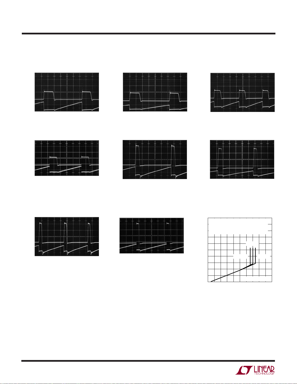
The CHARGE pin gives full control of the part to the user.
The charging can be halted at any time by bringing the
CHARGE pin low. Only when the final output voltage is
reached will the DONE pin go low. Figure 2 shows these
various modes in action. When CHARGE is first brought
high, charging commences. When CHARGE is brought
low during charging, the part goes into shutdown and
no longer rises. When CHARGE is brought high
V
OUT
again, charging resumes. When the target V
voltage is
OUT
reached, the DONE pin goes low and charging stops.
Finally the CHARGE pin is brought low again so the part
enters shutdown and the DONE pin goes high.
Both V
and VIN have undervoltage lockout (UVLO).
BAT
When one of these pins goes below its UVLO voltage, the
DONE pin goes low. With an insufficient bypass capacitor
on V
or VIN, the ripple on the pin is likely to activate
BAT
UVLO and terminate the charge. The applications circuits
in the data sheet suggest values adequate for most
applications.
The LT3485 V
pin functions as an output to a
MONT
microcontroller to communicate the progress of the charge.
The V
pin starts to function at about 0.2V, which
MONT
corresponds to 64V with a turns ratio of 10.2. When the
V
pin is at 1V, the DONE pin goes low and the
MONT
charging terminates. The pin’s output is only valid when
the part is charging.
The LT3485 also integrates an IGBT drive. The IGBTPWR
pin supplies the power. The IGBT output goes high when
IGBTIN goes high and conversely goes low when IGBTIN
goes low. While IGBTIN is low, the IGBT drive draws no
quiescent current from IGBTPWR.
V
OUT
100V/DIV
V
DONE
5V/DIV
V
CHARGE
5V/DIV
LT3485-2
= 3.6V
V
IN
= 50µF
C
OUT
Figure 2. Halting the Charging Cycle with the CHARGE Pin
1s/DIV
3485 F02
34850123f
9

LT3485-0/LT3485-1/
L
V
NI
PRI
OUT
PK
≥
−
••
•
200 10
9
LT3485-2/LT3485-3
U
WUU
APPLICATIO S I FOR ATIO
Choosing the Right Device
(LT3485-0/LT3485-1/LT3485-2/LT3485-3)
The only difference between the four versions of the
LT3485 is the peak current level. For the fastest possible
charge time, use the LT3485-3. The LT3485-1 has the
lowest peak current capability, and is designed for
applications that need a more limited drain on the
batteries. Due to the lower peak current, the LT3485-1 can
use a physically smaller transformer. The LT3485-0 and
LT3485-2 have a current limit in between that of the
LT3485-3 and the LT3485-1.
Transformer Design
The flyback transformer is a key element for any
LT3485-0/LT3485-1/LT3485-2/LT3485-3 design. It must
be designed carefully and checked that it does not cause
excessive current or voltage on any pin of the part. The
main parameters that need to be designed are shown in
Table 1.
The first transformer parameter that needs to be set is the
turns ratio N. The LT3485-0/LT3485-1/LT3485-2/LT34853 accomplish output voltage detection by monitoring the
flyback waveform on the SW pin. When the SW voltage
reaches 31.5V higher than the V
halt power delivery. Thus, the choice of N sets the target
output voltage as it changes the amplitude of the reflected
voltage from the output to the SW pin. Choose N according to the following equation:
V
+ 2
OUT
N
=
31 5.
voltage, the part will
BAT
where V
is the desired output voltage. The number 2
OUT
in the numerator is used to include the effect of the voltage
drop across the output diode(s).
Thus for a 320V output, N should be 322/31.5 or 10.2. For
a 300V output, choose N equal to 302/31.5 or 9.6.
The next parameter that needs to be set is the primary
inductance, L
. Choose L
PRI
according to the following
PRI
formula:
where V
former turns ratio. I
is the desired output voltage. N is the trans-
OUT
is 1.4 (LT3485-0), 0.7 (LT3485-1),
PK
1 (LT3485-2) and 2 (LT3485-3).
L
needs to be equal or larger than this value to ensure
PRI
that the LT3485-0/LT3485-1/LT3485-2/LT3485-3 has adequate time to respond to the flyback waveform.
All other parameters need to meet or exceed the recommended limits as shown in Table 1. A particularly important parameter is the leakage inductance, L
. When the
LEAK
power switch of the LT3485-0/LT3485-1/LT3485-2/
LT3485-3 turns off, the leakage inductance on the primary of the transformer causes a voltage spike to occur
on the SW pin. The height of this spike must not exceed
40V, even though the absolute maximum rating of the SW
Pin is 50V. The 50V absolute maximum rating is a DC
blocking voltage specification, which assumes that the
current in the power NPN is zero. Figure 3 shows the SW
voltage waveform for the circuit of Figure 8 (LT3485-0).
Table 1. Recommended Transformer Parameters
TYPICAL RANGE TYPICAL RANGE TYPICAL RANGE TYPICAL RANGE
PARAMETER NAME LT3485-0 LT3485-1 LT3485-2 LT3485-3 UNITS
L
PRI
L
LEAK
N Secondary: Primary Turns Ratio 8 to 12 8 to 12 8 to 12 8 to 12
V
ISO
I
SAT
R
PRI
R
SEC
10
Primary Inductance >5 >10 >7 >3.5 µH
Primary Leakage Inductance 100 to 300 200 to 500 200 to 500 100 to 300 nH
Secondary to Primary Isolation Voltage >500 >500 >500 >500 V
Primary Saturation Current >1.6 >0.8 >1.0 >2 A
Primary Winding Resistance <300 <500 <400 <200 mΩ
Secondary Winding Resistance <40 <80 <60 <30 Ω
34850123f

LT3485-0/LT3485-1/
VVNV
PK R OUT IN−
=+(• )
LT3485-2/LT3485-3
U
WUU
APPLICATIO S I FOR ATIO
Note that the absolute maximum rating of the SW pin is
not ex
ceeded. Make sure to check the SW voltage waveform with V
worst case condition for SW voltage. Figure 4 shows the
various limits on the SW voltage during switch turn off.
It is important not to minimize the leakage inductance to
a very low level. Although this would result in a very low
leakage spike on the SW pin, the parasitic capacitance of
the transformer would become large. This will adversely
affect the charge time of the photoflash circuit.
Linear Technology has worked with several leading magnetic component manufacturers to produce pre-designed
flyback transformers for use with the LT3485-0/LT34851/LT3485-2/LT3485-3. Table 2 shows the details of several of these transformers.
10A/DIV
near the target output voltage, as this is the
OUT
I
PRI
1A/DIV
2
V
SW
Capacitor Selection
For the input bypass capacitors, high quality X5R or X7R
types should be used. Make sure the voltage capability of
the part is adequate.
Output Diode Selection
The rectifying diode(s) should be low capacitance type
with sufficient reverse voltage and forward current ratings. The peak reverse voltage that the diode(s) will see is
approximately:
“B”
“A”
V
SW
MUST BE
LESS THAN 50V
MUST BE
LESS THAN 40V
0V
= 5V
V
IN
= 320V
V
OUT
Figure 3. LT3485 SW Voltage Waveform
Table 2. Pre-Designed Transformers – Typical Specifications Unless Otherwise Noted
FOR USE WITH NAME (W × L × H) mm (µH) (nH) N (mΩ)(Ω) VENDOR
LT3485-0/LT3485-2 SBL-5.6-1 5.6 × 8.5 × 4.0 10 200 Max 10.2 103 26 Kijima Musen
LT3485-1 SBL-5.6S-1 5.6 × 8.5 × 3.0 24 400 Max 10.2 305 55 Hong Kong Office
LT3485-0 LDT565630T-001 5.8 × 5.8 × 3.0 6 200 Max 10.4 100 Max 10 Max TDK
LT3485-1 LDT565630T-002 5.8 × 5.8 × 3.0 14.5 500 Max 10.2 240 Max 16.5 Max Chicago Sales Office
LT3485-2 LDT565630T-003 5.8 × 5.8 × 3.0 10.5 550 Max 10.2 210 Max 14 Max (847) 803-6100 (ph)
LT3485-3 LDT565630T-041 5.8 × 5.8 × 3.0 4.7 150 Max 10.4 90 Max 6.4 Max www.components.tdk.com
LT3485-0/LT3485-1 T-15-089 6.4 × 7.7 × 4.0 12 400 Max 10.2 211 Max 27 Max Tokyo Coil Engineering
LT3485-1 T-15-083 8.0 × 8.9 × 2.0 20 500 Max 10.2 675 Max 35 Max Japan Office
LT3485-3 T-17-109A 6.5 × 7.9 × 4.0 5.9 300 Max 10.2 78 Max 18.61 Max 0426-56-6262 (ph)
100ns/DIV
TRANSFORMER SIZE L
3485 F03
PRI LPRI-LEAKAGE
Figure 4. New Transformer Design Check (Not to Scale)
R
PRI
R
SEC
kijimahk@netvigator.com (email)
3485 F04
852-2489-8266 (ph)
www.tokyo-coil.co.jp
34850123f
11

LT3485-0/LT3485-1/
LT3485-2/LT3485-3
U
WUU
APPLICATIO S I FOR ATIO
The peak current of the diode is simply:
I=
PK-SEC
I=
PK-SEC
I=
PK-SEC
I=
PK-SEC
F
or the circuit of Figure 8 with V
and I
PK-SEC
is recommended for most LT3485-0/LT3485-1/LT34852/LT3485-3 applications. Another option is to use the
BAV23S dual silicon diodes. Table 3 shows the various
diodes and relevant specifications. Use the appropriate
number of diodes to achieve the necessary reverse breakdown voltage.
2
LT3485-3
()
N
1.4
LT3485-0
(
))
N
1
LT3485-2
()
N
0.7
LT3485-
()
11
N
of 5V, V
BAT
PK-R
is 371V
is 137mA. The GSD2004S dual silicon diode
V
IN = 5V
V
OUT = 320V
IGBT Drive
The IGBT is a high current switch for the 100A+ current
through the photoflash lamp. To create a redeye effect or
to adjust the light output, the lamp current needs to be
stopped, or quenched, with an IGBT before discharging
the photoflash capacitor fully. The IGBT device also controls the 4kV trigger pulse required to ionize the xenon gas
in the photoflash lamp. Figure 5 is a schematic of a fully
functional photoflash application with the LT3485 serving
as the IGBT drive. An IGBT drive charges the gate capacitance to start the flash. The IGBT drive does not need to
pull-up the gate fast because of the inherently slow nature
of the IGBT. A rise time of 2µs is sufficient to charge the
gate of the IGBT and create a trigger pulse. With slower
rise times, the trigger circuitry will not have a fast enough
edge to create the required 4kV pulse. The fall time of the
IGBT drive is critical to the safe operation of the IGBT. The
IGBT gate is a network of resistors and capacitors, as
shown in Figure 6. When the gate terminal is pulled low,
Table 3. Recommended Output Diodes
PART (V) (mA) (pF) VENDOR
GSD2004S 2x300 225 5 Vishay
(Dual Diode) (402) 563-6866
BAV23S 2x250 225 5 Philips Semiconductor
(Dual Diode) (800) 234-7381
MMBD3004S 2x350 225 5 Diodes Inc
(Dual Diode) (816) 251-8800
MAX REVERSE VOLTAGE MAX FORWARD CONTINUOUS CURRENT CAPACITANCE
V
BAT
2 AA OR
1 TO 2 Li-Ion
V
CC
5V
0.22µF
4.7µF
DONE
CHARGE
V
IGBTPWR
IGBTIN
V
BAT
IN
LT3485-0
IGBTOUT
V
SW
GND
MONT
1
2
1:10.2
•
•
4
5
TO
MICRO
320V
150µF
PHOTOFLASH
CAPACITOR
1M
2.2µF
600V
TRIGGER
1
2
3
T
3485 F05
www.vishay.com
www.philips.com
www.diodes.com
A
FLASHLAMP
C
IGBT
12
Figure 5. Complete Xenon Circuit
34850123f

LT3485-0/LT3485-1/
LT3485-2/LT3485-3
U
WUU
APPLICATIO S I FOR ATIO
GATE
3485 F06
EMITTER
Figure 6. IGBT Gate
the capacitance closest to the terminal goes low but the
capacitance further from the terminal remains high. This
causes a small portion of the device to handle the full 100A
of current, which quickly destroys the device. The pull
down circuitry needs to pull down slower than the internal
RC time constant in the gate of the IGBT. This is easily
accomplished with a resistor in series with the IGBT drive,
which is integrated into the LT3485.
The LT3485’s integrated drive circuit is independent of the
charging function. The IGBT section draws its power from
the IGBTPWR pin. The rise and fall times are measured
using a 4000pF output capacitor. The typical 10% to 90%
rise time is 270ns. The drive pulls high to IGBTPWR. The
typical 90% to 10% fall time is 180ns. The drive pulls
down to 300mV. The IGBT driver pulls a peak of 150mA
when driving an IGBT and 2mA of quiescent current. In the
low state, the IGBT’s quiescent current is less than 0.1µA.
Table 4 is a list of recommended IGBT devices for strobe
applications. These three devices are all packaged in
8-lead TSSOP packages.
V
Monitor
OUT
The voltage output monitor is a new feature to monitor the
progress of capacitor charging with a microcontroller.
The monitor uses the flyback waveform to output a
voltage proportional to the output of the flyback converter.
The output monitor voltage range for the pin is 0V to 1V.
The 1V output corresponds with the charge cycle terminating and the DONE pin going low. The voltage output
monitor is only functional when the circuit is charging
(DONE and CHARGE are high.)
Table 4. Recommended IGBTs
DRIVE BREAKDOWN COLLECTOR
VOLTAGE VOLTAGE CURRENT
PART (V) (V) (PULSED) (A) VENDOR
CY25BAH-8F 2.5 400 150 Renesas
CY25BAJ-8F 4 400 150 (408) 382-7500
www.renesas.com
GT8G133 4 400 150 Toshiba Semiconductor
(949) 623-2900
www.semicon.toshiba.co.jp/eng/
34850123f
13

LT3485-0/LT3485-1/
LT3485-2/LT3485-3
U
WUU
APPLICATIO S I FOR ATIO
Board Layout
The high voltage operation of the LT3485-0/LT3485-1/
LT3485-2/LT3485-3 demands careful attention to board
layout. You will not get advertised performance with
careless layout. Figure 7 shows the recommended component placement. Keep the area for the high voltage end
of the secondary as small as possible. Also note the larger
than minimum spacing for all high voltage nodes in order
CHARGE
C2 C3
•
C
OUT
PHOTOFLASH
CAPACITOR
V
IN
+
SECONDARY PRIMARY
T1
•
to meet breakdown voltage requirements for the circuit
board.
It is imperative to keep the electrical path formed
by C1, the primary of T1, and the LT3485-0/LT3485-1/
LT3485-2/LT3485-3 as short as possible.
If this path is
haphazardly made long, it will effectively increase the
leakage inductance of T1, which may result in an overvoltage condition on the SW pin.
1 10
3
5
C1
V
MONT
92
811
74
6
3485 F07
R1
DONE
IGBTPWR
IGBTIN
IGBTOUT
D1
(DUAL DIODE)
V
BAT
Figure 7. Suggested Layout: Keep Electrical Path Formed by C1,
Transformer Primary and LT3485-0/LT3485-1/LT3485-2/LT3485-3 Short
14
34850123f

TYPICAL APPLICATIO S
1.8V TO 8V
V
IN
2.5V TO 8V
U
T1
D1
TO MICRO
TO GATE OF IGBT
SW
GND
V
MONT
= 10µH, N = 10.2
PRI
1:10.2
3485 F08
V
BAT
C1
4.7µF
R1
V
BAT
100k
DONE
CHARGE
C2
0.22µF
C1: 4.7µF, X5R OR X7R, 10V
C2: 0.22µF, X5R or X7R, 10V
T1: KIJIMA MUSEN PART# SBL-5.6-1, L
D1: DIODES INC MMBD3004S DUAL DIODE CONNECTED IN SERIES
R1: PULL UP RESISTOR NEEDED IF DONE PIN USED
DONE
CHARGE
LT3485-0
V
IN
IGBTPWR
IGBTIN
IGBTOUT
LT3485-0/LT3485-1/
LT3485-2/LT3485-3
320V
C
OUT
PHOTOFLASH
CAPACITOR
Figure 8. LT3485-0 Photoflash Charger Uses High Efficiency 4mm Tall Transformer
T1
D1
TO MICRO
TO GATE OF IGBT
320V
C
OUT
PHOTOFLASH
CAPACITOR
V
2.5V TO 8V
V
SW
GND
MONT
PRI
1:10.2
3485 F09
= 24µH, N = 10.2
V
BAT
1.8V TO 8V
DONE
CHARGE
IN
C2
0.22µF
C1: 4.7µF, X5R OR X7R, 10V
C2: 0.22µF, X5R or X7R, 10V
T1: KIJIMA MUSEN PART# SBL-5.6S-1, L
D1: DIODES INC MMBD3004S DUAL DIODE CONNECTED IN SERIES
R1: PULL UP RESISTOR NEEDED IF DONE PIN USED
C1
4.7µF
R1
100k
V
BAT
DONE
CHARGE
LT3485-1
V
IN
IGBTPWR
IGBTIN
IGBTOUT
Figure 9. LT3485-1 Photoflash Charger Uses High Efficiency 3mm Tall Transformer
34850123f
15

LT3485-0/LT3485-1/
LT3485-2/LT3485-3
U
TYPICAL APPLICATIO S
1.8V TO 8V
CHARGE
V
IN
2.5V TO 8V
C1: 4.7µF, X5R OR X7R, 10V
C2: 0.22µF, X5R or X7R, 10V
T1: KIJIMA MUSEN PART# SBL-5.6-1, L
D1: DIODES INC MMBD3004S DUAL DIODE CONNECTED IN SERIES
R1: PULL UP RESISTOR NEEDED IF DONE PIN USED
V
DONE
BAT
C2
0.22µF
C1
4.7µF
R1
100k
V
BAT
DONE
CHARGE
LT3485-2
V
IN
IGBTPWR
IGBTIN
SW
GND
VMONT
IGBTOUT
= 10µH, N = 10.2
PRI
T1
1:10.2
TO MICRO
TO GATE OF IGBT
3485 F10
D1
320V
C
OUT
PHOTOFLASH
CAPACITOR
Figure 10. LT3485-2 Photoflash Charger Uses High Efficiency 4mm Tall Transformer
T1
D1
TO MICRO
TO GATE OF IGBT
320V
C
OUT
PHOTOFLASH
CAPACITOR
V
2.5V TO 8V
V
1:10.2
SW
GND
MONT
3485 F11
V
BAT
1.8V TO 8V
DONE
CHARGE
IN
C2
0.22µF
C1: 4.7µF, X5R OR X7R, 10V
C2: 0.22µF, X5R or X7R, 10V
T1: TDK LDT565630T-041, L
D1: DIODES INC MMBD3004S DUAL DIODE CONNECTED IN SERIES
R1: PULL UP RESISTOR NEEDED IF DONE PIN USED
C1
4.7µF
R1
100k
V
BAT
DONE
CHARGE
LT3485-3
V
IN
IGBTPWR
IGBTIN
= 4.7µH, N = 10.4
PRI
IGBTOUT
Figure 11. LT3485-3 Photoflash Charger Uses High Efficiency 3mm Tall Transformer
16
34850123f

TYPICAL APPLICATIO S
V
IN
2.5V TO 8V
U
T1
D1
TO MICRO
TO GATE OF IGBT
V
MONT
1:10.2
SW
GND
3485 F12
V
BAT
1.8V TO 8V
DONE
CHARGE
C2
0.22µF
C1: 4.7µF, X5R OR X7R, 10V
C2: 0.22µF, X5R or X7R, 10V
T1: TDK LDT565630T-001, L
D1: DIODES INC MMBD3004S DUAL DIODE CONNECTED IN SERIES
R1: PULL UP RESISTOR NEEDED IF DONE PIN USED
C1
4.7µF
V
BAT
DONE
CHARGE
LT3485-0
V
IN
IGBTPWR
IGBTIN
= 6µH, N = 10.4
PRI
IGBTOUT
LT3485-0/LT3485-1/
LT3485-2/LT3485-3
320V
C
OUT
PHOTOFLASH
CAPACITOR
Figure 12. LT3485-0 Photoflash Circuit Uses Tiny 3mm Tall Transformer
6
5
4
3
2
CHARGE TIME (SECONDS)
1
0
2
LT3485-1
LT3485-0
3
456
LT3485-2
LT3485-3
VIN (V)
C
= 50µF
OUT
78
3485 F13
Figure 13. Charge Time with TDK Transformers (Figures 11, 12, 13, 14 and 15)
34850123f
17

LT3485-0/LT3485-1/
LT3485-2/LT3485-3
U
TYPICAL APPLICATIO S
V
IN
2.5V TO 8V
T1
V
BAT
1.8V TO 8V
DONE
CHARGE
C2
0.22µF
C1: 4.7µF, X5R OR X7R, 10V
C2: 0.22µF, X5R or X7R, 10V
T1: TDK LDT565630T-002, L
D1: DIODES INC MMBD3004S DUAL DIODE CONNECTED IN SERIES
R1: PULL UP RESISTOR NEEDED IF DONE PIN USED
C1
4.7µF
V
BAT
DONE
CHARGE
LT3485-1
V
IN
IGBTPWR
IGBTOUT
IGBTIN
= 14.5µH, N = 10.2
PRI
1:10.2
SW
GND
VMONT
D1
TO MICRO
TO GATE OF IGBT
3485 F14
320V
C
OUT
PHOTOFLASH
CAPACITOR
Figure 14. LT3485-1 Photoflash Circuit Uses Tiny 3mm Tall Transformer
T1
D1
TO MICRO
TO GATE OF IGBT
3485 F15
320V
C
OUT
PHOTOFLASH
CAPACITOR
V
2.5V TO 8V
V
BAT
1.8V TO 8V
DONE
CHARGE
IN
C2
0.22µF
C1: 4.7µF, X5R OR X7R, 10V
C2: 0.22µF, X5R or X7R, 10V
T1: TDK LDT565630T-003, L
D1: DIODES INC MMBD3004S DUAL DIODE CONNECTED IN SERIES
R1: PULL UP RESISTOR NEEDED IF DONE PIN USED
C1
4.7µF
V
BAT
DONE
CHARGE
LT3485-2
V
IN
IGBTPWR
IGBTIN
= 10µH, N = 10.2
PRI
IGBTOUT
1:10.2
SW
GND
VMONT
Figure 15. LT3485-2 Photoflash Circuit Uses Tiny 3mm Tall Transformer
18
34850123f

PACKAGE DESCRIPTIO
LT3485-0/LT3485-1/
LT3485-2/LT3485-3
U
DD Package
10-Lead Plastic DFN (3mm × 3mm)
(Reference LTC DWG # 05-08-1699)
0.675 ±0.05
3.50 ±0.05
1.65 ±0.05
(2 SIDES)2.15 ±0.05
PACKAGE
OUTLINE
0.25 ± 0.05
RECOMMENDED SOLDER PAD PITCH AND DIMENSIONS
PIN 1
TOP MARK
(SEE NOTE 6)
0.200 REF
NOTE:
1. DRAWING TO BE MADE A JEDEC PACKAGE OUTLINE M0-229 VARIATION OF (WEED-2).
CHECK THE LTC WEBSITE DATA SHEET FOR CURRENT STATUS OF VARIATION ASSIGNMENT
2. DRAWING NOT TO SCALE
3. ALL DIMENSIONS ARE IN MILLIMETERS
4. DIMENSIONS OF EXPOSED PAD ON BOTTOM OF PACKAGE DO NOT INCLUDE
MOLD FLASH. MOLD FLASH, IF PRESENT, SHALL NOT EXCEED 0.15mm ON ANY SIDE
5. EXPOSED PAD SHALL BE SOLDER PLATED
6. SHADED AREA IS ONLY A REFERENCE FOR PIN 1 LOCATION ON THE
TOP AND BOTTOM OF PACKAGE
0.50
BSC
2.38 ±0.05
(2 SIDES)
3.00 ±0.10
(4 SIDES)
0.75 ±0.05
1.65 ± 0.10
(2 SIDES)
0.00 – 0.05
R = 0.115
TYP
2.38 ±0.10
(2 SIDES)
BOTTOM VIEW—EXPOSED PAD
106
15
0.50 BSC
0.38 ± 0.10
0.25 ± 0.05
(DD10) DFN 1103
Information furnished by Linear Technology Corporation is believed to be accurate and reliable.
However, no responsibility is assumed for its use. Linear Technology Corporation makes no representation that the interconnection of its circuits as described herein will not infringe on existing patent rights.
34850123f
19

LT3485-0/LT3485-1/
LT3485-2/LT3485-3
RELATED PARTS
PART NUMBER DESCRIPTION COMMENTS
LTC3407 Dual 600mA (I
Converter I
LT3420/LT3420-1 1.4A/1A, Photoflash Capacitor Chargers with Charges 220µF to 320V in 3.7 seconds from 5V,
Automatic Top-Off V
LTC3425 5A ISW, 8MHz, Multi-Phase Synchronous Step-Up DC/DC 95% Efficiency, VIN: 0.5V to 4.5V, V
Converter I
LTC3440 600mA/1A (I
Converter I
LT3468/LT3468-1/ Photoflash Capacitors in ThinSOT™ Charges 110µF to 320V in 4.6 Seconds from 3.6V,
LT3468-2 V
LT3472 Dual ±34V, 1.2MHz Boost (350mA)/Inverting (400mA) Integrated Schottkys, VIN: 2.2V to 16V, V
DC/DC Converter for CCD Bias I
LT3463/LT3463A Dual Boost (250mA)/Inverting (250mA/400mA) Integrated Schottkys, VIN: 2.3V to 15V, V
DC/DC Converter for CCD Bias I
LT3484-0/LT3484-1/ Photoflash Capacitor Chargers Charges 110µF to 320V in 4.6 Seconds from 3.6V,
LT3484-2 V
ThinSOT is a trademark of Linear Technology Corporation.
), 1.5MHz, Synchronous Step-Down DC/DC 96% Efficiency, VIN: 2.5V to 5.5V, V
OUT
), Synchronous Buck-Boost DC/DC 95% Efficiency, VIN: 2.5V to 5.5V, V
OUT
<1µA, MS10E
SD
: 2.2V to 16V, IQ = 90µA, ISD < 1µA, MS10
IN
< 1µA, QFN-32
SD
= 25µA, ISD < 1µA, MS-10 DFN-12
Q
: 2.5V to 16V, IQ = 5mA, ISD < 1µA, ThinSOT
IN
= 2.5mA, ISD < 1µA, DFN
Q
= 40µA, ISD < 1µA, DFN
Q
: 2.5V to 16V, V
IN
2mm × 3mm DFN
: 1.8V to 16V, IQ = 5mA, ISD < 1µA,
BAT
= 0.6V, IQ = 40µA,
OUT(MIN)
= 5.25V, IQ = 12µA,
OUT(MIN)
= 2.5V to 5.5V,
OUT(MIN)
OUT(MAX)
OUT(MAX)
= ±34V,
= ±40V,
20
Linear Technology Corporation
1630 McCarthy Blvd., Milpitas, CA 95035-7417
(408) 432-1900 ● FAX: (408) 434-0507 ● www.linear.com
34850123f
LT/LWI/TP 0805 500 • PRINTED IN USA
© LINEAR TECHNOLOGY CORPORATION 2005
 Loading...