

查询LT1617-1供应商
FEATURES
■
Internal 40V Schottky Diode
■
One Resistor Feedback (Other Resistor Inside)
■
Internal 40V, 200mA Power Switch
■
Generates Regulated Negative Outputs to –38V
■
Low Quiescent Current:
40µA in Active Mode
<1µA in Shutdown Mode
■
Low V
■
Wide Input Range: 2.5V to 16V
■
Uses Small Surface Mount Components
■
Output Short-Circuit Protected
■
Available in a 6-Lead SOT-23 Package
Switch: 200mV at 150mA
CESAT
U
APPLICATIO S
■
LCD Bias
■
Handheld Computers
■
Battery Backup
■
Digital Cameras
■
OLED Bias
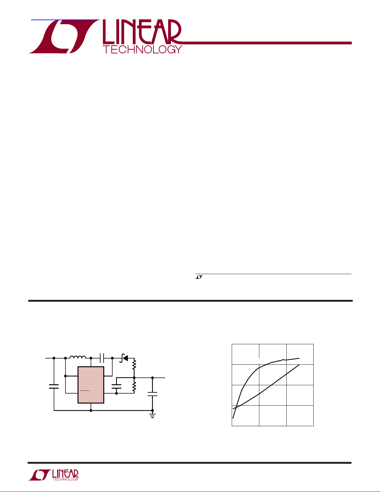
LT3483
Inverting Micropower
DC/DC Converter with
Schottky in ThinSOT Package
U
DESCRIPTIO
The LT®3483 is a micropower inverting DC/DC converter
with integrated Schottky and one resistor feedback. The
small package size, high level of integration and use of tiny
surface mount components yield a solution size as small
as 40mm
40µA at no load, which further reduces to 0.1µA in
shutdown. A current limited, fixed off-time control scheme
conserves operating current, resulting in high efficiency
over a broad range of load current. A precisely trimmed
10µA feedback current enables one resistor feedback and
virtually eliminates feedback loading of the output. The
40V switch enables voltage outputs up to –38V to be
generated without the use of costly transformers. The
LT3483’s low 300ns off-time permits the use of tiny low
profile inductors and capacitors to minimize footprint and
cost in space-conscious portable applications.
The LT3483 is available in the low profile (1mm) SOT-23
(ThinSOTTM) package.
, LTC and LT are registered trademarks of Linear Technology Corporation.
ThinSOT is a trademark of Linear Technology Corporation.
Patent pending.
2
. The device features a quiescent current of only
TYPICAL APPLICATIO
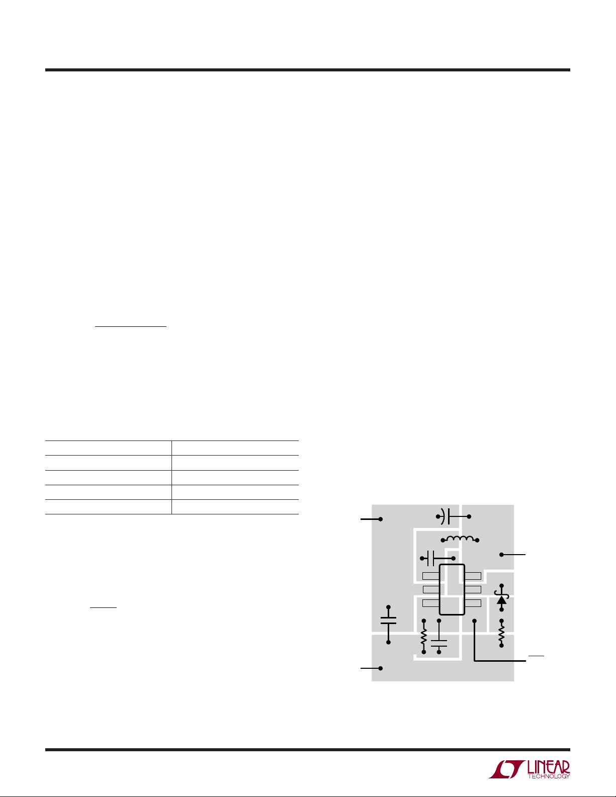
3.6V to –8V DC/DC Converter
V
IN
LT3483
SHDN
0.22µF
SW
D
FB
GND
V
3.6V
4.7µF
IN
10µH
U
10Ω
806k5pF
2.2µF
3483 TA01a
V
OUT
–8V
25mA
Efficiency and Power Loss
75
= 3.6V
V
IN
70
65
EFFICIENCY (%)
60
55
0.1
EFFICIENCY
POWER
LOSS
110
LOAD CURRENT (mA)
3483 TA01b
1000
100
POWER LOSS (mW)
10
1
0.1
100
3483f
1
LT3483
WWWU
ABSOLUTE AXI U RATI GS
(Note 1)
VIN Voltage ............................................................. 16V
SW Voltage ............................................................. 40V
D Voltage .............................................................. –40V
FB Voltage ............................................................. 2.5V
SHDN Voltage ......................................................... 16V
Operating Ambient Temperature Range
(Note 2) .................................................. – 40°C to 85°C
Junction Temperature.......................................... 125°C
Storage Temperature Range ................ –65°C to 150°C
PACKAGE/ORDER I FOR ATIO
TOP VIEW
SW 1
GND 2
FB 3
S6 PACKAGE
6-LEAD PLASTIC TSOT-23
T
= 125°C, θJA = 256°C/W IN FREE AIR
JMAX
= 120°C/W ON BOARD OVER GROUND PLANE
θ
JA
6 V
5 D
4 SHDN
UU
W
ORDER PART
NUMBER
IN
LT3483ES6
S6 PART MARKING
LTBKX
Lead Temperature (Soldering, 10 sec)................. 300°C
Consult LTC Marketing for parts specified with wider operating temperature ranges.
ELECTRICAL CHARACTERISTICS
The ● denotes specifications which apply over the full operating temperature range, otherwise specifications are TA = 25°C.
VIN = 3.6V, V
PARAMETER CONDITIONS MIN TYP MAX UNITS
VIN Operating Range 2.5 16 V
VIN Undervoltage Lockout 2 2.4 V
FB Comparator Trip Voltage to GND (VFB) FB Falling ● 0512 mV
FB Output Current (Note 3) FB = VFB – 5mV ● –10.15 –10 –9.75 µA
FB Comparator Hysteresis FB Rising 10 mV
Quiescent Current in Shutdown V
Quiescent Current (Not Switching) FB = –0.05V 40 50 µA
IFB Line Regulation 2.5V ≤ VIN ≤ 16V 0.07 %/V
Switch Off-Time 300 ns
Switch Current Limit 170 200 230 mA
Switch V
CESAT
Switch Leakage Current SW = 40V 1 µA
Rectifier Leakage Current D = – 40V 4 µA
Rectifier Forward Drop ID = 150mA to GND 0.64 V
SHDN Input Low Voltage 0.4 V
SHDN Input High Voltage 1.5 V
SHDN Pin Current 610 µA
= 3.6V unless otherwise specified.
SHDN
= GND 1 µA
SHDN
ISW = 150mA to GND 200 mV
Note 1: Absolute Maximum Ratings are those values beyond which the life
of a device may be impaired.
Note 2: The LTC3483E is guaranteed to meet specifications from 0°C to
70°C. Specifications over the –40°C to 85°C operating temperature range
are assured by design, characterization and correlation with statistical
process controls.
2
Note 3: Current flows out of the pin.
3483f
UW
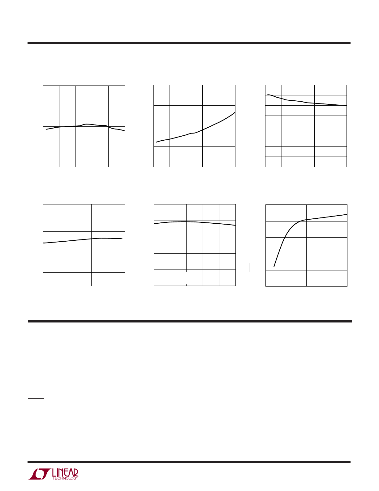
TYPICAL PERFOR A CE CHARACTERISTICS
LT3483
CURRENT (µA)
V
FB
10.2
10.1
10.0
9.9
9.8
–50
VFB Current
–20
40
10
TEMPERATURE (°C)
70
100
3483 G01
VFB Voltage Switch Off Time
12
9
6
VOLTAGE (mV)
FB
V
3
0
–50
–20
10
TEMPERATURE (°C)
40
70
100
3483 G02
400
350
300
250
200
150
SWITCH OFF TIME (ns)
100
50
0
–50
–20 10 70
TEMPERATURE (°C)
Switch Current Limit Quiescent Current SHDN Pin Bias Current
230
220
210
200
190
SWITCH CURRENT LIMIT (mA)
180
170
–50
–20 10 40 70
TEMPERATURE (°C)
100
3483 G04
50
40
30
20
QUIESCENT CURRENT (µA)
10
0
–50
NOT SWITCHING
= –0.05V
V
FB
–20
TEMPERATURE (°C)
10
= 25°C
T
A
8
6
4
2
SHDN PIN BIAS CURRENT (µA)
40
70
10
100
3483 G05
0
0
4
SHDN PIN VOLTAGE (V)
40
8
12
100
3483 G03
16
3483 G06
U
UU
PI FU CTIO S
SW: Switch. Connect to external inductor L1 and positive
terminal of transfer capacitor.
GND: Ground.
FB: Feedback. Place resistor to negative output here. Set
resistor value R1 = V
SHDN: Shutdown. Connect to GND to turn device off.
Connect to supply to turn device on.
OUT
/10µA.
D: Anode Terminal of Integrated Schottky Diode. Connect to negative terminal of transfer capacitor and external inductor L2 (flyback configuration) or to cathode of
external Schottky diode (inverting charge pump
configuration).
VIN: Input Supply. Must be locally bypassed with 1µF or
greater.
3483f
3

LT3483
BLOCK DIAGRA
W
V
IN
6
V
1.250V
REFERENCE
125k
R1
V
OUT
FB
3
+
A3
300ns
DELAY
S
Q
RQ
–
IN
+
A1
–
GND
2
OPTIONAL CHARGE PUMP CONFIGURATION.
L1B REPLACED WITH:
D2
D
R2
V
OUT
••
C
FLY
1
SW D
Q1
0.1Ω 0.1Ω
20mV
L1BL1A
5
D1
25mV
V
OUT
C
OUT
+
A2
–
3483 BD
U
OPERATIO
The LT3483 uses a constant off-time control scheme to
provide high efficiency over a wide range of output currents. Operation can be best understood by referring to the
Block Diagram. When the voltage at the FB pin is approximately 0V, comparator A3 disables most of the internal circuitry. Output current is then provided by external capacitor
C
, which slowly discharges until the voltage at the FB
OUT
pin goes above the hysteresis point of A3. Typical hysteresis at the FB pin is 10mV. A3 then enables the internal
circuitry, turns on power switch Q1, and the currents in
external inductors L1A and L1B begin to ramp up. Once the
switch current reaches 200mA, comparator A1 resets the
latch, which turns off Q1 after about 80ns. Inductor current flows through the internal Schottky D1 to GND, charging the flying capacitor. Once the 300ns off-time has
elapsed, and internal diode current drops below 250mA
(as detected by comparator A2), Q1 turns on again and
ramps up to 200mA. This switching action continues until
the output capacitor charge is replenished (until the FB pin
decreases to 0V), then A3 turns off the internal circuitry
and the cycle repeats. The inverting charge pump topology
replaces L1B with the series combination D2 and R2.
4
3483f
WUUU
APPLICATIO S I FOR ATIO
LT3483
CHOOSING A REGULATOR TOPOLOGY
Inverting Charge Pump
The inverting charge pump regulator combines an inductor-based step-up with an inverting charge pump. This
configuration usually provides the best size, efficiency and
output ripple and is applicable where the magnitude of
V
is greater than VIN. Negative outputs to –38V can be
OUT
produced with the LT3483 in this configuration. For cases
where the magnitude of V
is less than or equal to VIN,
OUT
use a 2-inductor or transformer configuration such as the
inverting flyback.
In the inverting charge pump configuration, a resistor is
added in series with the Schottky diode between the
negative output and the D pin of the LT3483. The purpose
of this resistor is to smooth/reduce the current spike in the
flying capacitor when the switch turns on. A 10Ω resistor
works well for a Li
+
to –8V application, and the impact to
converter efficiency is less than 3%. The resistor values
recommended in the applications circuits also limit the
switch current during a short-circuit condition at the
output.
Inverting Flyback
The inverting flyback regulator, shown in the –5V application circuit, uses a coupled inductor and is an excellent
choice where the magnitude of the output is less than or
equal to the supply voltage. The inverting flyback also
performs well in a step-up/invert application, but it occupies more board space compared with the inverting charge
pump. Also, the maximum |V
| using the flyback is less
OUT
than can be obtained with the charge pump—it is reduced
from 38V by the magnitudes of VIN and ringing at the
switch node. Under a short-circuit condition at the output,
a proprietary technique limits the switch current and
prevents damage to the LT3483 even with supply voltage
as high as 16V. As an option, a 0.47µF capacitor may be
added between terminals D and SW of LT3483 to suppress
ringing at SW.
Inductor Selection
Several recommended inductors that work well with the
LT3483 are listed in Table 1, although there are many other
manufacturers and devices that can be used. Consult each
manufacturer for more detailed information and for their
entire selection of related parts. Many different sizes and
shapes are available. For inverting charge pump regulators with input and output voltages below 7V, a 4.7µH or
6.8µH inductor is usually the best choice. For flyback
regulators or for inverting charge pump regulators where
the input or output voltage is greater than 7V, a 10µH
inductor is usually the best choice. A larger value inductor
can be used to slightly increase the available output
current, but limit it to around twice the value recommended, as too large of an inductance will increase the
output voltage ripple without providing much additional
output current.
Table 1. Recommended Inductors
MAX
LIDCDCR HEIGHT
µ
PART (
LQH2MCN4R7M02L 4.7 300 0.84 0.95 Murata
LQH2MCN6R8M02L 6.8 255 1.0 www.murata.com
LQH2MCN100M02L 10 225 1.2
SDQ12 10 980 0.72 1.2 Cooper Electronics
Coupled 15 780 1.15 Tech
Inductor www.cooperet.com
744876 10 550 0.46 1.2 Würth Elektronik
Coupled www.we-online.com
Inductor
H) (mA) (Ω) (mm) MANUFACTURER
Capacitor Selection
The small size and low ESR of ceramic capacitors make
them ideal for LT3483 applications. Use of X5R and X7R
types is recommended because they retain their capacitance
over wider voltage and temperature ranges than other dielectric types. Always verify the proper voltage rating. Table
2 shows a list of several ceramic capacitor manufacturers.
Consult the manufacturers for more detailed information
on their entire selection of ceramic capacitors.
A 4.7µF ceramic bypass capacitor on the VIN pin is
recommended where the distance to the power supply or
battery could be more than a couple inches. Otherwise, a
1µF is adequate.
3483f
5
LT3483
WUUU
APPLICATIO S I FOR ATIO
A capacitor in parallel with feedback resistor R1 is recommended to reduce the output voltage ripple. Use a 5pF
capacitor for the inverting charge pump, and a 22pF value
for the inverting flyback or other dual inductor configurations. Output voltage ripple can be reduced to 20mV in some
cases using this capacitor in combination with an appropriately selected output capacitor.
The output capacitor is selected based on desired output
voltage ripple. For low output voltage ripple in the inverting
flyback configuration, use a 4.7µF to 10µF capacitor. The
inverting charge pump utilizes values ranging from 0.22µF
to 4.7µF. The following formula is useful to estimate the
output capacitor value needed:
2
LI
•
C
OUT
where I
=
–•
= 0.25A and ∆V
SW
SW
VV
∆
OUT OUT
OUT
= 30mV. The flying capacitor in the inverting charge pump configuration ranges
from 0.1µF to 0.47µF. Multiply the value predicted by the
above equation for C
by 1/10 to determine the value
OUT
needed for the flying capacitor.
Table 2. Recommended Ceramic Capacitor Manufacturers
MANUFACTURER URL
AVX www.avxcorp.com
Kemet www.kemet.com
Murata www.murata.com
Taiyo Yuden www.tyuden.com
Setting the Output Voltage
The output voltage is programmed using one feedback
resistor according to the following formula:
V
R
110=µ–
OUT
A
Inrush Current
When VIN is increased from ground to operating voltage,
an inrush current will flow through the input inductor and
integrated Schottky diode to charge the flying capacitor.
Conditions that increase inrush current include a larger,
more abrupt voltage step at VIN, a larger flying capacitor,
and an inductor with a low saturation current.
While the internal diode is designed to handle such events,
the inrush current should not be allowed to exceed 1.5A.
For circuits that use flying capacitors within the recommended range and have input voltages less than 5V,
inrush current remains low, posing no hazard to the
device. In cases where there are large steps at V
, inrush
IN
current should be measured to ensure operation within the
limits of the device.
Board Layout Considerations
As with all switching regulators, careful attention must be
given to the PCB board layout and component placement.
Proper layout of the high frequency switching path is
essential. The voltage signals of the SW and D pins have
sharp rising and falling edges. Minimize the length and
area of all traces connected to the SW and D pins. In
particular, it is desirable to minimize the trace length to
and from the flying capacitor, since current in this capacitor switches directions within a cycle. Always use a
ground plane under the switching regulator to minimize
interplane coupling.
Suggested Layout (SOT-23)
for Inverting Charge Pump
+
GND
V
OUT
C
OUT
C
IN
L1
C
FLY
1
2
3
R1
6
5
4
3483 AI01
V
IN
SHDN
6
3483f
TYPICAL APPLICATIO
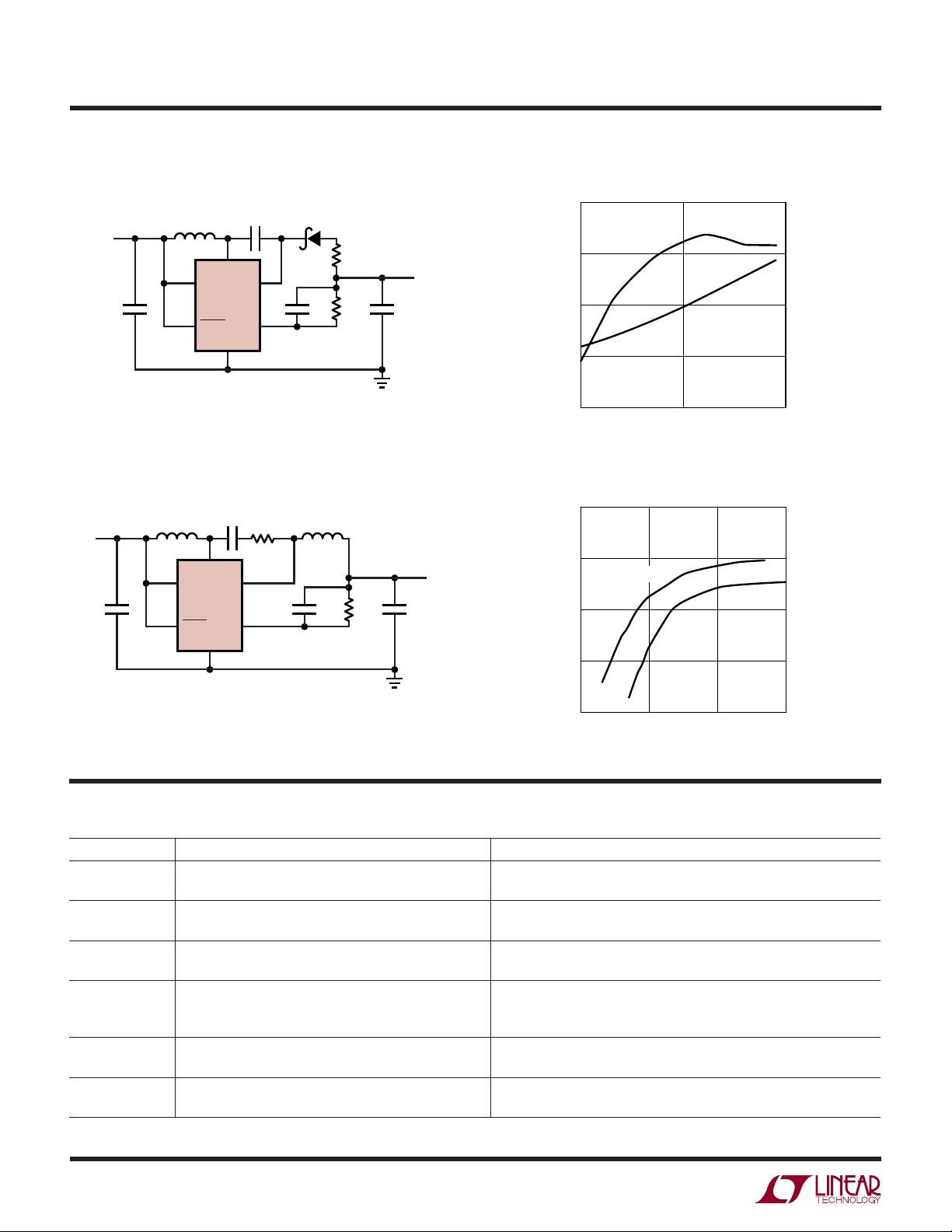
3.6V to –8V DC/DC Converter
Low Profile, Small Footprint
LT3483
U
SW
IN
LT3483
GND
C2
0.22µF
D
FB
D1
5pF
L1
V
IN
3.6V
C1
4.7µF
C1: MURATA GRM219R61A475KE34B
C2: TAIYO YUDEN LMK107BJ224
C3: MURATA GRM219R61C225KA88B
D1: PHILIPS PMEG2005EB
L1: MURATA LQH2MCN100K02L
10µH
V
SHDN
PACKAGE DESCRIPTIO
0.62
MAX
0.95
REF
10Ω
R1
806k
C3
2.2µF
3483 TA04a
V
OUT
–8V
25mA
U
S6 Package
6-Lead Plastic TSOT-23
(Reference LTC DWG # 05-08-1636)
V
OUT
20mV/DIV
I
SW
100mA/DIV
Switching Waveform
2µs/DIV
2.90 BSC
(NOTE 4)
3483 TA04b
3.85 MAX
2.62 REF
RECOMMENDED SOLDER PAD LAYOUT
PER IPC CALCULATOR
0.20 BSC
DATUM ‘A’
NOTE:
1. DIMENSIONS ARE IN MILLIMETERS
2. DRAWING NOT TO SCALE
3. DIMENSIONS ARE INCLUSIVE OF PLATING
1.22 REF
1.4 MIN
0.30 – 0.50 REF
2.80 BSC
0.09 – 0.20
(NOTE 3)
4. DIMENSIONS ARE EXCLUSIVE OF MOLD FLASH AND METAL BURR
5. MOLD FLASH SHALL NOT EXCEED 0.254mm
6. JEDEC PACKAGE REFERENCE IS MO-193
1.50 – 1.75
(NOTE 4)
PIN ONE ID
0.95 BSC
0.80 – 0.90
1.00 MAX
1.90 BSC
0.30 – 0.45
6 PLCS (NOTE 3)
0.01 – 0.10
S6 TSOT-23 0302
3483f
Information furnished by Linear Technology Corporation is believed to be accurate and reliable.
However, no responsibility is assumed for its use. Linear Technology Corporation makes no representation that the interconnection of its circuits as described herein will not infringe on existing patent rights.
7
LT3483
TYPICAL APPLICATIO S
U
3.6V to –22V DC/DC Converter
L1A
10µH
10µH
V
SHDN
V
IN
3.6V
C1
4.7µF
C1: TAIYO YUDEN LMK316BJ475MD
C2: TAIYO YUDEN TMK107BJ104 (X5R)
C3: TAIYO YUDEN TMK316BJ105MD
D1: PHILIPS PMEG3002AEB
L1: MURATA LQH2MCN100K02L
V
IN
C1
4.7µF
C1: TAIYO YUDEN EMK316BJ475ML
C2: TAIYO YUDEN JMK316BJ106ML
L1A, L1B: WURTH 744876100
SW
IN
LT3483
GND
C2
0.1µF
D
FB
D1
R
S
30Ω
R1
5pF
2.2M
L1
V
SHDN
–5V DC/DC Converter
1nF
10Ω
••
SW
D
IN
LT3483
FB
GND
L1B
10µH
22pF
511k
C3
1µF
3483 TA02a
C2
10µF
3483 TA03a
V
OUT
–22V
8mA
V
–5V
OUT
3.6V to –22V Converter Efficiency and Power Loss
75
70
65
EFFICIENCY (%)
60
55
0.1
EFFICIENCY
POWER
LOSS
1
LOAD CURRENT (mA)
3483 TA02b
1000
100
POWER LOSS (mW)
10
1
0.1
10
–5V Efficiency
75
70
65
EFFICIENCY (%)
60
55
0.1
VIN = 5V
= 12V
V
IN
110
LOAD CURRENT (mA)
100
3483 TA03b
RELATED PARTS
PART NUMBER DESCRIPTION COMMENTS
LT1617/LT1617-1 350mA/100mA (ISW) High Efficiency VIN: 1.2V to 15V, V
Micropower Inverting DC/DC Converter ThinSOT Package
LT1931/LT1931A 1A (ISW), 1.2MHz/2.2MHz, High Efficiency VIN: 2.6V to 16V, V
Micropower Inverting DC/DC Converter ThinSOT Package
LT1945 Dual Output, Boost/Inverter, 350mA (ISW), Constant VIN: 1.2V to 15V, V
Off-Time, High Efficiency Step-Up DC/DC Converter MS10 Package
LT3463 Dual Output, Boost/Inverter, 250mA (ISW), Constant VIN: 2.3V to 15V, V
Off-Time, High Efficiency Step-Up DC/DC Converter DFN Package
with Integrated Schottky Diodes
LT3464 85mA (ISW), High Efficiency Step-Up DC/DC Converter VIN: 2.3V to 10V, V
with Integrated Schottky and PNP Disconnect ThinSOT Package
LT3472 Boost (350mA) and Inverting (400mA) DC/DC Converter VIN: 2.3V to 15V, V
for CCD Bias with Integrated Schottkys DFN Package
Linear Technology Corporation
8
1630 McCarthy Blvd., Milpitas, CA 95035-7417
(408) 432-1900 ● FAX: (408) 434-0507
●
www.linear.com
= –34V, IQ = 20µA, ISD < 1µA
OUT(MAX)
= –34V, IQ = 5.8mA, ISD < 1µA
OUT(MAX)
= ±34V, IQ = 40µA, ISD < 1µA,
OUT(MAX)
= ±40V, IQ = 40µA, ISD < 1µA
OUT(MAX)
= 34V, IQ = 25µA, ISD < 1µA
OUT(MAX)
= ±40V, IQ = 2.8mA, ISD < 1µA
OUT(MAX)
© LINEAR TECHNOLOGY CORPORATION 2004
3483f
LT/TP 1004 1K • PRINTED IN THE USA
 Loading...