

FEATURES
■
True Color PWM™ Dimming Delivers Constant LED
Color with Up to 3000:1 Range
■
Wide Input Voltage Range: 2.8V to 36V
■
4.5A, 60mΩ, 42V Internal Switch
■
Drives LEDs in Boost, Buck-Boost or Buck Modes
■
Integrated Resistors for Inductor and LED Current
Sensing
■
Program LED Current:
100mA to 1050mA (LT3478-1)
(10mV to 105mV)/R
■
Program LED Current De-Rating vs Temperature
■
Separate Inductor Supply Input
■
Inrush Current Protection
■
Programmable Soft-Start
■
Fixed Frequency Operation from 200kHz to 2.25MHz
■
Open LED Protection (Programmable OVP)
■
Accurate Shutdown/UVLO Threshold with
SENSE
(LT3478)
Programmable Hysteresis
■
16-Pin Thermally Enhanced TSSOP Package
U
APPLICATIO S
LT3478/LT3478-1
4.5A Monolithic LED
Drivers with True Color
PWM Dimming
U
DESCRIPTIO
The LT®3478/LT3478-1 are 4.5A step-up DC/DC converters designed to drive LEDs with a constant current over
a wide programmable range. Series connection of the
LEDs provides identical LED currents for uniform brightness without the need for ballast resistors and expensive
factory calibration.
The LT3478-1 reduces external component count and cost
by integrating the LED current sense resistor. The LT3478
uses an external sense resistor to extend the maximum
programmable LED current beyond 1A and also to achieve
greater accuracy when programming low LED currents.
Operating frequency can be set with an external resistor
from 200kHz up to 2.25MHz. Unique circuitry allows a
PWM dimming range up to 3000:1 while maintaining
constant LED color. The LT3478/LT3478-1 are ideal for
high power LED driver applications such as automotive TFT
LCD backlights, courtesy lighting and heads-up displays.
One of two CTRL pins can be used to program maximum
LED current. The other CTRL pin can be used to program
a reduction in maximum LED current vs temperature to
maximize LED usage and improve reliability.
■
High Power LED Driver
■
Automotive Lighting
, LT, LTC and LTM are registered trademarks of Linear Technology Corporation.
All other trademarks are the property of their respective owners. Patents Pending.
U
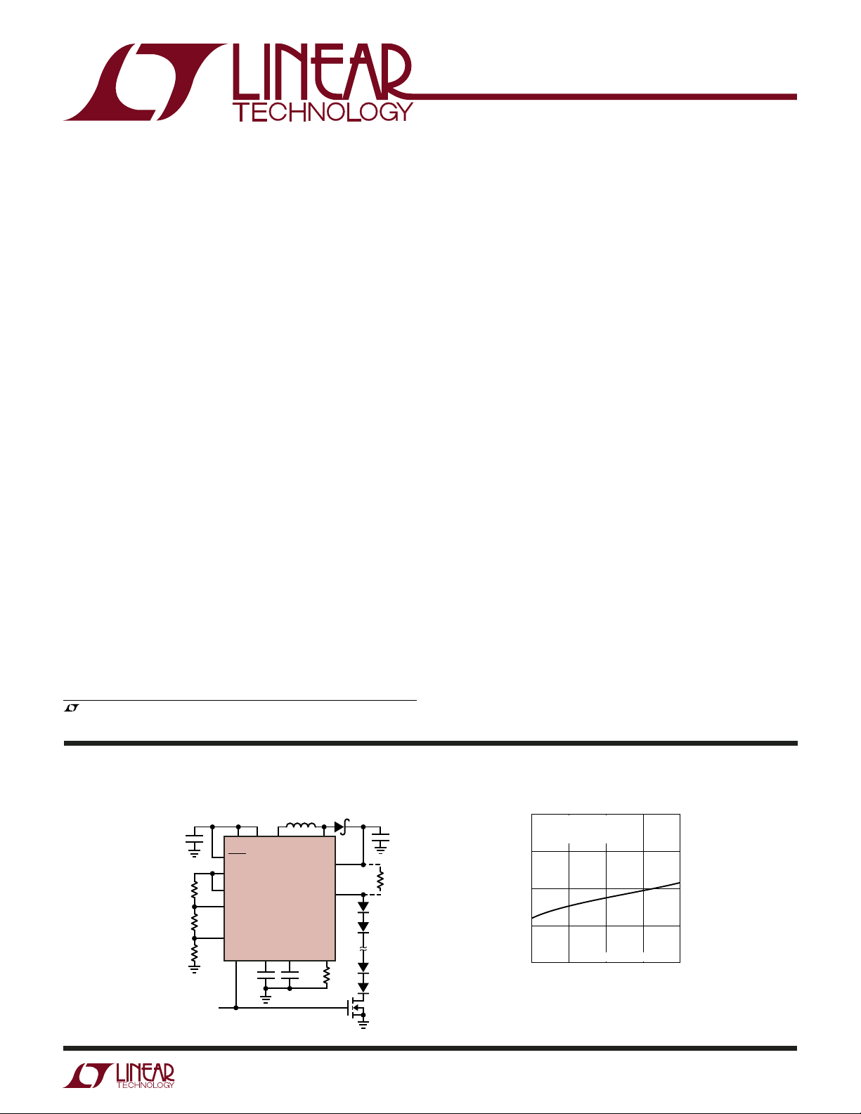
TYPICAL APPLICATIO
Automotive TFT LCD Backlight
LT3478-1
10µH
C
OUT
LED
R
T
0.1µF1µF
69.8k
4.7µF
45.3k
54.9k
130k
PWM DIMMING
CONTROL
8V TO 16V
V
IN
VINVSLSW
SHDN
V
REF
CTRL2
OVPSET
CTRL1
PWM SS V
10µF
0.1Ω
R
SENSE
(LT3478)
700mA
15W
6 LEDs
(WHITE)
3478 TA01
Additional features include inrush current protection,
programmable open LED protection and programmable
soft-start. Each part is available in a 16-pin thermally
enhanced TSSOP Package.
Effi ciency vs V
100
I
= 700mA
LED
= 500kHz
f
OSC
PWM DUTY CYCLE = 100%
95
90
EFFICIENCY (%)
85
80
8
6 LEDs LUXEON III (WHITE)
VIN (V)
IN
14 16
1210
3478 TA01b
34781f
1
LT3478/LT3478-1
WW
W
U
ABSOLUTE AXI U RATI GS
(Note 1)
SW ............................................................................42V
, LED ..................................................................42V
V
OUT
, VS, VL, ⎯S⎯H⎯D⎯N (Note 5) .......................................36V
V
IN
PWM .........................................................................15V
CTRL1, 2 .....................................................................6V
, VC, V
SS, R
T
Operating Junction Temperature Range
(Notes 2, 3, 4) .................................... –40°C to 125°C
Storage Temperature Range ................... –65°C to 150°C
Lead Temperature (Soldering, 10 Sec) .................. 300°C
, OVPSET ............................................2V
REF
UUW
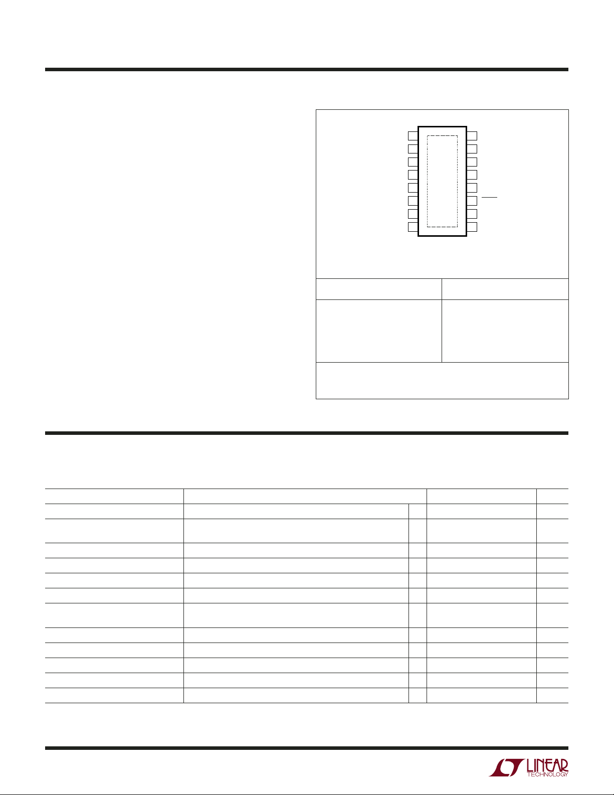
PACKAGE/ORDER I FOR ATIO
TOP VIEW
1
SW
2
SW
3
V
IN
4
V
S
L
V
OUT
LED
OVPSET
16-LEAD PLASTIC TSSOP
T
EXPOSED PAD (PIN 17) IS PGND, MUST BE SOLDERED TO PCB.
JMAX
17
5
6
7
8
FE PACKAGE
= 125°C, θJA = 35°C/W
ORDER PART NUMBER FE PART MARKING
LT3478EFE
LT3478EFE-1
LT3478IFE
LT3478IFE-1
Order Options Tape and Reel: Add #TR
Lead Free: Add #PBF Lead Free Tape and Reel: Add #TRPBF
Lead Free Part Marking: http://www.linear.com/leadfree/
Consult LTC Marketing for parts specifi ed with wider operating temperature ranges.
SS
16
R
15
T
PWM
14
CTRL2
13
CTRL1
12
SHDN
11
V
10
REF
V
9
C
3478FE
3478FE-1
3478FE
3478FE-1
●
The
ELECTRICAL CHARACTERISTICS
temperature range, otherwise specifi cations are at T
PWM = CTRL1, CTRL2 = 1.25V, V
PARAMETER CONDITIONS MIN TYP MAX UNITS
Minimum Operating Voltage (Rising)
Operational Input Voltage V
Quiescent Current VC = 0V (No Switching) 6.1 mA
V
IN
Shutdown Current
V
IN
⎯S⎯H⎯D⎯
N Pin Threshold (V
⎯S⎯H⎯D⎯
N Pin Threshold (V
⎯S⎯H⎯D⎯
N Pin Current
Voltage I(V
V
REF
Line Regulation I(V
V
REF
Load Regulation 0 < I(V
V
REF
Frequency: f
Frequency: f
200kHz RT = 200k 0.18 0.2 0.22 MHz
OSC
1MHz RT = 31.6k
OSC
) (Micropower)
SD_µp
) (Switching) 1.3 1.4 1.5 V
SD_UVLO
= open, VC = open, RT = 31.6k.
REF
S
VIN (Note 5)
⎯S⎯H⎯D⎯
N = 0V 3 6 µA
⎯S⎯H⎯D⎯
N = V
⎯S⎯H⎯D⎯
SD_UVLO
N = V
SD_UVLO
) = 0µA, VC = 0V
REF
) = 0µA, 2.7V < VIN < 36V 0.005 0.015 %/V
REF
) < 100µA (Max) 8 12 mV
REF
= 25°C. SW = open, VIN = VS = L = V
A
– 50mV
+ 50mV
denotes the specifi cations which apply over the full operating
= ⎯S⎯H⎯D⎯N = 2.7V, LED = open, SS = open,
OUT
●
2.8
2.8
●
0.1 0.4 0.7 V
810012 µA
●
1.213 1.240 1.263 V
●
0.88 1.12 MHz
2.4 2.8 V
36
36
µA
34781f
V
V
2

LT3478/LT3478-1
The
ELECTRICAL CHARACTERISTICS
temperature range, otherwise specifi cations are at T
PWM = CTRL1, CTRL2 = 1.25V, V
= open, VC = open, RT = 31.6k.
REF
= 25°C. SW = open, VIN = VS = L = V
A
●
denotes the specifi cations which apply over the full operating
= ⎯S⎯H⎯D⎯N = 2.7V, LED = open, SS = open,
OUT
PARAMETER CONDITIONS MIN TYP MAX UNITS
Frequency: f
Line Regulation f
Nominal R
Maximum Duty Cycle R
LED Current to V
LED Current to V
to Switch Current Gain 13 A/V
V
C
Source Current (Out of Pin) CTRL1 = 0.4V, VC = 1V 40 µA
V
C
Sink Current CTRL1 = 0V, VC = 1V 40 µA
V
C
Switching Threshold 0.65 V
V
C
High Level (VOH) CTRL1 = 0.4V 1.5 V
V
C
Low Level (VOL) CTRL1 = 0V 0.2 V
V
C
Inductor Current Limit 2.7V < V
Switch Current Limit
Switch V
Switch Leakage Current SW = 42V, V
Overvoltage Protection (OVP)
V
OUT
(Rising)
Full Scale LED Current (LT3478-1) CTRL1 = V
700mA LED Current (LT3478-1) CTRL1 = 700mV, Current Out of LED Pin
2.25MHz RT = 9.09k 2 2.25 2.6 MHz
OSC
OSC
Pin Voltage 0.64 V
T
Current Gain (Note 6) 770 µA/A
C
Voltage Gain (Note 6) 400 V/A
C
SAT ISW = 4.5A 270 mV
CE
RT = 31.6k, 2.7V < VIN < 36V 0.05 0.2 %/V
= 31.6k
T
R
= 200k
T
R
= 9.09k
T
< 36V
S
= 0V 1 µA
C
OVPSET = 1V
OVPSET = 0.3V
, Current Out of LED Pin 1010 1050 1090 mA
REF
●
80 88
97
73
●
4.5 6 6.8 A
●
4.5 6.3 7.5 A
41
12.3
●
655 700 730 mA
%
%
%
350mA LED Current (LT3478-1) CTRL1 = 350mV, Current Out of LED Pin 325 350 375 mA
100mA LED Current (LT3478-1) CTRL1 = 100mV, Current Out of LED Pin 70 100 130 mA
Full Scale LED Current V
CTRL1 = 700mV, V
CTRL1 = 350mV, V
CTRL1 = 100mV, V
SENSE
SENSE
SENSE
(LT3478) CTRL1 = V
SENSE
(LT3478) CTRL1 = 700mV, V
(LT3478) CTRL1 = 350mV, V
(LT3478) CTRL1 = 100mV, V
CTRL1, 2 Input Currents CTRL1 = 100mV, CTRL2 = 1.25V or
REF
, V
SENSE
SENSE
SENSE
SENSE
= V
= V
= V
= V
VOUT
VOUT
VOUT
VOUT
– V
LED
– V
– V
– V
LED
LED
LED
101 105 109 mV
●
67 70.5 74 mV
33 35.5 38 mV
71013 mV
40 nA
CTRL2 = 100mV, CTRL1 = 1.25V (Current Out of Pin)
OVPSET Input Current OVPSET = 1V, V
= 41V (Current Out of Pin) 200 nA
OUT
PWM Switching Threshold 0.8 1 1.2 V
Pin Current in PWM Mode VC = 1V, PWM = 0 1 50 nA
V
C
OUT Pin Current in PWM Mode PWM = 0 1 100 nA
SS Low Level (V
)I
OL
SS Reset Threshold V
SS High Level (V
)V
OH
Soft-Start (SS) Pin Charge Current SS = 1V, Current Out of Pin, V
Soft-Start (SS) Pin Discharge Current SS = 0.5V, V
= 20µA 0.15 V
(SS)
= 0V 0.25 V
C
= 0V 1.5 V
C
= 0V 12 µA
C
= 0V 350 µA
C
V
V
34781f
3
LT3478/LT3478-1
ELECTRICAL CHARACTERISTICS
Note 1: Stresses beyond those listed under Absolute Maximum Ratings
may cause permanent damage to the device. Exposure to any Absolute
Maximum Rating condition for extended periods may affect device
reliability and lifetime.
Note 2: The LT3478EFE/LT3478EFE-1 are guaranteed to meet performance
specifi cations from 0°C to 125°C junction temperature. Specifi cations over
the –40°C to 125°C operating junction temperature range are assured by
design, characterization and correlation with statistical process controls.
The LT3478IFE/LT3478IFE-1 are guaranteed over the full –40°C to 125°C
operating junction temperature range.
Note 3: This IC includes over-temperature protection that is intended
temperature will exceed 125°C when over-temperature protection is active.
Continuous operation above the specifi ed maximum operating junction
temperature may impair device reliability.
Note 4: For maximum operating ambient temperature, see the “Thermal
Calculations” section in the Applications Information section.
Note 5: The maximum operational voltage for V
effi ciency considerations. Power switch base current is delivered from V
and should therefore be driven from the lowest available power supply in
the system. See “Thermal Calculations” in the Applications Information
section.
Note 6: For LT3478, parameter scales • (R
to protect the device during momentary overload conditions. Junction
UW
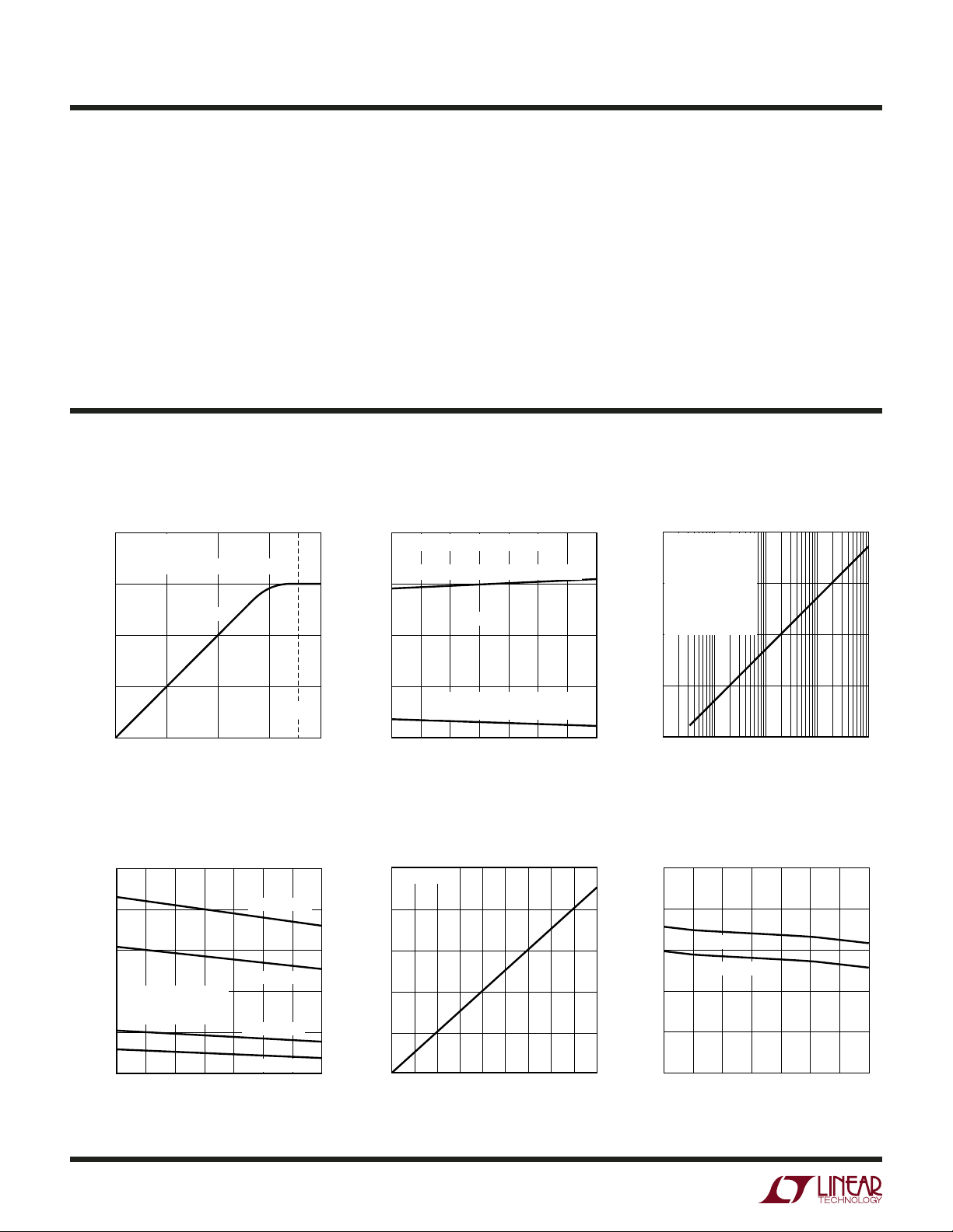
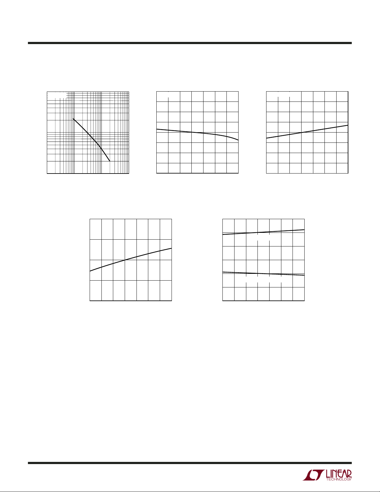
TYPICAL PERFOR A CE CHARACTERISTICS
LED Current vs CTRL1 LED Current vs Temperature
1400
TA = 25°C
CTRL2 = V
REF
(FOR LT3478 SCALE BY 0.1Ω/R
1050
700
LT3478-1
SENSE
)
1400
(FOR LT3478 SCALE BY 0.1Ω/R
I
= 1050mA, CTRL1 = CTRL2 = V
1050
LED
700
SENSE
LT3478-1
is limited by thermal and
SENSE
IN
/0.1Ω).
IN
LED Current vs PWM Duty Cycle
Wide PWM Dimming Range
(3000:1)
1000
)
REF
TA = 25°C
= VS = 12V
V
IN
6 LEDS AT 500mA
PWM FREQ = 100Hz
100
CTRL1 = 0.5V
CTRL2 = V
F
= 1.6MHz
OSC
L = 2.2µH
10
REF
LED CURRENT (mA)
350
0
0
0.35 0.70 1.05
CTRL1 (V)
CTRL1 Pin Current vs
Temperature
50
40
30
20
CTRL2 = V
CTRL1 AND CTRL2 PINS
INTERCHANGEABLE
10
CTRL1 PIN CURRENT X (–1) (nA)
0
–50
REF
–25 0 25
JUNCTION TEMPERATURE (°C)
V
REF
1.40
3478 G01
CTRL1 = 0.1V
CTRL1 = 0.35V
CTRL1 = 0.7V
CTRL1 = 0.9V
50 75 100 125
3478 G04
LED CURRENT (mA)
350
0
–50
I
LED
CTRL2 = V
–25 0 25
JUNCTION TEMPERATURE (°C)
Switch V
Current
240
TA = 25°C
210
180
(SAT) (mV)
CE
120
SWITCH V
60
0
0.5 1.5 3.0 3.5 4.0
1.0 2.0 2.5 4.5
0.0
= 100mA, CTRL1 = 100mV,
REF
50 75 100 125
(SAT) vs Switch
CE
SWITCH CURRENT (A)
3478 G02
3478 G05
LED CURRENT (mA)
1
0
0.01 1 10 100
0.1
PWM DUTY CYCLE (%)
Switch and Inductor Peak Current
Limits vs Temperature
7.0
6.5
6.0
5.5
CURRENT LIMIT (A)
5.0
4.5
–50
SWITCH
INDUCTOR
–25 0 25
JUNCTION TEMPERATURE (°C)
50 75 100 125
3478 G03
3478 G06
4
34781f
UW
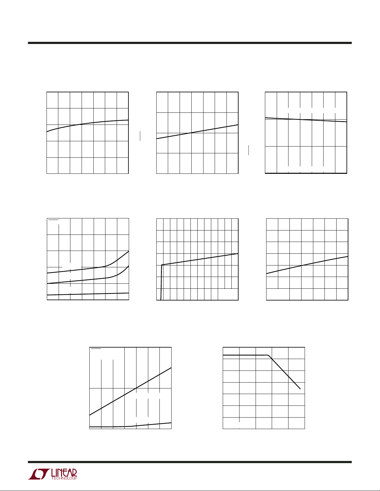
TYPICAL PERFOR A CE CHARACTERISTICS
1.28
V
vs Temperature
REF
1.60
⎯S⎯H⎯D⎯
N Threshold vs Temperature
LT3478/LT3478-1
⎯S⎯H⎯D⎯
N Pin (Hysteresis) Current vs
Temperature
15
1.26
1.24
(V)
REF
V
1.22
1.20
1.18
–50
–25 0 25
JUNCTION TEMPERATURE (°C)
Shutdown Current vs
V
IN
50 75 100 125
3478 G07
Temperature V
50
SHDN = 0V
40
30
20
CURRENT (µA)
IN
V
10
0
–50
VIN = 36V
VIN = 20V
VIN = 2.8V
–25 0 25
JUNCTION TEMPERATURE (°C)
50 75 100 125
3478 G10
1.50
1.40
SHDN (V)
1.30
1.20
–50
IN
14
12
10
8
6
CURRENT (mA)
IN
V
4
2
0
36 12
0
–25 0 25
JUNCTION TEMPERATURE (°C)
50 75 100 125
Quiescent Current vs V
18 272491521 303336
VIN (V)
3478 G08
IN
TA= 25°C
= 0V
V
C
3478 G11
JUST BEFORE PART TURNS ON
10
5
SHDN PIN CURRENT (µA)
0
–50
AFTER PART TURNS ON
–25 0 25
JUNCTION TEMPERATURE (°C)
VIN Quiescent Current vs
Temperature
14
12
10
8
6
CURRENT (mA)
IN
V
4
2
VIN = 2.8V
= 0V
V
C
0
–50
–25 0 25
JUNCTION TEMPERATURE (°C)
50 75 100 125
3478 G09
50 75 100 125
3478 G12
VS, L, SW Shutdown Currents vs
Temperature
4
SHDN = 0V
= L = SW = 36V
V
S
2
I(VS PIN) = I(L PIN)
PIN CURRENT (µA)
I(SW PIN)
0
–50
–25 0 25
JUNCTION TEMPERATURE (°C)
50 75 100 125
3478 G18
Switch Peak Current Limit
vs Duty Cycle
7
6
5
4
3
2
1
SWITCH PEAK CURRENT LIMIT (A)
TA= 25°C
0
20
0
40 60 80 100
DUTY CYCLE (%)
3478 G19
34781f
5
LT3478/LT3478-1
UW
TYPICAL PERFOR A CE CHARACTERISTICS
Switching Frequency vs R
10000
TA = 25°C
1000
SWITCHING FREQUENCY (kHz)
100
1
10 100 1000
RT (kΩ)
T
3478 G13
SS Pin Charge Current vs
Temperature
14
13
Switching Frequency vs
Temperature
1.20
RT = 31.6k
1.15
1.10
1.05
1.00
0.95
0.90
SWITCHING FREQUENCY (MHz)
0.85
0.80
–25 0 25
–50
JUNCTION TEMPERATURE (°C)
50 75 100 125
3478 G14
Pin Active and Clamp Voltages
V
C
vs Temperature
1.8
1.5
1.2
Open-Circuit Output Clamp
Voltage vs Temperature
43.0
OVPSET = 1V
42.5
42.0
41.5
41.0
CLAMP (V)
40.5
OUT
V
40.0
39.5
39.0
–25 0 25
–50
JUNCTION TEMPERATURE (°C)
VC CLAMP
50 75 100 125
3478 G15
12
11
SS PIN CURRENT (µA) (OUT OF PIN)
10
–50
–25 0 25
JUNCTION TEMPERATURE (°C)
50 75 100 125
3478 G16
(V)
C
V
0.9
0.6
0.3
0
–50
VC ACTIVE THRESHOLD
–25 0 25
JUNCTION TEMPERATURE (°C)
50 75 100 125
3478 G17
6
34781f

PI FU CTIO S
LT3478/LT3478-1
UUU
SW (Pins 1, 2): Switch Pin. Collector of the internal NPN
power switch. Both pins are fused together inside the IC.
Connect the inductor and diode here and minimize the
metal trace area connected to this pin to minimize EMI.
(Pin 3): Input Supply. Must be locally bypassed with
V
IN
a capacitor to ground.
(Pin 4): Inductor Supply. Must be locally bypassed
V
S
with a capacitor to ground. Can be shorted to V
if only
IN
one supply is available (see L (Pin 5) function).
L (Pin 5): Inductor Pin. An internal resistor between V
S
and L pins monitors inductor current to protect against
inrush current. Exceeding 6A immediately turns off the
internal NPN power switch and discharges the soft-start
pin. Input current monitoring can be disabled by connecting the inductor power supply directly to the L pin and
leaving the V
to GND on L pin; not V
(Pin 6): Output voltage of the converter. Connect a
V
OUT
pin open (requires local bypass capacitor
S
pin).
S
capacitor from this pin to ground. Internal circuitry monitors V
for protection against open LED faults.
OUT
LED (Pin 7): Connect the LED string from this pin to
ground. An internal (LT3478-1)/external (LT3478) resistor
between the V
and LED pins senses LED current for
OUT
accurate control.
OVPSET (Pin 8): Programs V
overvoltage protection
OUT
level (OVP) to protect against open LED faults. OVP =
(OVPSET • 41)V. OVPSET range is 0.3V to 1V for an OVP
range of typically 12.3V to 41V.
(Pin 9): Output of the transconductance error amplifi er
V
C
and compensation pin for the converter regulation loop.
(Pin 10): Bandgap Voltage Reference. This pin can
V
REF
supply up to 100µA. Can be used to program CTRL1,
CTRL2, OVPSET pin voltages using resistor dividers to
ground.
⎯S⎯H⎯D⎯
N (Pin 11): The ⎯S⎯H⎯D⎯N pin has an accurate 1.4V
threshold and can be used to program an undervoltage
lockout (UVLO) threshold for system input supply using a
resistor divider from supply to ground. A 10µA pin current
hysteresis allows programming of undervoltage lockout
⎯S⎯H⎯D⎯
(UVLO) hysteresis.
and removes a 10µA sink current from the pin.
reduces V
to V
IN
current < 3µA. ⎯S⎯H⎯D⎯N can be directly connected
IN
. If left open circuit the part will be turned off.
N above 1.4V turns the part on
⎯S⎯H⎯D⎯
N = 0V
CTRL1 (Pin 12): CTRL1 pin voltage is used to program
maximum LED current (CTRL2 = V
can be set by a resistor divider from V
). CTRL1 voltage
REF
or an external
REF
voltage source. Maximum LED current is given by:
(LT3478-1) Max LED Current = Min(CTRL1, 1.05) Amps
()
LT Max LED Current
3478
(,.)•
Min CTRL
105
01
R
SE
(linear for 0.1V < CTRL1< 0.95V ; CTRL2 = V
mum LED current, short CTRL1 and CTRL2 pins to V
.
NNSE
=
Amps
) For maxi-
REF
REF
.
CTRL2 (Pin 13): The CTRL2 pin is available for programming a decrease in LED current versus temperature
(setting temperature breakpoint and slope). This feature
allows the output LED(s) to be programmed for maximum
allowable current without damage at higher temperatures.
This maximizes LED usage and increases reliability. A
CTRL2 voltage with negative temperature coeffi cient is
created using an external resistor divider from V
REF
with
temperature dependant resistance. If not used, CTRL2
should be tied to V
REF
.
PWM (Pin 14): Input pin for PWM dimming control. Above
1V allows converter switching and below 1V disables
switching with V
pin level maintained. With an external
C
MOSFET placed in series with the ground side of the LED
string, a PWM signal driving the PWM pin and MOSFET
gate provides accurate dimming control. The PWM signal
can be driven from 0V to 15V. If unused, the pin should
be connected to V
(Pin 15): A resistor to ground programs switching
R
T
REF
.
frequency between 200kHz and 2.25MHz.
SS (Pin 16): Soft-Start Pin. Placing a capacitor here programs soft-start timing to limit inductor inrush current
during start-up due to the converter. When inductor current
34781f
7
LT3478/LT3478-1
UUU
PI FU CTIO S
exceeds 6A or V
exceeds OVP, an internal soft-start
OUT
latch is set, the power NPN is immediately turned off and
the SS pin is discharged. The soft-start latch is also set
and/or ⎯S⎯H⎯D⎯N do not meet their turn on thresholds.
if V
IN
The SS pin only recharges when all faults are removed
and the pin has been discharged below 0.25V.
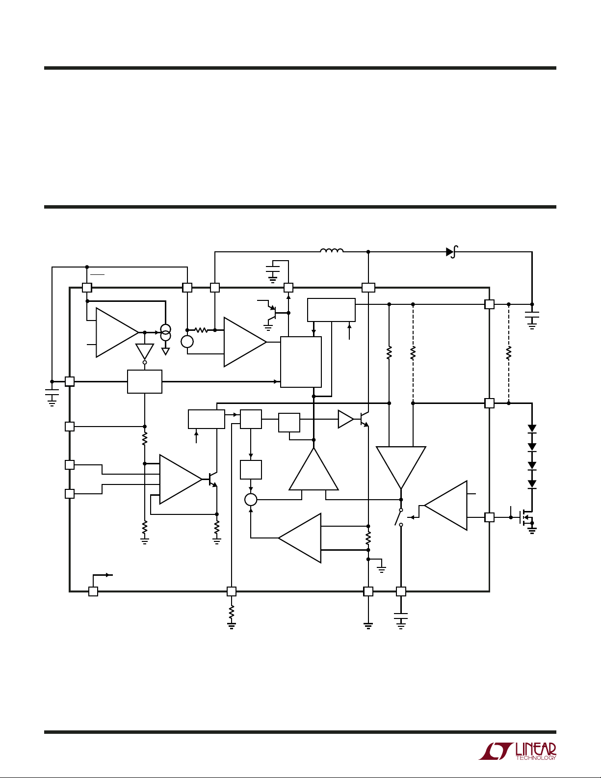
W
BLOCK DIAGRA
SHDN
11
10µA
4
–
UVLO
+
–
1.4V
+
V
IN
3
V
REF
10
REF
1.24V
V
S
5
9.5mΩ
57mV
INRUSH
CURRENT
PROTECTION
PWM
DETECT
L
V
C
–
+
OSC SQ Q1
SS
16
SOFT-START
R
Exposed Pad (Pin 17): The ground for the IC and the converter. The FE package has an Exposed Pad underneath the
IC which is the best path for heat out of the package. Pin 17
should be soldered to a continuous copper ground plane
under the device to reduce die temperature and increase
the power capability of the LT3478/LT3478-1.
SW
OVERVOLTAGE
DETECT
OVPSET
1, 2
100Ω R
SENSE
0.1Ω
(INTERNAL FOR
LT3478-1)
V
OUT
6
LED
7
R
SENSE
(EXTERNAL FOR
LT3478)
LED
CTRL1
CTRL2
–
12
13
8
OVPSET
1.05V
TO OVERVOLTAGE
DETECT CIRCUIT
PWM
+
+
+
–
1000Ω
SLOPE
COMP
Q2
Σ
+
–
+
R
–
15
R
T
EXPOSED PAD
S
17
(GND)
+
GM
–
1V
PWM
+
14
9
V
C
3478 F01
LED
LED
LED
Figure 1
34781f
8

OPERATIO
LT3478/LT3478-1
U
The LT3478/LT3478-1 are high powered LED drivers with
a 42V, 4.5A internal switch and the ability to drive LEDs
with up to 1050mA for LT3478-1 and up to 105mV/R
for LT3478.
The LT3478/LT3478-1 work similarly to a conventional
current mode boost converter but use LED current (instead
of output voltage) as feedback for the control loop. The
Block Diagram in Figure 1 shows the major functions of
the LT3478/LT3478-1.
For the part to turn on, the V
⎯S⎯H⎯D⎯
the
allows programming of an undervoltage lockout (UVLO)
threshold for the system input supply using a simple
resistor divider. A 10µA current fl ows into the
before part turn on and is removed after part turn on. This
current hysteresis allows programming of hysteresis for
the UVLO threshold. See “Shutdown Pin and Programming
Undervoltage Lockout” in the Applications Information
Section. For micropower shutdown the
reduces V
Each LED driver is a current mode step-up switching regulator. A regulation point is achieved when the
boosted output voltage V
high enough to create current in the LED(s) equal to the
programmed LED current. A sense resistor connected in
series with the LED(s) provides feedback of LED current
to the converter loop.
The basic loop uses a pulse from an internal oscillator to set
the RS fl ip-fl op and turn on the internal power NPN switch
Q1 connected between the switch pin, SW, and ground.
Current increases in the external inductor until switch
current limit is exceeded or until the oscillator reaches
its maximum duty cycle. The switch is then turned off,
causing inductor current to lift the SW pin and turn on an
external Schottky diode connected to the output. Inductor
current fl ows via the Schottky diode charging the output
capacitor. The switch is turned back on at the next reset
cycle of the internal oscillator. During normal operation
N pin must exceed 1.4V. The ⎯S⎯H⎯D⎯N pin threshold
supply current to approximately 3µA.
IN
pin must exceed 2.8V and
IN
⎯S⎯H⎯D⎯
⎯S⎯H⎯D⎯
N pin at 0V
across the output LED(s) is
OUT
SENSE
N pin
voltage controls the peak switch current limit and
the V
C
hence the inductor current available to the output LED(s).
As with all current mode converters, slope compensation
is added to the control path to ensure stability.
The CTRL1 pin is used to program maximum LED current
via Q2. The CTRL2 pin can be used to program a decrease
in LED current versus temperature for maximum reliability
and utilization of the LED(s). A CTRL2 voltage with negative
temperature coeffi cient can be created using an external
resistor divider from V
resistance. Unused CTRL2 is tied to V
For True Color PWM dimming, the LT3478/LT3478-1
provide up to a 3000:1 wide PWM dimming range by allowing the duty cycle of the PWM pin (connected to the
IC and an external N-channel MOSFET in series with the
LED(s)) to be reduced from 100% to as low as 0.033%
for a PWM frequency of 100Hz. Dimming by PWM duty
cycle, allows for constant LED color to be maintained over
the entire dimming range.
For robust operation, the LT3478/LT3478-1 monitor system
performance for any of the following faults : V
pin voltages too low and/or inductor current too high
and/or boosted output voltage too high. On detection of
any of these faults, the LT3478/LT3478-1 stop switching
immediately and a soft-start latch is set discharging the
SS pin (see Timing Diagram for SS pin in Figure 11). All
faults are detected internally and do not require external
components. When all faults no longer exist, an internal
12µA supply charges the SS pin with a timing programmed
using a single external capacitor. A gradual ramp up of SS
pin voltage limits switch current during startup.
For optimum component sizing, duty cycle range and effi ciency the LT3478/LT3478-1 allow for a separate inductor
supply V
from 200kHz up to 2.25MHz using a resistor from the R
pin to ground. The advantages of these options are covered
in the Applications Informations section.
and for switching frequency to be programmed
S
with temperature dependant
REF
.
REF
or ⎯S⎯H⎯D⎯N
IN
T
34781f
9

LT3478/LT3478-1
U
WUU
APPLICATIO S I FOR ATIO
Inductor Selection
Several inductors that work well with the LT3478/LT3478-1
are listed in Table 1. However, there are many other manufacturers and inductors that can be used. Consult each
manufacturer for more detailed information and their entire
range of parts. Ferrite cores should be used to obtain the
best effi ciency. Choose an inductor that can handle the
necessary peak current without saturating. Also ensure
that the inductor has a low DCR (copper-wire resistance)
to minimize I
22µH will suffi ce for most applications.
Inductor manufacturers specify the maximum current
rating as the current where inductance falls by a given
percentage of its nominal value. An inductor can pass a
current greater than its rated value without damaging it.
Aggressive designs where board space is precious will
exceed the maximum current rating of the inductor to save
space. Consult each manufacturer to determine how the
maximum inductor current is measured and how much
more current the inductor can reliably conduct.
2
R power losses. Values between 4.7µH and
Capacitor Selection
Low ESR (equivalent series resistance) ceramic capacitors should be used at the output to minimize the output
ripple voltage. Use only X5R or X7R dielectrics, as these
materials retain their capacitance over wider voltage and
temperature ranges than other dielectrics. A 4.7µF to
10µF output capacitor is suffi cient for most high output
current designs. Some suggested manufacturers are
listed in Table 2.
Diode Selection
Schottky diodes, with their low forward voltage drop and
fast switching speed, are ideal for LT3478/LT3478-1 applications. Table 3 lists several Schottky diodes that work
well. The diode’s average current rating must exceed the
application’s average output current. The diode’s maximum
reverse voltage must exceed the application’s output voltage. A 4.5A diode is suffi cient for most designs. For PWM
dimming applications, be aware of the reverse leakage
current of the diode. Lower leakage current will drain the
output capacitor less, allowing for higher dimming range.
The companies below offer Schottky diodes with high
voltage and current ratings.
Table 1. Suggested Inductors
MANUFACTURER PART NUMBER IDC (A) INDUCTANCE (µH) MAX DCR (mΩ)L × W × H (mm) MANUFACTURER
CDRH104R-100NC
CDRH103RNP-4R7NC-B
CDRH124R-100MC
CDRH104R-5R2NC
FDV0630-4R7M 4.2 4.7 49 7.0 × 7.7 × 3.0 Toko
UP4B-220 7.6 22 34 22 × 15 × 7.9 Cooper
Table 2. Ceramic Capacitor Manufacturers
MANUFACTURER PHONE NUMBER WEB
Taiyo Yuden (408) 573-4150 www.t-yuden.com
AVX (803) 448-9411 www.avxcorp.com
Murata (714) 852-2001 www.murata.com
Table 3. Suggested Diodes
MANUFACTURER PART NUMBER MAX CURRENT (A) MAX REVERSE VOLTAGE WEB
UPS340 3 40 Microsemi
B520C
B530C
B340A
B540C
PDS560
3.8
4
4.5
5.5
5
5
3
5
5
10
4.7
10
5.2
35
30
28
22
30
30
40
40
60
10.5 × 10.3 × 4.0
10.5 × 10.3 × 3.1
12.3 × 12.3 × 4.5
10.5 × 10.3 × 4.0
Sumida
www.sumida.com
www.toko.com
www.cooperet.com
www.microsemi.com
Diodes, Inc.
www.diodes.com
34781f
10

LT3478/LT3478-1
U
WUU
APPLICATIO S I FOR ATIO
Shutdown and Programming Undervoltage Lockout
The LT3478/LT3478-1 have an accurate 1.4V shutdown
⎯S⎯H⎯D⎯
threshold at the
conjunction with a resistor divider from the system input
supply to defi ne an accurate undervoltage lockout (UVLO)
threshold for the system (Figure 2).
hysteresis allows programming of hysteresis voltage for
this UVLO threshold. Just before part turn on, 10µA fl ows
⎯S⎯H⎯D⎯
into the
⎯S⎯H⎯D⎯
N pin. Calculation of the on/off thresholds for a system
N pin. After part turn on, 0µA fl ows from the
input supply using the LT3478/LT3478-1
be made as follows:
V
SUPPLY
V
SUPPLY
OFF = 1.4 [1 + R1/R2)]
ON = V
An open drain transistor can be added to the resistor
divider network at the
the turn off of the LT3478/LT3478-1.
N pin. This threshold can be used in
⎯S⎯H⎯D⎯
N pin current
⎯S⎯H⎯D⎯
N pin can
OFF + (10µA • R1)
SUPPLY
⎯S⎯H⎯D⎯
N pin to independently control
Programming Switching Frequency
The switching frequency is programmed using an external
resistor (R
) connected between the RT pin and ground. The
T
internal free-running oscillator is programmable between
200kHz and 2.25MHz. Table 4 shows the typical R
values
T
required for a range of switching frequencies.
Selecting the optimum switching frequency depends
on several factors. Inductor size is reduced with higher
frequency but effi ciency drops due to higher switching
losses. In addition, some applications require very high duty
cycles to drive a large number of LEDs from a low supply.
Low switching frequency allows a greater operational duty
cycle and hence a greater number of LEDs to be driven.
In each case the switching frequency can be tailored to
provide the optimum solution. When programming the
switching frequency the total power losses within the IC
should be considered. See “Thermal Calculations” in the
Applications Information section.
V
SUPPLY
R1
R2
ONOFF
Figure 2. Programming Undervoltage Lockout (UVLO)
with Hysteresis
SHDN
11
1.4V
10µA
–
+
3478 F02
With the ⎯S⎯H⎯D⎯N pin connected directly to the VIN pin, an
internal undervoltage lockout threshold exists for the V
IN
pin (2.8V max). This prevents the converter from operating in an erratic mode when supply voltage is too low.
The LT3478/LT3478-1 provide a soft-start function when
⎯S⎯H⎯D⎯
recovering from such faults as
N <1.4V and/or VIN
<2.8V. See details in the Applications Information section
“Soft-Start”.
10000
TA = 25°C
1000
SWITCHING FREQUENCY (kHz)
100
1
Figure 3. Switching Frequency vs RT Resistor Value
Table 4. Switching Frequencies vs R
SWITCHING FREQUENCY (MHz) RT (kΩ)
2.25 9.09
0.2 200
10 100 1000
RT (kΩ)
Values
T
1 31.6
3478 F03
34781f
11

LT3478/LT3478-1
U
WUU
APPLICATIO S I FOR ATIO
Programming Maximum LED current
Maximum LED current can be programmed using the CTRL1
pin with CTRL2 tied to the V
The maximum allowed LED current is defi ned as:
(LT3478-1) Max LED Current = Min(CTRL1, 1.05) Amps
()
LT Max LED Current
3478
.
(,.)•
Min CTRL
1105
01
R
S
EENSE
LED current vs CTRL1 is linear for approximately
0.1V < CTRL1 < 0.95V
For maximum possible LED current, connect CTRL1 and
CTRL2 to the V
1400
1050
pin.
REF
TA = 25°C
CTRL2 = V
REF
(FOR LT3478 SCALE
BY 0.1Ω/R
SENSE
pin (see Figures 4 and 5).
REF
=
Amps
)
maximum allowed LED current versus temperature to
warn against exceeding this current limit and damaging
the LED (Figure 6).
Luxeon V (Maximum) and LT3478-1
(Programmed) Current Derating
Curves vs Temperature
900
800
700
600
500
EXAMPLE
400
LT3478-1
300
PROGRAMMED LED
FORWARD CURRENT (mA)
f
I
CURRENT DERATING CURVE
200
100
0
0
LUXEON V EMITTER
(GREEN, CYAN, BLUE, ROYAL BLUE)
θ
25
TA AMBIENT TEMPERATURE (°C)
= 20°C/W
JA
LUXEON V EMITTER
CURRENT DERATING
CURVE
50 75 100
3478 F06
700
LED CURRENT (mA)
350
0
0
LT3478-1
0.35 0.70 1.05
CTRL1 (V)
V
REF
1.40
3478 F04
Figure 4. LED Current vs CTRL1 Voltage
LT3478/LT3478-1
10
V
REF
R2 R
R1
13
CTRL2
12
CTRL1
V
LED
3478 F05
(LT3478)
OUT
SENSE
Figure 5. Programming LED Current
Programming LED Current Derating vs Temperature
A useful feature of the LT3478/LT3478-1 is the ability
to program a derating curve for maximum LED current
versus temperature. LED data sheets provide curves of
Figure 6. LED Current Derating Curve vs Ambient Temperature
Without the ability to back off LED current as temperature
increases, many LED drivers are limited to driving the
LED(s) at only 50% or less of their maximum rated currents.
This limitation requires more LEDs to obtain the intended
brightness for the application. The LT3478/LT3478-1 allow the output LED(s) to be programmed for maximum
allowable current while still protecting the LED(s) from
excessive currents at high temperature. This is achieved
by programming a voltage at the CTRL2 pin with a negative temperature coeffi cient using a resistor divider with
temperature dependent resistance (Figures 7 and 8).
CTRL2 voltage is programmed higher than CTRL1 voltage.
This allows initial LED current to be defi ned by CTRL1.
As temperature increases, CTRL2 voltage will fall below
CTRL1 voltage causing LED currents to be controlled by
CTRL2 pin voltage. The choice of resistor ratios and use
of temperature dependent resistance in the divider for the
CTRL2 pin will defi ne the LED current curve breakpoint
and slope versus temperature (Figure 8).
A variety of resistor networks and NTC resistors with different temperature coeffi cients can be used for programming
12
34781f

LT3478/LT3478-1
U
WUU
APPLICATIO S I FOR ATIO
CTRL2 to achieve the desired CTRL2 curve vs temperature.
The current derating curve shown in Figure 6 uses the
resistor network shown in option C of Figure 7.
10
V
REF
R4
R2
R1
R
NTC
R3
R
NTC
OPTION A TO D
Figure 7. Programming LED Current Derating Curve
vs Temperature (R
1100
1000
900
800
700
600
500
400
300
200
LED CURRENT = MINIMUM
CTRL1, CTRL2 PIN VOLTAGES (mV)
OF CTRL1, CTRL2
100
R3 = OPTION C
0
0
Located on LEDs PCB)
NTC
25
TA AMBIENT TEMPERATURE (°C)
Figure 8. CTRL1, 2 Programmed Voltages vs Temperature
LT3478/LT3478-1
13
CTRL2
12
CTRL1
R
Y
R
R
X
NTC
50 75 100
CTRL1
CTRL2
R
NTC
DCBA
3478 F08
R
Y
3478 F07
R
X
to obtain a resistor’s exact values over temperature from
the manufacturer. Hand calculations of CTRL2 voltage
can then be performed at each given temperature and the
resulting CTRL2 curve plotted versus temperature. Several
iterations of resistor value calculations may be required
to achieve the desired breakpoint and slope of the LED
current derating curve.
Table 5. NTC Resistor Manufacturers/Distributors
MANUFACTURER
Murata Electronics North America www.murata.com
TDK Corporation www.tdk.com
Digi-key www.digikey.com
If calculation of CTRL2 voltage at various temperatures
gives a downward slope that is too strong, alternative
resistor networks can be chosen (B, C, D in Figure 7)
which use temperature independent resistance to reduce
the effects of the NTC resistor over temperature.
Murata Electronics provides a selection of NTC resistors
with complete data over a wide range of temperatures. In
addition, a software tool is available which allows the user
to select from different resistor networks and NTC resistor
values and then simulate the exact output voltage curve
(CTRL2 behavior) over temperature. Referred to as the
‘Murata Chip NTC Thermistor Output Voltage Simulator’,
users can log onto www.murata.com/designlib and download the software followed by instructions for creating an
output voltage V
). At any time during selection of circuit parameters
(V
REF
(CTRL2) from a specifi ed VCC supply
OUT
the user can access data on the chosen NTC resistor by
clicking on a link to the Murata catalog.
Table 5 shows a list of manufacturers/distributors of NTC
resistors. There are several other manufacturers available
and the chosen supplier should be contacted for more
detailed information. To use an NTC resistor to indicate
LED temperature it is only effective if the resistor is connected as close as possible to the LED(s). LED derating
curves shown by manufacturers are listed for ambient
temperature. The NTC resistor should be submitted to
the same ambient temperature as the LED(s). Since the
temperature dependency of an NTC resistor can be nonlinear over a wide range of temperatures it is important
The following example uses hand calculations to derive
the resistor values required for CTRL1 and CTRL2 pin
voltages to achieve a given LED current derating curve.
The resistor values obtained using the Murata simulation
tool are also provided and were used to create the derating
curve shown in Figure 6. The simulation tool illustrates
the non-linear nature of the NTC resistor temperature
coeffi cient at temperatures exceeding 50°C ambient. In
addition, the resistor divider technique using an NTC
resistor to derive CTRL2 voltage inherently has a fl attening characteristic (reduced downward slope) at higher
temperatures. To avoid LED current exceeding a maximum
34781f
13

LT3478/LT3478-1
U
WUU
APPLICATIO S I FOR ATIO
allowed level at higher temperatures, the CTRL2 voltage
curve may require a greater downward slope between
25°C and 50°C to compensate for that loss of slope at
higher temperatures.
Example: Calculate the resistor values required for generating CTRL1 and CTRL2 from V
requirements:
(a) I
(b) I
(c) I
= 700mA at 25°C
LED
derating curve breakpoint occurs at 25°C
LED
derating curve has a slope of –200mA/25°C be-
LED
tween 25°C and 50°C ambient temperature
Step1: Choose CTRL1 = 700mV for I
CTRL1 = V
R2 = R1 • [(V
For V
REF
/(1 + R2/R1)
REF
/CTRL1) – 1]
REF
= 1.24V and choosing R1 = 22.1k,
R2 = 22.1k [(1.24/0.7) – 1]
R2 = 17k (choose 16.9k)
based on the following
REF
= 700mA
LED
R
R
R
NTC
NTC
NTC
(50°C) = R
(25°C).e
NTC
(50°C) = 22k • 0.358
(50°C) = 7.9k
–1.026
CTRL2(50°C) = 1.24/(1 + 16.9/7.9) = 395mV
CTRL2 slope (25°C to 50°C) = [CTRL2(50°C)
– CTRL2(25°C)]/25°C
= (395 – 701)/25
= –306mV/25°C
I
The required I
slope = –306mA/25°C
LED
slope is –200mA/25°C. To reduce the
LED
slope of CTRL2 versus temperature it is easier to keep
the exact same NTC resistor value and B-constant (there
are limited choices) and simply adjust R4 and the type
of resistor network used for the CTRL2 pin. By changing
the resistor network to option C it is possible to place a
temperature independent resistor in series with R
reduce the effects of R
on the CTRL2 pin voltage over
NTC
NTC
to
temperature.
CTRL1 = 1.24/(1 + (16.9/22.1))
CTRL1 = 703mV (I
= 703mA)
LED
Step 2: Choose resistor network option A (Figure 7) and
CTRL2 = CTRL1 for 25°C breakpoint
start with R4 = R2 = 16.9k, R
= 22k (closest value
NTC
available)
CTRL2 = 701mV (I
= Min(CTRL1, CTRL2) • 1A =
LED
701mA)
Step 3: Calculate CTRL2 slope between 25°C and 50°C
CTRL2 (T) = 1.24/(1 + R4/R
at T = T
at T = 50°C, R
= 25°C, CTRL2 = 701mV
O
(T) = R
NTC
NTC
(T))
NTC
(TO).ex, x = B [(1/(T + 273)
– 1/298)]
(B = B-constant; linear over the 25°C to 50°C temperature
range)
For R
B-constant = 3950 and T = 50°C
NTC
x = 3950 [(1/323) – 1/298] = –1.026
Step 4: Calculate the resistor value required for R
resistor network option (c) (Figure 7) to provide an I
Y
LED
in
slope of –200mA/25°C between 25°C and 50°C ambient
temperature.
CTRL2 (25°C) = 0.7V = 1.24/(1 + (R4/(R
))
R
Y
R4 = 0.77 (R
(25°C) + RY) (a)
NTC
(25°C)+
NTC
for –200mA/25°C slope ≥ CTRL2(50°C) = 0.7 – 0.2 =
0.5
CTRL2(50°C) = 0.5V = 1.24/(1 + (R4/(R
R4 = 1.48 (R
Equating (a) = (b) and knowing R
(50°C) = 7.9k gives,
R
NTC
0.77 (22k + R
17k + 0.77 R
(50°C) + RY) (b)
NTC
(25°C) = 22k and
NTC
) = 1.48 (7.9k + RY)
Y
= 11.7 k + 1.48 R
Y
Y
NTC
+ RY))
RY = (17k – 11.7k)/(1.48 – 0.77)
R
= 7.5k
Y
14
34781f

LT3478/LT3478-1
U
WUU
APPLICATIO S I FOR ATIO
The value for R4 can now be solved using equation (a)
where,
R4 = 0.77 (R
R4 = 22.7k (choose 22.6k)
slope can now be calculated from,
I
LED
slope = [CTRL2(50°C) – CTRL2(25°C)]/25°C
I
LED
where CTRL2 (50°C) = 1.24/(1 + 22.6/(7.9 + 7.5)) =
503mV
and CTRL2 (25°C) = 1.24/(1 + 39.2/(22 + 28.7)) =
699mV
giving I
LED
= 503mV – 699mV/25°C
= –196mV/25°C => I
Using the Murata simulation tool for the resistor network
and values in the above example shows a CTRL2 voltage curve that fl attens out as temperatures approach
100°C ambient. The fi nal resistor network chosen for the
derating curve in Figure 6 used option C network with
R4 = 19.3k, R
= 3.01k. Although the CTRL2 downward slope is greater
than –200mA/25°C initially, the slope is required to avoid
exceeding maximum allowed LED currents at high ambient
temperatures (see Figure 6).
PWM Dimming
Many LED applications require an accurate control of the
brightness of the LED(s). In addition, being able to maintain a constant color over the entire dimming range can
be just as critical. For constant color LED dimming, the
LT3478/LT3478-1 provide a PWM pin and special internal
circuitry to allow up to a 3000:1 wide PWM dimming
range. With an N-channel MOSFET connected between
the LED(s) and ground and a PWM signal connected to
the gate of the MOSFET and the PWM pin (Figure 9), it
is possible to control the brightness of the LED(s) based
on PWM signal duty cycle only. This form of dimming is
superior to dimming control using an analog input voltage
(reducing CTRL1 voltage) because it allows constant color
to be maintained during dimming. The maximum current
(25°C) + RY) = 0.77 (22k + 7.5k)
NTC
slope (from 25°C to 50°C)
slope = –196mA/25°C
LED
= 22k (NCP15XW223J0SRC) and RY
NTC
for the output LED(s) is programmed for a given brightness/color and “chopped” over a PWM duty cycle range
(Figure 10) from 100% to as low as 0.033%.
D2
C
(LT3478)
R
SENSE
D1
3478 F09
OUT
3478 F10
VSLSW
V
IN
SHDN
V
REF
CTRL2
CTRL1
OVPSET
Figure 9. PWM Dimming Control Using the LT3478/LT3478-1
PWM
INDUCTOR
CURRENT
LED
CURRENT
Figure 10. PWM Dimming Waveforms Using the
LT3478/LT3478-1
LT3478/
LT3478-1
R
C
T
PWM DIMMING
CONTROL
TON
MAX I
PWM
LED
T
PWM
V
OUT
LED
PWMV
(= 1/f
)
PWM
Some general guidelines for LED Current Dimming using
the PWM pin (see Figure 10):
(1) PWM Dimming Ratio (PDR) = 1/(PWM duty cycle) =
1/(TON
PWM
• f
(2) Lower f
(use minimum f
)
PWM
allows higher PWM Dimming Ratios
PWM
= 100Hz to avoid visible fl icker and
PWM
to maximize PDR)
(3) Higher f
value improves PDR (allows lower TON
OSC
PWM
)
but will reduce effi ciency and increase internal heating. In
general, minimum operational TON
PWM
= 3 • (1/f
OSC
).
(4) Lower inductor value improves PDR
34781f
15

LT3478/LT3478-1
U
WUU
APPLICATIO S I FOR ATIO
(5) Higher output capacitor value improves PDR
(6) Choose the schottky diode (D2, Figure 9) for minimum
reverse leakage
See Typical Performance Characteristics graph “LED Current vs PWM Duty Cycle”.
Soft-Start
To limit inrush current and output voltage overshoot during startup/recovery from a fault condition, the LT3478/
LT3478-1 provide a soft-start pin SS. The SS pin is used
to program switch current ramp up timing using a capacitor to ground. The LT3478/LT3478-1 monitor system
parameters for the following faults: V
inductor current >6A and boosted output voltage >OVP.
On detection of any of these faults, the LT3478/LT3478-1
stop switching immediately and a soft-start latch is set
causing the SS pin to be discharged (see Timing Diagram
for the SS pin in Figure 11). When all faults no longer exist and the SS pin has been discharged to at least 0.25V,
the soft-start latch is reset and an internal 12µA supply
charges the SS pin. A gradual ramp up of SS pin voltage
is equivalent to a ramp up of switch current limit until SS
exceeds V
.
C
The ramp rate of the SS pin is given by:
ΔV
SW
SS
FAULTS TRIGGERING
SOFT-START LATCH
WITH SW TURNED OFF
IMMEDIATELY:
V
IN
SHDN < 1.4V OR
V
OUT
I
(INDUCTOR)
/Δt = 12µA/C
SS
< 2.8V OR
> OVP OR
> 6A
Figure 11. LT3478 Fault Detection and SS Pin Timing Diagram
SS
SOFT-START
LATCH SET:
<2.8V, ⎯S⎯H⎯D⎯N <1.4,
IN
0.65V (ACTIVE THRESHOLD)
0.25V (RESET THRESHOLD)
0.15V
SOFT-START LATCH RESET:
SS < 0.25V AND
> 2.8V AND
V
IN
SHDN > 1.4V AND
< OVP AND
V
OUT
I
(INDUCTOR)
< 6A
3478 F11
To limit inductor current overshoot to <0.5A when SS
charges past the V
level required for loop control, the CSS
C
capacitor should be chosen using the following formula:
C
SS(MIN)
Example: V
C
SS(MIN)
= 0.1µF (7.35 – 0.6(1.05 • 16/8))
= CC (7.35 – 0.6(I
= 8V, V
S
OUT
= 16V, I
• V
LED
OUT/VS
= 1.05A, CC = 0.1µF,
LED
))
= 0.612µF (choose 0.68µF).
High Inductor Current “Inrush” Protection
The LT3478/LT3478-1 provide an integrated resistor
between the V
and L pins to monitor inductor current
S
(Figure 1). During startup or “hotplugging” of the inductor supply, it is possible for inductor currents to exceed
the maximum switch current limit. When inductor current
exceeds 6A, the LT3478/LT3478-1 protect the internal
power switch by turning it off and triggering a soft-start
latch. This protection prevents the switch from repetitively
turning on during excessive inductor currents by delaying switching until the fault has been removed. To defeat
inductor current sensing the inductor supply should be
connected to the L pin and the V
pin left open. See details
S
in the Applications Information section “Soft-Start”.
LED Open Circuit Protection and Maximum PWM
Dimming Ratios
The LT3478/LT3478-1 LED drivers provide optimum protection from open LED faults by clamping the converter
output to a programmable overvoltage protection level
(OVP). In addition, the programmable OVP feature draws
zero current from the output during PWM = 0 to allow
higher PWM dimming ratios. This provides an advantage
over other LED driver applications which connect a resistor
divider directly from V
OUT
.
An open LED fault occurs when the connection to the
LED(s) becomes broken or the LED(s) fails open. For an
LED driver using a step-up switching regulator, an open
circuit LED fault can cause the converter output to exceed
the voltage capabilities of the regulator’s power switch,
causing permanent damage. When V
exceeds OVP, the
OUT
16
34781f

LT3478/LT3478-1
U
WUU
APPLICATIO S I FOR ATIO
LT3478/LT3478-1 immediately stop switching, a soft-start
latch is set and the SS pin is discharged. The SS latch can
only be reset when V
has been discharged below 0.25V (Figure 11). If the LED(s)
simply go open circuit and are reconnected, however, the
OVP used to protect the switch might be too high for the
reconnected LED(s). The LT3478/LT3478-1 therefore allow
OVP to be programmable to protect both the LED driver
switch and the LED(s). (The minimum allowable OVP for
normal operation for a given LED string depends on the
number of LEDs and their maximum forward voltage ratings.) OVP is programmed using the OVPSET pin (front
page), given by,
OVP = (OVPSET • 41)V
where the programmable range for the OVPSET pin is 0.3V
to 1V resulting in an OVP range of 12.3V to 41V.
The OVPSET pin can be programmed with a single resistor
by tapping off of the resistor divider from V
program CTRL1. If both CTRL1 and CTRL2 are connected
directly to V
(maximum LED current setting) then OVP-
REF
SET requires a simple 2 resistor divider from V
falls below OVP and the SS pin
OUT
used to
REF
REF
.
= inductor supply input
V
S
D = switch duty cycle = (V
= forward voltage drop of external Schottky diode
V
F
V
SAT
= I
L(AVE)
• R
SW
(2) Switch AC loss = P
= t
= effective switch current and switch VCE voltage
t
EFF
EFF
OUT
SW(AC)
(1/2)I
+ VF – VS)/(V
L(AVE)(VOUT
+ VF – V
OUT
+ VF)(F
overlap time during turn on and turn off = 2 • (t
)
t
VSW
t
t
f
= I
ISW
SWITCH
= SW fall/rise time = (V
VSW
= switching frequency
OSC
(3) Current sensing loss = P
P
SENSE(IL)
P
P
+ P
SENSE(IL)
SENSE(ILED)
(4) Input quiescent loss = P
rise/fall time = I
SENSE(ILED)
L(AVE)
= I
LED
2
2
• 9.5mΩ
• 0.1Ω
= I
• 2ns
L(AVE)
+ VF) • 0.7ns
OUT
=
SENSE
= VIN • IQ where
Q
OSC
ISW
SAT
)
)
+
Thermal Calculations
To maximize output power capability in an application
without exceeding the LT3478/LT3478-1 125°C maximum
operational junction temperature, it is useful to be able
to calculate power dissipation within the IC. The power
dissipation within the IC comes from four main sources:
switch DC loss, switch AC loss, Inductor and LED current sensing and input quiescent current. These formulas
assume a boost converter architecture, continuous mode
operation and no PWM dimming.
(1) Switch DC loss = P
= (RSW • I
R
I
P
= switch resistance = 0.07Ω (at TJ = 125°C)
SW
= P
L(AVE)
OUT
= V
OUT
OUT
• I
η = converter effi ciency = P
SW(DC)
/(η • VS)
LED
L(AVE)
OUT
2
/(P
• D)
OUT
+ P
LOSS
)
= (6.2mA + (100mA • D))
I
Q
Example (Using LT3478-1):
For V
V
= VS = 8V, I
IN
= 0.5V and f
F
OSC
= 700mA, V
LED
= 0.2Mhz,
= 24.5V (7 LEDs),
OUT
η = 0.89 (initial assumption)
I
= (24.5 • 0.7)/(0.89 • 8) = 2.41A
L(AVE)
D = (24.5 + 0.5 – 8)/(24.5 + 0.5 – 0.17) = 0.684
T
= 2 • ((2.41 • 2)ns + (24.5 + 0.5) • 0.7)ns = 45ns
EFF
Total Power Dissipation:
= P
P
IC
P
SW(DC)
P
SW(AC)
P
SENSE
= 8 • (6.2mA + (100mA • 0.684)) = 0.597W
P
Q
= 0.278 + 0.271 + 0.104 + 0.597 = 1.25W
P
IC
SW(DC)
+ P
SW(AC)
+ P
SENSE
+ P
Q
= 0.07 • (2.41)2 • 0.684 = 0.278W
= 45ns • 0.5 • 2.41 • 25 • 0.2MHz = 0.271W
= ((2.41)2 • 0.0095) + ((0.7)2 • 0.1) = 0.104W
34781f
17

LT3478/LT3478-1
U
WUU
APPLICATIO S I FOR ATIO
Local heating from the nearby inductor and Schottky diode
will also add to the fi nal junction temperature of the IC.
Based on empirical measurements, the effect of diode and
inductor heating on the LT3478-1 junction temperature
can be approximated as:
(LT3478-1) = 5°C/W • (P
ΔT
J
P
= (1 – D) • VF • I
DIODE
L(AVE)
1 – D = 0.316
= 0.5V
V
F
I
P
P
= 2.41
L(AVE)
= 0.316 • 0.5 • 2.41 = 0.381W
DIODE
INDUCTOR
= I
L(AVE)
2
• DCR
DCR = inductor DC resistance (assume 0.05Ω)
P
INDUCTOR
= (2.41)2 • 0.05 = 0.29W
The LT3478/LT3478-1 use a thermally enhanced FE package. With proper soldering to the Exposed Pad on the
underside of the package combined with a full copper plane
underneath the device, thermal resistance (θ
about 35°C/W. For an ambient temperature of T
the junction temperature of the LT3478-1 for the example
application described above, can be calculated as:
(LT3478-1)
T
J
= T
+ θJA(P
A
TOT
) + 5(P
DIODE
= 70 + 35(1.25) + 5(0.671)
= 70 + 44 + 4
= 118°C
In the above example, effi ciency was initially assumed to
be η = 0.89. A lower effi ciency (η) for the converter will
increase I
. η can be calculated as:
for T
J
η = P
OUT
and hence increase the calculated value
L(AVE)
/(P
OUT
+ P
LOSS
)
DIODE
+ P
+ P
INDUCTOR
INDUCTOR
JA
)
)
) will be
= 70°C,
A
If an application is built, the inductor current can be measured and a new value for junction temperature estimated.
Ideally a thermal measurement should be made to achieve
the greatest accuracy for T
.
J
Note: The junction temperature of the IC can be reduced
if a lower V
inductor supply V
from an available 3V source (instead of V
supply is available – separate from the
IN
. In the above example, driving VIN
S
= 8V) reduces
S
input quiescent losses in item(4) from 0.597W to 0.224W,
resulting in a reduction of T
from 118°C to 105°C.
J
Layout Considerations
As with all switching regulators, careful attention must be
given to PCB layout and component placement to achieve
optimal thermal,electrical and noise performance (Figure
12). The exposed pad of the LT3478/LT3478-1 (Pin 17)
is the only GND connection for the IC. The exposed pad
should be soldered to a continuous copper ground plane
underneath the device to reduce die temperature and
maximize the power capability of the IC. The ground path
for the R
resistor and VC capacitor should be taken from
T
nearby the analog ground connection to the exposed pad
(near Pin 9) separate from the power ground connection
to the exposed pad (near Pin 16). The bypass capacitor
for V
should be placed as close as possible to the VIN
IN
pin and the analog ground connection. SW pin voltage rise
and fall times are designed to be as short as possible for
maximum effi ciency. To reduce the effects of both radiated
and conducted noise, the area of the SW trace should be
kept as small as possible. Use a ground plane under the
switching regulator to minimize interplane coupling. The
schottky diode and output capacitor should be placed as
close as possible to the SW node to minimize this high
frequency switching path. To minimize LED current sensing
errors for the LT3478, the terminals of the external sense
resistor R
should be tracked to the V
SENSE
OUT
and LED
pins separate from any high current paths.
P
OUT
P
LOSS
= V
• I
OUT
= 17.15W
LED
(estimated) = PIC + P
DIODE
η = 17.15/(17.15 + 1.92) = 0.9
18
+ P
INDUCTOR
= 1.92W
34781f

LT3478/LT3478-1
U
WUU
APPLICATIO S I FOR ATIO
V
C
VS
C
VIN
SW
INDUCTOR
L
Figure 12. Recommended Layout for LT3478/LT3478-1 (Boost Confi guration)
S
V
IN
SCHOTTKY
R
SENSE
(LT3478 ONLY)
DIODE
(CONNECT MULTIPLE GROUND PLANES
THROUGH VIAS UNDERNEATH THE IC)
V
OUT
LT3478/LT3478-1
1
SW
2
SW
3
V
IN
4
V
S
5
L
6
V
OUT
EXPOSED PAD
7
LED
OVPSET
R
R
8
C
OUTPUT CAPACITOR
POWER GND
PIN 17
ANALOG GND
V
BYPASS CAP
IN
SOLDER THE EXPOSED PAD (PIN 17)
TO THE ENTIRE COPPER GROUND PLANE
UNDERNEATH THE DEVICE
SS
16
R
15
T
PWM
14
CTRL2
13
CTRL1
12
SHDN
11
V
10
REF
V
9
C
C
R
GND
F
C
C
SS
R
T
R
R
R
R
C
C
3252 F08
U
TYPICAL APPLICATIO S
V
IN
8V TO 16V
L1: CDRH104R-100NC
D1: PDS560
Q1: Si2318DS
LEDs: LUXEON III (WHITE)
3.3V
C1
4.7µF
25V
R1
45.3k
R4
54.9k
R2
130k
0V
100Hz
PWM
DIMMING RATIO = 1000:1
VINVSLSW
SHDN
V
REF
CTRL2
OVPSET
CTRL1
PWM SS V
C
1µF
LT3478-1
SS
15W, 6 LEDs at 700mA, Boost LED Driver
L1
10µH
C
f
OSC
C
0.1µF
OUT
LED
R
C
= 500kHz
R3
10k
T
D1
700mA
R
T
69.8k
C2
10µF
25V
Q1
PWM
5V/DIV
INDUCTOR
CURRENT
1A/DIV
I
LED
0.5A/DIV
LT3478-1 PWM Dimming
Waveforms
f
= 100Hz
PWM
PWM DIMMING RATIO = 1000:1
(SEE EFFICIENCY ON PAGE 1)
2µs/DIV
3478 TA02b
3478 TA02a
34781f
19

LT3478/LT3478-1
U
TYPICAL APPLICATIO S
17W, 15 LEDs at 350mA, Boost LED Driver plus LT3003
V
S
V
3.3V
C1
4.7µF
16V
IN
3.3µF
10V
100k
3.3V
0V
C3
R1
24k
R2
100Hz
PWM
DIMMING RATIO = 3000:1
VINVSLSW
SHDN
V
REF
CTRL2
CTRL1
OVPSET
PWM SS V
C
1µF
LT3478-1
SS
8V TO 14V
L1: CDRH104R-5R2
D1: PDS560
LEDs: LUXEON I (WHITE)
C
L1
5.2µH
V
C
C
0.1µF
f
OSC
C
= 1MHz
V
OUT
V
IN
OUT
LED
R
D1
V
OUT
1.05A
T
R
T
31.6k
LED1 LED2 LED3
V
MAX
V
IN
PWM
GND V
C2
3.3µF
25V
LT3003
Effi ciency vs Input V
90
VIN = 3.3V
= 350mA
I
LED
= 1MHz
f
OSC
PWM DUTY CYCLE = 100%
85
80
EFFICIENCY (%)
75
15 LEDs
(5 SERIES x 3 CHANNELS)
70
8
OT1
V
OT2
EE
C
3478 TA03a
LUXEON I (WHITE)
10 1412
VS (V)
S
3478 TA03b
V
S
12V TO 16V
V
IN
5V
L1: CDRH105R-8R2
D1: PDS560
D2: 7.5V ZENER
LEDs: LUXEON I (WHITE)
C1
4.7µF
25V
C3
3.3µF
10V
100k
3.3V
0V
R1
24k
R2
100Hz
PWM
DIMMING RATIO = 200:1
16W, 12 LEDs at 350mA, Buck-Boost Mode LED Driver plus LT3003
L1
8.2µH
VINVSLSW
SHDN
V
REF
CTRL2
CTRL1
OVPSET
PWM SS V
C
1µF
SS
LT3478-1
C
C4
1µF
V
C
C
0.1µF
f
OSC
D2
OUT
LED
C
= 500kHz
V
OUT
D1
V
OUT
1.05A
R
T
R
T
69.8k
LED1 LED2 LED3
V
MAX
V
IN
PWM
C2
10µF
50V
LT3003
GND V
OT1
V
OT2
EE
C
3478 TA04a
Effi ciency vs Input V
90
VIN = 5V
= 350mA
I
LED
85
= 500kHz
f
OSC
PWM DUTY CYCLE = 100%
80
75
70
65
EFFICIENCY (%)
60
55
50
12 14 161513
S
12 LEDs
(4 SERIES x 3 CHANNELS)
LUXEON I (WHITE)
VS (V)
3478 TA04b
34781f
20

U
TYPICAL APPLICATIO S
V
IN
3.8V TO 6.5V
NiMH 4×
L1: CDRH105R-6R8
D1: B320
Q1: Si2302ADS
Q2: Si2315BDS
LED: LUXEON III (WHITE)
3.3V
C1
10µF
10V
VINVSLSW
OFFON
R1
100k
R2
34k
0V
1kHz
SHDN
V
REF
CTRL2
CTRL1
OVPSET
PWM SS V
PWM
DIMMING RATIO = 200:1
C
1µF
LT3478-1
SS
4W, 1 LED at 1A, Buck-Boost Mode LED Driver
C
L1
6.8µH
C
C
0.1µF
f
OSC
OUT
LED
R
T
= 500kHz
D1
R
T
69.8k
C2
4.7µF
16V
1A
510Ω
510Ω
R3
10k
Q2
R4
R5
Q1
LT3478/LT3478-1
80
I
= 1A
LED
f
= 500kHz
OSC
PWM DUTY CYCLE = 100%
75
70
65
EFFICIENCY (%)
60
55
50
35764
Effi ciency vs V
VIN (V)
IN
SINGLE LED
LUXEON III (WHITE)
3478 TA06b
3478 TA06a
34781f
21

LT3478/LT3478-1
U
TYPICAL APPLICATIO S
PV
32V
TYPICAL EFFICIENCY = 90%
FOR CONDITIONS/COMPONENTS SHOWN
(PWM DUTY CYCLE = 100%, T
24W, 4 LEDs at 1.5A, Buck Mode LED Driver
IN
3.3µF
50V
C1
=25°C)
A
R
SENSE
0.068Ω
1.5A
Q2
4 LEDs
R4
365Ω
C3
10µF
25V
V
IN
3.3V
L1: CDRH105R-100
D1: PDS560
Q1: 2N7002
Q2: Si2319DS
LEDs: LXK2 (WHITE)
4.7µF
10V
C2
R1
24k
R2
100k
VINVSL OUT LED SW
SHDN
V
REF
CTRL2
CTRL1
OVPSET
C
1µF
LT3478
SS V
C
SS
C
C
0.1µF
= 500kHz
f
OSC
L1
10µH
D1
PWM
R3
10k
PWM
DIMMING RATIO = 3000:1
3.3V
R
0V
T
R
T
69.8k
3478 TA07a
R5
510Ω
Q1
100Hz
22
34781f

PACKAGE DESCRIPTIO
3.58
(.141)
U
FE Package
16-Lead Plastic TSSOP (4.4mm)
(Reference LTC DWG # 05-08-1663)
Exposed Pad Variation BC
4.90 – 5.10*
(.193 – .201)
3.58
(.141)
16 1514 13 12 11
LT3478/LT3478-1
10 9
6.60 ±0.10
4.50 ±0.10
RECOMMENDED SOLDER PAD LAYOUT
0.09 – 0.20
(.0035 – .0079)
NOTE:
1. CONTROLLING DIMENSION: MILLIMETERS
2. DIMENSIONS ARE IN
3. DRAWING NOT TO SCALE
SEE NOTE 4
0.65 BSC
4.30 – 4.50*
(.169 – .177)
0.50 – 0.75
(.020 – .030)
MILLIMETERS
(INCHES)
(.116)
0.45 ±0.05
2.94
1.05 ±0.10
1345678
2
0.25
REF
0° – 8°
0.65
(.0256)
BSC
0.195 – 0.30
(.0077 – .0118)
TYP
4. RECOMMENDED MINIMUM PCB METAL SIZE
FOR EXPOSED PAD ATTACHMENT
*DIMENSIONS DO NOT INCLUDE MOLD FLASH. MOLD FLASH
SHALL NOT EXCEED 0.150mm (.006") PER SIDE
2.94
(.116)
1.10
(.0433)
MAX
0.05 – 0.15
(.002 – .006)
FE16 (BC) TSSOP 0204
6.40
(.252)
BSC
Information furnished by Linear Technology Corporation is believed to be accurate and reliable.
However, no responsibility is assumed for its use. Linear Technology Corporation makes no representation that the interconnection of its circuits as described herein will not infringe on existing patent rights.
34781f
23

LT3478/LT3478-1
TYPICAL APPLICATIO
V
S
V
3.3V
0V
IN
4.7µF
25V
3.3µF
10V
8.25k
100Hz
C1
C3
R1
R2
10k
PWM
DIMMING RATIO = 1000:1
VINVSLSW
SHDN
V
REF
CTRL2
CTRL1
OVPSET
PWM SS V
C
SS
1µF
8V TO 16V
L1: CDRH6D28
D1: ZLLS1000
Q1: Si2318DS
LEDs: LUXEON I (WHITE)
3.3V
U
6W, 6 LEDs at 250mA, Boost LED Driver
LT3478
C
L1
10µH
C
0.1µF
f
OSC
C
OUT
LED
R
= 2MHz
R3
10k
D1
C2
3.3µF
25V
R
SENSE
0.42Ω
250mA
T
R
T
10k
Q1
Effi ciency vs Input V
100
VIN = 3.3V
= 250mA
I
LED
95
= 2MHz
f
OSC
PWM DUTY CYCLE = 100%
90
85
80
75
EFFICIENCY (%)
70
65
60
8
S
6 LEDs = LUXEON I (WHITE)
12 161410
VS (V)
3478 TA05b
3478 TA05a
RELATED PARTS
PART NUMBER DESCRIPTION COMMENTS
LT1618 Constant Current, 1.4MHz, 1.5A Boost Converter with Analog/PWM
Dimming
LT3003 Three Channel LED Ballaster with 3,000:1 True Color PWM Dimming V
LT3474 36V, 1A (I
), 2MHz,Step-Down LED Driver with 400:1 True Color
LED
PWM Dimming
LT3475 Dual 1.5A(I
), 36V, 2MHz,Step-Down LED Driver 3,000:1 True
LED
Color PWM Dimming
LT3476 Quad Output 1.5A, 2MHz High Current LED Driver with 1,000:1 True
Color PWM Dimming
LT3477 42V, 3A, 3.5MHz Boost, Buck-Boost, Buck LED Driver with Analog/
PWM Dimming
LT3479 3A, 3.5MHz Full Featured DC/DC Converter with Soft-Start and
Inrush Current Protection and Analog/PWM Dimming
LT3486 Dual 1.3A , 2MHz High Current LED Driver with 1,000:1 True Color
PWM Dimming
LTC3783 High Current LED Controller with 3,000:1 True Color PWM Dimming V
: 5V to 18V, V
V
IN
: 3V to 48V, ISD <5µA, MSOP10 Package
IN
VIN: 4V to 36V, V
VIN: 4V to 36V, V
V
: 2.8V to 16V, V
IN
Package
: 2.5V to 25V, V
V
IN
Packages
V
: 2.5V to 24V, V
IN
TSSOP16E Packages
VIN: 2.5V to 24V, V
TSSOP16E Packages
: 3V to 36V, V
IN
DFN, TSSOP16E Packages
= 36V, ISD <1µA, MS10 Package
OUT(MAX)
= 13.5V, ISD <1µA, TSSOP16E Package
OUT(MAX)
= 13.5V, ISD <1µA, TSSOP20E Package
OUT(MAX)
= 36V, ISD <10µA, 5mm × 7mm QFN
OUT(MAX)
= 40V, ISD <1µA, QFN, TSSOP20E
OUT(MAX)
= 40V, ISD <1µA, 4mm × 3mm DFN,
OUT(MAX)
= 36V, ISD <1µA, 5mm × 3mm DFN,
OUT(MAX)
= Ext FET, ISD <20µA, 5mm × 4mm
OUT(MAX)
24
Linear Technology Corporation
1630 McCarthy Blvd., Milpitas, CA 95035-7417
(408) 432-1900 ● FAX: (408) 434-0507
●
www.linear.com
34781f
LT 0107 • PRINTED IN USA
© LINEAR TECHNOLOGY CORPORATION 2007
 Loading...