

FEATURES
LT3475/LT3475-1
Dual Step-Down
1.5A LED Driver
U
DESCRIPTIO
■
True Color PWMTM Delivers Constant Color with
3000:1 Dimming Range
■
Wide Input Range: 4V to 36V Operating, 40V
Maximum
■
Accurate and Adjustable Control of LED Current
from 50mA to 1.5A
■
High Side Current Sense Allows Grounded Cathode
LED Operation
■
Open LED (LT3475) and Short Circuit Protection
■
LT3475-1 Drives LED Strings Up to 25V
■
Accurate and Adjustable 200kHz to 2MHz
Switching Frequency
■
Anti-Phase Switching Reduces Ripple
■
Uses Small Inductors and Ceramic Capacitors
■
Available in the Compact 20-Lead TSSOP Thermally
Enhanced Surface Mount Package
U
APPLICATIO S
■
Automotive and Avionic Lighting
■
Architectural Detail Lighting
■
Display Backlighting
■
Constant-Current Sources
, LT, LTC and LTM are registered trademarks of Linear Technology Corporation.
All other trademarks are the property of their respective owners. Patents Pending.
The LT®3475/LT3475-1 are dual step-down DC/DC
converters designed to operate as a constant-current
source. An internal sense resistor monitors the output
current allowing accurate current regulation ideal for
driving high current LEDs. The high side current sense allows grounded cathode LED operation. High output current
accuracy is maintained over a wide current range, from
50mA to 1.5A, allowing a wide dimming range. Unique
PWM circuitry allows a dimming range of 3000:1, avoiding the color shift normally associated with LED current
dimming.
The high switching frequency offers several advantages,
permitting the use of small inductors and ceramic capacitors. Small inductors combined with the 20 lead TSSOP
surface mount package save space and cost versus
alternative solutions. The constant switching frequency
combined with low-impedance ceramic capacitors result
in low, predictable output ripple.
With its wide input range of 4V to 36V, the LT3475/LT3475-1
regulate a broad array of power sources. A current mode
PWM architecture provides fast transient response and
cycle-by-cycle current limiting. Frequency foldback and
thermal shutdown provide additional protection.
TYPICAL APPLICATIO
Dual Step-Down 1.5A LED Driver
V
IN
2.2μF
5V TO 36V
10μH 10μH
0.1μF
1.5A LED
CURRENT
0.22μF
*DIMMING
CONTROL
4.7μF
BOOST1 BOOST2
SW1 SW2
OUT1 OUT2
LED1 LED2
PWM1 PWM2
V
C1
REF R
V
ADJ1
V
IN
LT3475
GND
SHDN
U
V
V
ADJ2
Effi ciency
95
VIN = 12V
0.22μF
DIMMING*
CONTROL
C2
T
fSW = 600kHz*SEE APPLICATIONS SECTION FOR DETAILS
24.3k
0.1μF
1.5A LED
CURRENT
2.2μF
3475 TA01
90
85
80
75
70
EFFICIENCY (%)
65
60
55
0
TWO SERIES CONNECTED
WHITE 1.5A LEDS
SINGLE WHITE 1.5A LED
0.5 1
LED CURRENT (A)
3475 TA01b
1.5
3475fb
1
LT3475/LT3475-1
WW
W
U
ABSOLUTE AXI U RATI GS
(Note 1)
VIN Pin .........................................................(-0.3V), 40V
BOOST Pin Voltage ...................................................60V
BOOST Above SW Pin ...............................................30V
OUT, LED, Pins (LT3475) ...........................................15V
OUT, LED Pins (LT3475-1) .........................................25V
PWM Pin ...................................................................15V
Pin ......................................................................6V
V
ADJ
, RT, REF Pins ..........................................................3V
V
C
SHDN Pin ...................................................................V
Maximum Junction Temperature (Note 2)............. 125°C
Operating Temperature Range (Note 3)
LT3475E/LT3475E-1 ............................. –40°C to 85°C
LT3475I/LT3475I-1 ............................. –40°C to 125°C
Storage Temperature Range ................... –65°C to 150°C
Lead Temperature Range (Soldering, 10 sec) .......300°C
IN
PIN CONFIGURATION
TOP VIEW
1
OUT1
2
LED1
3
BOOST1
4
SW1
5
V
IN
V
IN
SW2
BOOST2
LED2
OUT2
20-LEAD PLASTIC TSSOP
T
= 125°C, θJA = 30°C/W, θJC = 8°C/W
JMAX
EXPOSED PAD (PIN 21) IS GROUND AND MUST
BE ELECTRICALLY CONNECTED TO THE PCB.
6
7
8
9
10
21
FE PACKAGE
PWM1
20
V
19
ADJ1
V
18
C1
REF
17
SHDN
16
GND
15
R
14
T
V
13
C2
V
12
ADJ2
PWM2
11
ORDER INFORMATION
LEAD FREE FINISH TAPE AND REEL PART MARKING* PACKAGE DESCRIPTION TEMPERATURE RANGE
LT3475EFE#PBF LT3475EFE#TRPBF LT3475EFE 20-Lead Plastic TSSOP –40°C to 85°C
LT3475IFE#PBF LT3475IFE#TRPBF LT3475IFE 20-Lead Plastic TSSOP –40°C to 125°C
LT3475EFE-1#PBF LT3475EFE-1#TRPBF LT3475FE-1 20-Lead Plastic TSSOP –40°C to 85°C
LT3475IFE-1#PBF LT3475IFE-1#TRPBF LT3475FE-1 20-Lead Plastic TSSOP –40°C to 125°C
Consult LTC Marketing for parts specifi ed with wider operating temperature ranges. *The temperature grade is identifi ed by a label on the shipping container.
Consult LTC Marketing for information on non-standard lead based fi nish parts.
For more information on lead free part marking, go to: http://www.linear.com/leadfree/
For more information on tape and reel specifi cations, go to: http://www.linear.com/tapeandreel/
The
ELECTRICAL CHARACTERISTICS
temperature range, otherwise specifi cations are at TA = 25°C. VIN = 12V, V
PARAMETER CONDITIONS MIN TYP MAX UNITS
Minimum Input Voltage
Input Quiescent Current Not Switching 6 8 mA
Shutdown Current
SHDN = 0.3V, V
● denotes the specifi cations which apply over the full operating
BOOST
= V
OUT
BOOST
= 0V
= 16V, V
= 4V unless otherwise noted (Note 3)
OUT
●
3.7 4 V
0.01 2 μA
2
3475fb
LT3475/LT3475-1
ELECTRICAL CHARACTERISTICS
The ● denotes the specifi cations which apply over the full operating
temperature range, otherwise specifi cations are at T
= 25°C. VIN = 12V, V
A
PARAMETER CONDITIONS MIN TYP MAX UNITS
LED Pin Current V
ADJ
V
ADJ
Tied to V
Tied to V
REF
REF
• 2/3
• 7/30
LT3475E/LT3475E-1 0°C to 85°C
REF Voltage
Reference Voltage Line Regulation 4V < V
Reference Voltage Load Regulation 0 < I
Pin Bias Current (Note 4)
V
ADJ
Switching Frequency R
Maximum Duty Cycle R
Switching Phase R
Foldback Frequency R
< 40V 0.05 %/V
IN
< 500μA 0.0002 %/μA
REF
= 24.3k
T
= 24.3k
T
R
= 4.32k
T
R
= 100k
T
= 24.3k 150 180 210 Deg
T
= 24.3k, V
T
= 0V 80 kHz
OUT
SHDN Threshold (to Switch) 2.5 2.6 2.74 V
SHDN Pin Current (Note 5) V
SHDN
=
2.6V
PWM Threshold 0.3 0.8 1.2 V
Switching Threshold 0.8 V
V
C
Source Current VC = 1V 50 μA
V
C
Sink Current VC = 1V 50 μA
V
C
LED to V
LED to V
V
V
V
Transresistance 500 V/A
C
Current Gain 1 mA/μA
C
to Switch Current Gain 2.6 A/V
C
Clamp Voltage 1.8 V
C
Pin Current in PWM Mode VC = 1V, V
C
PWM
= 0.3V
OUT Pin Clamp Voltage (LT3475) 13.5 14 14.5 V
OUT Pin Current in PWM Mode V
OUT
= 4V, V
PWM
= 0.3V
Switch Current Limit (Note 6) 2.3 2.7 3.2 A
Switch V
CESAT
BOOST Pin Current I
ISW =1.5A 350 500 mV
=1.5A 25 40 mA
SW
Switch Leakage Current 0.1 10 μA
Minimum Boost Voltage Above SW 1.8 2.5 V
BOOST
= 16V, V
= 4V unless otherwise noted (Note 3)
OUT
0.97
●
0.94
0.336
0.325
●
0.31
●
1.22 1.25 1.27 V
●
●
530 600 640 kHz
●
90 95
1.00
1.03
1.04
0.350
0.364
0.375
0.385
40 400 nA
80
98
7911 μA
●
●
10 400 nA
25 50 μA
A
A
A
A
A
%
%
%
Note 1: Stresses beyond those listed under Absolute Maximum Ratings
may cause permanent damage to the device. Exposure to any Absolute
Maximum Rating condition for extended periods may affect device
reliability and lifetime.
Note 2: This IC includes overtemperature protection that is intended
to protect the device during momentary overload conditions. Junction
temperature will exceed 125°C when overtemperature protection is active.
Continuous operation above the specifi ed maximum operating junction
temperature may impair device reliability.
Note 3: The LT3475E and LT3475E-1 are guaranteed to meet performance
specifi cations from 0°C to 85°C. Specifi cations over the –40°C to 85°C
operating temperature range are assured by design, characterization and
correlation with statistical process controls. The LT3475I and LT3475I-1
are guaranteed to meet performance specifi cations over the –40°C to
125°C operating temperature range.
Note 4: Current fl ows out of pin.
Note 5: Current fl ows into pin.
Note 6: Current limit is guaranteed by design and/or correlation to static
test. Slope compensation reduces current limit at higher duty cycles.
3475fb
3
LT3475/LT3475-1
UW
TYPICAL PERFOR A CE CHARACTERISTICS
LED Current vs V
1.50
TA = 25°C
1.25
1.00
0.75
0.50
LED CURRENT (A)
0.25
0
0
0.25 0.5 0.75 1
Switch Current Limit
vs Duty Cycle
3.0
2.5
2.0
1.5
1.0
CURRENT LIMIT (A)
0.5
0
0
20 40 60 80
ADJ
V
(V)
ADJ
TYPICAL
MINIMUM
DUTY CYCLE (%)
3475 G01
TA = 25°C
3475 G04
1.25
100
LED Current vs Temperature Switch On Voltage
1.2
1.0
0.8
0.6
0.4
LED CURRENT (A)
0.2
0
–50
–25 0
V
= V
• 2/3
ADJ
REF
V
= V
ADJ
TEMPERATURE (˚C)
• 7/30
REF
50 100 125
25 75
3475 G02
600
TA = 25°C
500
400
300
200
SWITCH ON VOLTAGE (mV)
100
0
0
Switch Current Limit vs
Temperature
3.5
3.0
2.5
2.0
1.5
CURRENT LIMIT (A)
1.0
0.5
0
–50
–25 0
50 100 125
25 75
TEMPERATURE (°C)
3475 G05
Current Limit vs Output Voltage
3.0
TA = 25°C
2.5
2.0
1.5
1.0
CURRENT LIMIT (A)
0.5
0
0
0.5 1.0
SWITCH CURRENT (A)
0.5 2.5 3.0 3.52.01.0
1.5
1.5
V
(V)
OUT
2.0
3475 G03
4.0
3475 G06
Oscillator Frequency
vs Temperature
700
RT = 24.3kΩ
650
600
550
500
OSCILLATOR FREQUENCY (kHz)
450
400
–50
–25 0
TEMPERATURE (˚C)
4
50 100 125
25 75
3475 G07
Oscillator Frequency Foldback Oscillator Frequency vs R
700
TA = 25°C
= 24.3kΩ
R
T
600
500
400
300
200
OSCILLATOR FREQUENCY (kHz)
100
0
0.5 1.0 1.5 2.5
0
V
OUT
2.0
(V)
3475 G08
TA = 25°C
1000
OSCILLATOR FREQUENCY (kHz)
10
1
RT (kΩ)
T
10 100
3475 G09
3475fb
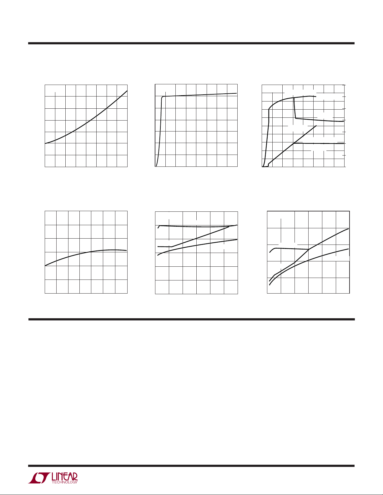
UW
TYPICAL PERFOR A CE CHARACTERISTICS
Boost Pin Current
35
TA = 25°C
30
25
20
15
10
BOOST PIN CURRENT (mA)
5
0
0.5 1.0 2.0
0
SWITCH CURRENT (A)
1.5
3475 G10
Quiescent Current
7
TA = 25°C
6
5
4
3
2
INPUT CURRENT (mA)
1
0
10 20 40
0
30
VIN (V)
3475 G11
LT3475/LT3475-1
Open-Circuit Output Voltage and
Input Current
50
TA = 25°C
45
40
35
30
25
20
15
OUTPUT VOLTAGE (V)
10
5
0
0
INPUT CURRENT
LT3475-1
10
V
LT3475-1
LT3475
OUTPUT VOLTAGE
LT3475
20
(V)
IN
14
12
INPUT CURRENT (mA)
10
8
6
4
2
0
30
40
3475 G12
Minimum Input Voltage, Single
Reference Voltage
1.28
1.27
1.26
(V)
1.25
REF
V
1.24
1.23
1.22
–50
–25 0
50 100 125
25 75
TEMPERATURE (˚C)
3475 G13
1.5A White LED
6
TA = 25°C
5
4
TO RUN
(V)
3
IN
V
2
1
0
0
0.5 1
LED CURRENT (A)
UUU
PI FU CTIO S
OUT1, OUT2 (Pins 1, 10): The OUT pin is the input to the
current sense resistor. Connect this pin to the inductor
and the output capacitor.
LED1, LED2 (Pins 2, 9): The LED pin is the output of
the current sense resistor. Connect the anode of the LED
here.
(Pins 5, 6): The VIN pins supply current to the internal
V
IN
circuitry and to the internal power switches and must be
locally bypassed.
SW1, SW2 (Pins 4, 7): The SW pin is the output of the
internal power switch. Connect this pin to the inductor,
switching diode and boost capacitor.
Minimum Input Voltage, Two Series
Connected 1.5A White LEDs
10
TA = 25°C
TO START
LED VOLTAGE
1.5
3475 G14
(V)
IN
V
9
8
7
6
5
TO RUN
0
TO START
LED VOLTAGE
0.5 1
LED CURRENT (A)
3475 G15
BOOST1, BOOST2 (Pins 3, 8): The BOOST pin is used to
provide a drive voltage, higher than the input voltage, to
the internal bipolar NPN power switch.
GND (Pins 15, Exposed Pad Pin 21): Ground. Tie the GND
pin and the exposed pad directly to the ground plane. The
exposed pad metal of the package provides both electrical
contact to ground and good thermal contact to the printed
circuit board. The exposed pad must be soldered to the
circuit board for proper operation. Use a large ground plane
and thermal vias to optimize thermal performance.
1.5
3475fb
5
LT3475/LT3475-1
UUU
PI FU CTIO S
RT (Pin 14): The RT pin is used to set the internal
oscillator frequency. Tie a 24.3k resistor from R
to GND
T
for a 600kHz switching frequency.
SHDN
(Pin 16): The
SHDN
pin is used to shut down the
switching regulator and the internal bias circuits. The
2.6V switching threshold can function as an accurate
undervoltage lockout. Pull below 0.3V to shut down the
LT3475/LT3475-1. Pull above 2.6V to enable the LT3475/
LT3475-1. Tie to V
IN
SHDN
function is unused.
if the
REF (Pin 17): The REF pin is the buffered output of the
internal reference. Either tie the REF pin to the V
ADJ
pin
for a 1.5A output current, or use a resistor divider to
generate a lower voltage at the V
pin. Leave this pin
ADJ
unconnected if unused.
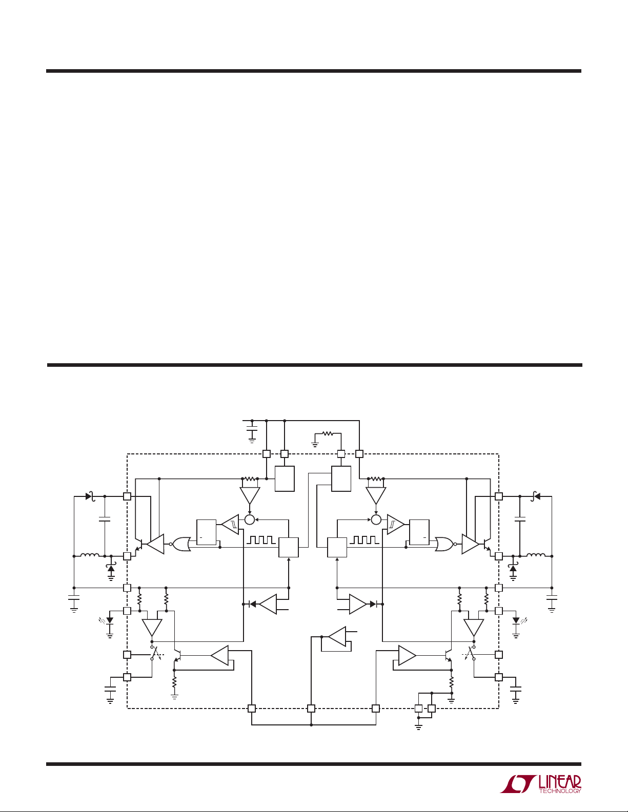
BLOCK DIAGRAM
VC1, VC2 (Pins 18, 13): The VC pin is the output of the
internal error amp. The voltage on this pin controls the
peak switch current. Use this pin to compensate the
control loop.
, V
V
ADJ1
the internal voltage-to-current amplifi er. Connect the V
(Pins 19, 12): The V
ADJ2
pin is the input to
ADJ
ADJ
pin to the REF pin for a 1.5A output current. For lower
output currents, program the V
formula: I
= 1.5A • V
LED
ADJ
/1.25V.
pin using the following
ADJ
PWM1, PWM2 (Pins 20, 11): The PWM pin controls the
connection of the V
the PWM pin is low, the V
pin to the internal circuitry. When
C
pin is disconnected from the
C
internal circuitry and draws minimal current. If the PWM
feature is unused, leave this pin unconnected.
V
IN
C
IN
V
SHDN
IN
INT REG
AND
D1 D2
BOOST1
C1 C2
Q1 Q2
SW1 SW2
L1 L2
D3 D4
C
OUT1
D
LED1
C
C1
DRIVER
OUT1
0.067Ω 100Ω 0.067Ω100Ω
LED1 LED2
gm1 gm2
PWM 1
V
C1
Q3 Q4
1.25k
C1 C2
QR
QS
∑
UVLO
SLOPE COMP SLOPE COMP
MOSC 1 MOSC 2
SLAVE
OSC
FREQUENCY
FOLDBACK
–
+
2V 2V
V
ADJ1
R
T
V
R
IN
T
MASTER
OSC
∑
SLAVE
OSC
FREQUENCY
FOLDBACK
–
+
1.25V
REF
V
ADJ2
EXPOSED
PAD
QR
QS
DRIVER
1.25k
GND
BOOST2
OUT2
PWM2
V
C2
D
LED 2
C
C
OUT2
C2
3475 BD
6
3475fb

OPERATION
LT3475/LT3475-1
The LT3475 is a dual constant frequency, current mode
regulator with internal power switches capable of generating constant 1.5A outputs. Operation can be best
understood by referring to the Block Diagram.
If the SHDN pin is tied to ground, the LT3475 is shut
down and draws minimal current from the input source
tied to V
. If the SHDN pin exceeds 1V, the internal bias
IN
circuits turn on, including the internal regulator, reference
and oscillator. The switching regulators will only begin to
operate when the SHDN pin exceeds 2.6V.
The switcher is a current mode regulator. Instead of directly
modulating the duty cycle of the power switch, the feedback
loop controls the peak current in the switch during each
cycle. Compared to voltage mode control, current mode
control improves loop dynamics and provides cycle-bycycle current limit.
A pulse from the oscillator sets the RS fl ip-fl op and turns
on the internal NPN bipolar power switch. Current in the
switch and the external inductor begins to increase. When
this current exceeds a level determined by the voltage at
VC, current comparator C1 resets the fl ip-fl op, turning
off the switch. The current in the inductor fl ows through
the external Schottky diode and begins to decrease. The
cycle begins again at the next pulse from the oscillator.
In this way, the voltage on the VC pin controls the current
through the inductor to the output. The internal error
amplifi er regulates the output current by continually
adjusting the VC pin voltage. The threshold for switching
on the VC pin is 0.8V, and an active clamp of 1.8V limits
the output current.
The voltage on the V
pin sets the current through the
ADJ
LED pin. The NPN, Q3, pulls a current proportional to the
voltage on the V
pin through the 100Ω resistor. The gm
ADJ
amplifi er servos the VC pin to set the current through the
0.067Ω resistor and the LED pin. When the voltage drop
across the 0.067Ω resistor is equal to the voltage drop
across the 100Ω resistor, the servo loop is balanced.
Tying the REF pin to the V
pin sets the LED pin current
ADJ
to 1.5A. Tying a resistor divider to the REF pin allows the
programming of LED pin currents of less than 1.5A. LED
pin current can also be programmed by tying the V
ADJ
pin
directly to a voltage source.
An LED can be dimmed with pulse width modulation
using the PWM pin and an external NFET. If the PWM
pin is unconnected or is pulled high, the part operates
nominally. If the PWM pin is pulled low, the V
pin is dis-
C
connected from the internal circuitry and draws minimal
current from the compensation capacitor. Circuitry drawing current from the OUT pin is also disabled. This way,
pin and the output capacitor store the state of
the V
C
the LED pin current until the PWM is pulled high again.
This leads to a highly linear relationship between pulse
width and output light, allowing for a large and accurate
dimming range.
pin allows programming of the switching frequency.
The R
T
For applications requiring the smallest external components
possible, a fast switching frequency can be used. If low
dropout or very high input voltages are required, a slower
switching frequency can be programmed.
During startup V
will be at a low voltage. The NPN,
OUT
Q3, can only operate correctly with suffi cient voltage
of ≈1.7V at V
the V
pin high until V
C
, A comparator senses V
OUT
rises above 2V, and Q3 is op-
OUT
and forces
OUT
erating correctly.
The switching regulator performs frequency foldback
during overload conditions. An amplifi er senses when
V
is less than 2V and begins decreasing the oscillator
OUT
frequency down from full frequency to 15% of the nominal
frequency when V
= 0V. The OUT pin is less than 2V
OUT
during startup, short circuit, and overload conditions.
Frequency foldback helps limit switch current under these
conditions.
The switch driver operates either from V
or from the
IN
BOOST pin. An external capacitor and Schottky diode
are used to generate a voltage at the BOOST pin that
is higher than the input supply. This allows the driver
to saturate the internal bipolar NPN power switch for
effi cient operation.
3475fb
7

LT3475/LT3475-1
APPLICATIONS INFORMATION
Open Circuit Protection
The LT3475 has internal open-circuit protection. If the LED
is absent or is open circuit, the LT3475 clamps the voltage
on the LED pin at 14V. The switching regulator then operates at a very low frequency to limit the input current. The
LT3475-1 has no internal open circuit protection. With the
LT3475-1, be careful not to violate the ABSMAX voltage of
th BOOST pin; if V
> 25V, external open circuit protection
IN
circuitry (as shown in Figure 1) may be necessary.The
output voltage during an open LED condition is shown in
the Typical Performance Characteristics section.
Undervoltage Lockout
Undervoltage lockout (UVLO) is typically used in situations
where the input supply is current limited, or has high source
resistance. A switching regulator draws constant power
from the source, so the source current increases as the
source voltage drops. This looks like a negative resistance
load to the source and can cause the source to current limit
or latch low under low source voltage conditions. UVLO
prevents the regulator from operating at source voltages
where these problems might occur.
An internal comparator will force the part into shutdown when V
falls below 3.7V. If an adjustable UVLO
IN
threshold is required, the SHDN pin can be used. The
threshold voltage of the SHDN pin comparator is 2.6V. An
internal resistor pulls 9μA to ground from the SHDN pin
at the UVLO threshold.
Choose resistors according to the following formula:
TH
2.6V
–2.6V
R1
–9μA
R2 =
V
VTH = UVLO Threshold
Example: Switching should not start until the input is
above 8V.
= 8V
V
TH
R1=100k
R2 =
2.6V
8V – 2.6V
= 57.6k
–9μA
100k
OUT
10k
GND
3475 F01
V
C
LT3475
V
C
3475 F02
22V
100k
Figure 1. External Overvoltage Protection
Circuitry for the LT3475-1
V
IN
C1
V
IN
R1
SHDN
R2
Figure 2. Undervoltage Lockout
2.6V
9μA
Keep the connections from the resistors to the SHDN pin
short and make sure the coupling to the SW and BOOST
pins is minimized. If high resistance values are used, the
SHDN pin should be bypassed with a 1nF capacitor to
prevent coupling problems from switching nodes.
Setting the Switching Frequency
The LT3475 uses a constant frequency architecture that
can be programmed over a 200kHz to 2MHz range with a
single external timing resistor from the R
A graph for selecting the value of R
T
pin to ground.
T
for a given operating
frequency is shown in the Typical Applications section.
Table 1. Switching Frequencies
SWITCHING FREQUENCY (MHz) RT (kΩ)
2 4.32
1.5 6.81
1.2 9.09
1 11.8
0.8 16.9
0.6 24.3
0.4 40.2
0.3 57.6
0.2 100
3475fb
8

APPLICATIONS INFORMATION
LT3475/LT3475-1
Table 1 shows suggested RT selections for a variety of
switching frequencies.
Operating Frequency Selection
The choice of operating frequency is determined by
several factors. There is a tradeoff between effi ciency and
component size. A higher switching frequency allows the
use of smaller inductors at the cost of increased switching
losses and decreased effi ciency.
Another consideration is the maximum duty cycle. In certain
applications, the converter needs to operate at a high duty
cycle in order to work at the lowest input voltage possible.
The LT3475 has a fi xed oscillator off time and a variable
on time. As a result, the maximum duty cycle increases
as the switching frequency is decreased.
Input Voltage Range
The minimum operating voltage is determined either by the
LT3475’s undervoltage lockout of 4V, or by its maximum
duty cycle. The duty cycle is the fraction of time that the
internal switch is on and is determined by the input and
output voltages:
V
OUT
+ V
F
F
DC =
VIN–VSW+ V
()
()
where VF is the forward voltage drop of the catch diode
(~0.4V) and V
is the voltage drop of the internal switch
SW
(~0.4V at maximum load). This leads to a minimum input
voltage of:
+ V
V
IN MIN
()
V
OUT
=
DC
MAX
F
–VF+ V
SW
The maximum operating voltage is determined by the
absolute maximum ratings of the V
and BOOST pins,
IN
and by the minimum duty cycle.
+ V
MIN
V
=
= t
OUT
DC
ON(MIN)
MIN
F
–VF+ V
• f
SW
is equal to 140ns and f is the switching
V
IN MAX
()
with DC
where t
ON(MIN)
frequency.
Example: f = 750kHz, V
DC
V
= 140ns • 750kHz = 0.105
MIN
3.4V + 0.4V
IN MAX
=
()
0.105
= 3.4V
OUT
– 0.4V + 0.4V = 36V
The minimum duty cycle depends on the switching frequency. Running at a lower switching frequency might
allow a higher maximum operating voltage. Note that
this is a restriction on the operating input voltage; the
circuit will tolerate transient inputs up to the Absolute
Maximum Ratings of the V
voltage should be limited to the V
and BOOST pins. The input
IN
operating range (36V)
IN
during overload conditions (short circuit or start up).
Minimum On Time
The LT3475 will regulate the output current at input voltages greater than V
IN(MAX)
. For example, an application
with an output voltage of 3V and switching frequency of
1.2MHz has a V
IN(MAX)
of 20V, as shown in Figure 3. Figure
4 shows operation at 35V. Output ripple and peak inductor
with DC
where t
= 1–t
MAX
0FF(MIN)
OFF(MIN)
is equal to 167ns and f is the switching
frequency.
Example: f = 600kHz, V
DC
V
= 1− 167ns • 600kHz = 0.90
MAX
4V + 0.4V
IN MIN
=
()
0.9
• f
= 4V
OUT
– 0.4V + 0.4V = 4.9V
V
OUT
500mV/DIV
(AC COUPLED)
1A/DIV
V
20V/DIV
I
L
SW
Figure 3. Operation at V
V
= 3V and fSW = 1.2MHHz
OUT
IN(MAX)
3475 F03
= 20V.
3475fb
9

LT3475/LT3475-1
APPLICATIONS INFORMATION
current have signifi cantly increased. Exceeding V
IN(MAX)
is safe if the external components have adequate ratings
to handle the peak conditions and if the peak inductor
current does not exceed 3.2A. A saturating inductor may
further reduce performance.
V
OUT
500mV/DIV
(AC COUPLED)
I
L
1A/DIV
V
SW
20V/DIV
3475 F04
Figure 4. Operation above V
Ripple and Peak Inductor Current Increases
IN(MAX)
. Output
Inductor Selection and Maximum Output Current
A good fi rst choice for the inductor value is:
L = (V
OUT
+ VF)•
1.2MHz
f
where VF is the voltage drop of the catch diode (~0.4V),
f is the switching frequency and L is in μH. With this value
the maximum load current will be above 1.6A at all duty
cycles. The inductor’s RMS current rating must be greater
than the maximum load current and its saturation current
should be at least 30% higher. For highest effi ciency,
the series resistance (DCR) should be less than 0.15Ω.
Table 2 lists several vendors and types that are suitable.
For robust operation at full load and high input voltages
> 30V), use an inductor with a saturation current
(V
IN
higher than 3.2A.
Table 2. Inductors
PART NUMBER
Sumida
CR43-3R3 3.3 1.44 0.086 3.5
CR43-4R7 4.7 1.15 0.109 3.5
CDRH4D16-3R3 3.3 1.10 0.063 1.8
CDRH4D28-3R3 3.3 1.57 0.049 3.0
CDRH4D28-4R7 4.7 1.32 0.072 3.0
CDRH6D26-5R0 5.0 2.20 0.032 2.8
CDRH6D26-5R6 5.6 2.0 0.036 2.8
CDRH5D28-100 10 1.30 0.048 3.0
CDRH5D28-150 15 1.10 0.076 3.0
CDRH73-100 10 1.68 0.072 3.4
CDRH73-150 15 1.33 0.130 3.4
CDRH104R-150 15 3.1 0.050 4.0
Coilcraft
DO1606T-332 3.3 1.30 0.100 2.0
DO1606T-472 4.7 1.10 0.120 2.0
DO1608C-332 3.3 2.00 0.080 2.9
DO1608C-472 4.7 1.50 0.090 2.9
MOS6020-332 3.3 1.80 0.046 2.0
MOS6020-472 10 1.50 0.050 2.0
DO3316P-103 10 3.9 0.038 5.2
DO3316P-153 15 3.1 0.046 5.2
VALUE
(μH)
I
RMS
(A)
DCR
()
HEIGHT
(mm)
The optimum inductor for a given application may differ
from the one indicated by this simple design guide. A larger
value inductor provides a higher maximum load current, and
reduces the output voltage ripple. If your load is lower than
the maximum load current, then you can relax the value of the
inductor and operate with higher ripple current. This allows
you to use a physically smaller inductor, or one with a lower
DCR resulting in higher effi ciency. In addition, low inductance
may result in discontinuous mode operation, which further
reduces maximum load current. For details of maximum
output current and discontinuous mode operation, see Linear
Technology’s Application Note 44. Finally, for duty cycles
greater than 50% (V
OUT/VIN
> 0.5), a minimum inductance
is required to avoid sub-harmonic oscillations:
10
L
= (V
MIN
OUT
+ VF)•
800kHz
f
3475fb

APPLICATIONS INFORMATION
LT3475/LT3475-1
The current in the inductor is a triangle wave with an average
value equal to the load current. The peak switch current
is equal to the output current plus half the peak-to-peak
inductor ripple current. The LT3475 limits its switch current in order to protect itself and the system from overload
faults. Therefore, the maximum output current that the
LT3475 will deliver depends on the switch current limit,
the inductor value, and the input and output voltages.
When the switch is off, the potential across the inductor
is the output voltage plus the catch diode drop. This gives
the peak-to-peak ripple current in the inductor
ΔIL=
1–DC
()
V
OUT
+ V
F
()
L•f
()
where f is the switching frequency of the LT3475 and L
is the value of the inductor. The peak inductor and switch
current is
ΔI
L
+
2
I
SW PK
= I
()
LPK
= I
()
OUT
To maintain output regulation, this peak current must be
less than the LT3475’s switch current limit I
LIM
. I
LIM
is at
least 2.3A at low duty cycles and decreases linearly to 1.8A
at DC = 0.9. The maximum output current is a function of
the chosen inductor value:
Input Capacitor Selection
Bypass the input of the LT3475 circuit with a 4.7μF or
higher ceramic capacitor of X7R or X5R type. A lower
value or a less expensive Y5V type will work if there is
additional bypassing provided by bulk electrolytic capacitors or if the input source impedance is low. The following
paragraphs describe the input capacitor considerations in
more detail.
Step-down regulators draw current from the input supply
in pulses with very fast rise and fall times. The input capacitor is required to reduce the resulting voltage ripple at
the LT3475 input and to force this switching current into a
tight local loop, minimizing EMI. The input capacitor must
have low impedance at the switching frequency to do this
effectively, and it must have an adequate ripple current rating. With two switchers operating at the same frequency
but with different phases and duty cycles, calculating the
input capacitor RMS current is not simple. However, a
conservative value is the RMS input current for the channel
• I
that is delivering most power (V
OUT
OUT
):
C
INRMS
= I
OUT
V
OUT(VIN–VOUT
•
V
IN
)
I
OUT
<
2
I
OUT MAX
= 2.3A• 1–0.25•DC
= I
()
LIM
ΔI
L
–
2
ΔI
L
()
–
2
Choosing an inductor value so that the ripple current is
small will allow a maximum output current near the switch
current limit.
One approach to choosing the inductor is to start with the
simple rule given above, look at the available inductors,
and choose one to meet cost or space goals. Then use
these equations to check that the LT3475 will be able to
deliver the required output current. Note again that these
equations assume that the inductor current is continuous. Discontinuous operation occurs when I
than ΔI
L
/2.
OUT
is less
and is largest when VIN = 2V
(50% duty cycle). As the
OUT
second, lower power channel draws input current, the
input capacitor’s RMS current actually decreases as the
out-of-phase current cancels the current drawn by the
higher power channel. Considering that the maximum
load current from a single channel is ~1.5A, RMS ripple
current will always be less than 0.75A.
The high frequency of the LT3475 reduces the energy
storage requirements of the input capacitor, so that the
capacitance required is less than 10μF. The combination
of small size and low impedance (low equivalent series
resistance or ESR) of ceramic capacitors makes them the
preferred choice. The low ESR results in very low voltage
ripple. Ceramic capacitors can handle larger magnitudes
of ripple current than other capacitor types of the same
value. Use X5R and X7R types.
3475fb
11

LT3475/LT3475-1
APPLICATIONS INFORMATION
An alternative to a high value ceramic capacitor is a
lower value ceramic along with a larger electrolytic
capacitor. The electrolytic capacitor likely needs to be greater
than 10μF in order to meet the ESR and ripple current
requirements. The input capacitor is likely to see high
surge currents when the input source is applied. Tantalum capacitors can fail due to an over-surge of current.
Only use tantalum capacitors with the appropriate surge
current rating. The manufacturer may also recommend
operation below the rated voltage of the capacitor.
A fi nal caution is in order regarding the use of ceramic
capacitors at the input. A ceramic input capacitor can
combine with stray inductance to form a resonant tank
circuit. If power is applied quickly (for example by plugging the circuit into a live power source) this tank can ring,
doubling the input voltage and damaging the LT3475. The
solution is to either clamp the input voltage or dampen the
tank circuit by adding a lossy capacitor in parallel with the
ceramic capacitor. For details, see Application Note 88.
Output Capacitor Selection
RMS current rating of the output capacitor is usually not
of concern. It can be estimated with the formula:
I
C(RM S)
= ΔIL/12
The low ESR and small size of ceramic capacitors make
them the preferred type for LT3475 applications. Not all
ceramic capacitors are the same, however. Many of the
higher value capacitors use poor dielectrics with high
temperature and voltage coeffi cients. In particular Y5V
and Z5U types lose a large fraction of their capacitance
with applied voltage and at temperature extremes.
Because loop stability and transient response depend on
the value of C
, this loss may be unacceptable. Use X7R
OUT
and X5R types. Table 3 lists several capacitor vendors.
Table 3. Low ESR Surface Mount Capacitors.
VENDOR TYPE SERIES
Taiyo-Yuden Ceramic X5R, X7R
AVX Ceramic X5R, X7R
TDK Ceramic X5R, X7R
For most LEDs, a 2.2μF, 6.3V ceramic capacitor (X5R or
X7R) at the output results in very low output voltage ripple
and good transient response. Other types and values will
also work. The following discusses tradeoffs in output
ripple and transient performance.
The output capacitor fi lters the inductor current to
generate an output with low voltage ripple. It also stores
energy in order to satisfy transient loads and stabilizes the
LT3475’s control loop. Because the LT3475 operates at a
high frequency, minimal output capacitance is necessary.
In addition, the control loop operates well with or without
the presence of output capacitor series resistance (ESR).
Ceramic capacitors, which achieve very low output ripple
and small circuit size, are therefore an option.
You can estimate output ripple with the following
equation:
V
RIPPLE
where ΔI
= ΔIL / (8 • f • C
is the peak-to-peak ripple current in the
L
) for ceramic capacitors
OUT
inductor. The RMS content of this ripple is very low so the
Diode Selection
The catch diode (D3 from the Block Diagram) conducts
current only during switch off time. Average forward current in normal operation can be calculated from:
I
D(AVG)
= I
OUT
(VIN – V
OUT
)/V
IN
The only reason to consider a diode with a larger current
rating than necessary for nominal operation is for the
worst-case condition of shorted output. The diode current will then increase to one half the typical peak switch
current limit.
Peak reverse voltage is equal to the regulator input
voltage. Use a diode with a reverse voltage rating greater
than the input voltage. Table 4 lists several Schottky
diodes and their manufacturers.
Diode reverse leakage can discharge the output capacitor
during LED off times while PWM dimming. If operating at
high ambient temperatures, use a low leakage Schottky
for the widest PWM dimming range.
12
3475fb

APPLICATIONS INFORMATION
LT3475/LT3475-1
Table 4. Schottky Diodes
V
V
R
(V)
(A)
I
AVE
(A)
at 1A
F
(mV)
V
at 2A
F
(mV)
On Semiconductor
MBR0540 40 0.5 620
MBRM120E 20 1 530
MBRM140 40 1 550
Diodes Inc
B120 20 1 500
B130 30 1 500
B140HB 40 1 530
DFLS140 40 1.1 510
B240 40 2 500
International Rectifi er
10BQ030 30 1 420
BOOST Pin Considerations
The capacitor and diode tied to the BOOST pin generate a voltage that is higher than the input voltage. In
most cases, a 0.22μF capacitor and fast switching diode
(such as the CMDSH-3 or MMSD914LT1) will work well.
Figure 5 shows three ways to arrange the boost circuit.
The BOOST pin must be more than 2.5V above the SW
pin for full effi ciency. For outputs of 3.3V and higher, the
standard circuit (Figure 5a) is best. For outputs between
2.8V and 3.3V, use a small Schottky diode (such as the
BAT-54). For lower output voltages, the boost diode can be
tied to the input (Figure 5b). The circuit in Figure 5a is more
effi cient because the BOOST pin current comes from a
lower voltage source. The anode of the boost diode can
be tied to another source that is at least 3V. For example, if
you are generating a 3.3V output, and the 3.3V output is on
whenever the LED is on, the BOOST pin can be
connected to the 3.3V output. For LT3475-1 applications
with higher output voltages, an additional Zener diode
may be necessary (Figure 5d) to maintain pin voltage
below the absolute maximum. In any case, be sure that
the maximum voltage at the BOOST pin is both less than
60V and the voltage difference between the BOOST and
SW pins is less than 30V.
The minimum operating voltage of an LT3475 application
is limited by the undervoltage lockout (~3.7V) and by the
maximum duty cycle. The boost circuit also limits the
minimum input voltage for proper start up. If the input
voltage ramps slowly, or the LT3475 turns on when the
output is already in regulation, the boost capacitor may
not be fully charged. Because the boost capacitor charges
V
BOOST
MAX V
V
BOOST
MAX V
D2
BOOST
LT3475
V
IN
– VSW≅ V
BOOST
BOOST
LT3475
V
IN
– VSW – V
BOOST
GND
IN
≅ 2V
IN
GND
Z
≅ VIN + V
(5d)
SW
SW
OUT
(5b)
– V
C3
V
OUT
D2
C3
V
OUT
3475 F05
Z
D2
BOOST
BOOST
LT3475
V
IN
– VSW≅ V
BOOST
GND
OUT
≅ VIN + V
SW
OUT
V
IN
V
MAX V
C3
V
OUT
V
IN
(5a)
V
> 3V
IN2
V
IN
D2
BOOST
LT3475
V
IN
GND
V
– VSW≅ V
BOOST
MAX V
BOOST
MINIMUM VALUE FOR V
≅ V
IN2
+ V
IN2
SW
C3
V
OUT
3475 F05
IN
=
3V
IN2
V
IN
(5c)
Figure 5. Generating the Boost Voltage
3475fb
13

LT3475/LT3475-1
APPLICATIONS INFORMATION
with the energy stored in the inductor, the circuit will rely
on some minimum load current to get the boost circuit
running properly. This minimum load will depend on input
and output voltages, and on the arrangement of the boost
circuit. The minimum load current generally goes to zero
once the circuit has started. The typical performance characteristics section shows a plot of minimum load to start
and to run as a function of input voltage. Even without an
output load current, in many cases the discharged output
capacitor will present a load to the switcher that will allow
it to start. The plots show the worst case, where V
IN
is
ramping very slowly.
Programming LED Current
The LED current can be set by adjusting the voltage on the
pin. For a 1.5A LED current, either tie V
V
ADJ
to REF or
ADJ
to a 1.25V source. For lower output currents, program the
using the following formula: I
V
ADJ
= 1.5A • V
LED
ADJ
/1.25V.
Voltages less than 1.25V can be generated with a voltage
divider from the REF pin, as shown in Figure 6. In order
to have accurate LED current, precision resistors are
preferred (1% or better is recommended). Note that the
pin sources a small amount of bias current, so use
V
ADJ
the following formula to choose resistors:
the voltage on the V
pin by tying a low on resistance
ADJ
FET to the resistor divider string. This allows the selection of two different LED currents. For reliable operation program an LED current of no less than 50mA.
The maximum current dimming ratio (I
calculated from the maximum LED current (I
minimum LED current (I
I
MAX/IMIN
= I
RATIO
) as follows:
MIN
RATIO
MAX
) can be
) and the
Another dimming control circuit (Figure 8) uses the PWM
pin and an external NFET tied to the cathode of the LED.
An external PWM signal is applied to the PWM pin and the
gate of the NFET (For PWM dimming ratios of 20 to 1 or
less, the NFET can be omitted). The average LED current is
proportional to the duty cycle of the PWM signal. When the
PWM signal goes low, the NFET turns off, turning off the
LED and leaving the output capacitor charged. The PWM
pin is pulled low as well, which disconnects the V
pin,
C
storing the voltage in the capacitor tied there. Use the C-RC
string shown in Figure 8 and Figure 9 tied to the V
pin for
C
proper operation during startup. When the PWM pin goes
high again, the LED current returns rapidly to its previous
on state since the compensation and output capacitors are
at the correct voltage. This fast settling time allows the
R2 =
1.25V – V
To minimize the error from variations in V
R1
V
ADJ
ADJ
+ 50nA
pin current,
ADJ
use resistors with a parallel resistance of less than 4k. Use
resistor strings with a high enough series resistance so as not
to exceed the 500μA current compliance of the REF pin.
Dimming Control
There are several different types of dimming control
circuits. One dimming control circuit (Figure 7) changes
REF
R1
R2
Figure 6. Setting V
LT3475
V
ADJ
GND
3475 F06
with a Resistor Divider
ADJ
REF
R1
R2
DIM
Figure 7. Dimming with a MOSFET and Resistor Divider
PWM
100Hz TO
10kHz
Figure 8. Dimming Using PWM Signal
PWM
LED
V
ADJ
LT3475
GND
LT3475
GND
V
C
3475 F08
3475 F07
3.3nF
10k
0.1μF
3475fb
14

F
APPLICATIONS INFORMATION
LT3475/LT3475-1
LT3475 to maintain diode current regulation with PWM
pulse widths as short as 7.5 switching cycles (12.5μs for
= 600kHz). Maximum PWM period is determined by
f
SW
the system and is unlikely to be longer than 12ms. Using
PWM periods shorter than 100μs is not recommended.
The maximum PWM dimming ratio (PWM
calculated from the maximum PWM period (t
minimum PWM pulse width (t
t
MAX/tMIN
Total dimming ratio (DIM
= PWM
RATIO
RATIO
) as follows:
MIN
) is the product of the PWM
RATIO
) can be
) and
MAX
dimming ratio and the current dimming ratio.
Example:
I
t
I
PWM
DIM
= 1A, I
MAX
= 3.3μs (fSW = 1.4MHz)
MIN
= 1A/0.1A =10:1
RATIO
RATIO
RATIO
MIN
= 0.1A, t
MAX
= 9.9ms
= 9.9ms/3.3μs = 3000:1
= 10 • 3000 = 30000:1
To achieve the maximum PWM dimming ratio, use the
circuit shown in Figure 9. This allows PWM pulse widths
as short as 4.5 switching cycles (7.5μs for f
= 600kHz).
SW
Note that if you use the circuit in Figure 9, the rising edge
of the two PWM signals must align within 100ns.
220pF
R
T
1M
PWM1
Figure 9. Extending the PWM Dimming Range
R
T
LT3475
GND
V
3475 F09
C
3.3nF
10k
0.1μ
Layout Hints
As with all switching regulators, careful attention must
be paid to the PCB layout and component placement. To
maximize effi ciency, switch rise and fall times are made
as short as possible. To prevent electromagnetic interference (EMI) problems, proper layout of the high frequency
switching path is essential. The voltage signal of the SW
and BOOST pins have sharp rise and fall edges. Minimize
the area of all traces connected to the BOOST and SW
pins and always use a ground plane under the switching
regulator to minimize interplane coupling. In addition, the
ground connection for frequency setting resistor R
capacitors at V
, VC2 pins (refer to the Block Diagram)
C1
and
T
should be tied directly to the GND pin and not shared
with the power ground path, ensuring a clean, noise-free
connection.
PWM2SHDNPWM1
201918171615141312
123456789
V
IN
VIA TO LOCAL GND PLANE
Figure 10. Recommended Component Placement
11
10
3475 F10
3475fb
15

LT3475/LT3475-1
TYPICAL APPLICATIONS
V
5V TO 36V
D3
L2
μH
10
C5
2.2μF
6.3V
LED 1 LED 2
0.1
C1 TO C5: X5R OR X7R
D1, D2: DFLS140
D3, D4: MBR0540
LED CURRENT = 1A
Dual Step-Down 1A LED Driver
IN
C1
μF
4.7
50V
C4
0.22μF
6.3V
D1
C6
μF
R2
1k
R3
2k
V
IN
BOOST1 BOOST2
SW1
OUT1 OUT2
LED1 LED2
V
C1
REF R
V
ADJ1
LT3475
GND
SHDN
V
SW2
V
ADJ2
C2
T
C3
0.22
μF
6.3V
0.1μF
R1
24.3k
fSW = 600kHz
D4
L1
10μH
D2
C2
μF
2.2
6.3V
C7
3475 TA02
CURRENT
Dual Step-Down 1.5A LED Driver with 1200 : 1 True Color PWM Dimming
V
IN
6V TO 36V
D3
L2
10
C4
μF
2.2
6.3V
LED 11.5A LED
R3
10k
M1 M2
D1, D2: B260
D3, D4: MBR0540
C1 TO C5: X5R OR X7R
M1, M2: Si2302ADS
M3: 2n7002L
C8
0.1
μF
PWM1 PWM2
C1
μF
4.7
50V
C2
0.22μF
C6
3.3nF
6.3V
D1
μH
V
IN
BOOST1 BOOST2
LT3475
SW1
OUT1 OUT2
LED1 LED2
PWM1 PWM2
V
C1
REF
V
ADJ1
GND
C8
220p
M3
SHDN
1M
R2
V
SW2
V
ADJ2
D4
C3
0.22
μF
6.3V
D2
C2
R
T
10μH
C7
3.3nF
R1
24.3k
fSW = 600kHz
L1
2.2μF
6.3V
C5
LED 2
R4
10k
C9
0.1
μF
3475 TA03
1.5A LED
CURRENT
3475fb
16

TYPICAL APPLICATIONS
V
IN
5V TO 36V
D3
L2
μH
10
C4
μF
2.2
6.3V
C6
μF
0.1
C1
4.7
50V
C2
0.22μF
6.3V
D1
Step-Down 3A LED Driver
μF
V
IN
BOOST1 BOOST2
LT3475
SW1
OUT1 OUT2
V
C1
REF
V
ADJ1
GND
SHDN
SW2
LED1
LED2
V
ADJ2
LT3475/LT3475-1
D4
C3
0.22
μF
6.3V
D2
V
C2
R
T
R1
24.3k
L1
10μH
2.2
C7
0.1μF
LED 1
6.3V
C5
μF
3A LED
CURRENT
D1, D2: B240A
D3, D4: MBR0540
C1 TO C5: X5R OR X7R
10V TO 36V
C4
μF
2.2
10V
1.5A LED
CURRENT
fSW = 600kHz
3475 TA04
Dual Step-Down LED Driver with Series Connected LEDs
V
D3
IN
L2
μH
15
LED 1
C6
0.1
C1
μF
4.7
50V
C2
0.22μF
10V
D1
μF
V
IN
BOOST1 BOOST2
SW1
OUT1
LED1
V
C1
REF
V
ADJ1
LT3475
GND
SHDN
SW2
OUT2
LED2
V
V
ADJ2
C3
0.22
μF
10V
D2
C2
R
T
15μH
R1
24.3k
L1
LED 2
C7
0.1μF
LED 4LED 3
D4
C5
2.2μF
10V
1.5A LED
CURRENT
D1, D2: B240A
D3, D4: MMSD4148T1
C1 TO C5: X5R OR X7R
fSW = 600kHz
3475 TA05
3475fb
17

LT3475/LT3475-1
TYPICAL APPLICATIONS
V
IN
5V TO 28V
C1
4.7
35V
L2
μH
10
Dual Step-Down 1.5A Red LED Driver
μF
D3
C2
0.22μF
35V
V
IN
BOOST1 BOOST2
SW1
SHDN
LT3475
SW2
0.22
35V
D4
C3
μF
L1
10μH
C4
μF
2.2
6.3V
1.5A LED
CURRENT
D1, D2: B240A
D3, D4: MMSD4148T1
C1 TO C5: X5R OR X7R
0.1
D1
OUT1
LED1
V
C1
C6
μF
REF
V
ADJ1
GND
OUT2
LED2
V
V
ADJ2
D2
C5
2.2μF
6.3V
C2
R
T
R1
24.3k
C7
0.1μF
LED 2LED 1
fSW = 600kHz
3475 TA06
1.5A LED
CURRENT
18
3475fb

PACKAGE DESCRIPTION
LT3475/LT3475-1
FE Package
20-Lead Plastic TSSOP (4.4mm)
(Reference LTC DWG # 05-08-1663)
Exposed Pad Variation CB
3.86
(.152)
6.60 ±0.10
4.50 ±0.10
RECOMMENDED SOLDER PAD LAYOUT
0.09 – 0.20
(.0035 – .0079)
NOTE:
1. CONTROLLING DIMENSION: MILLIMETERS
2. DIMENSIONS ARE IN
3. DRAWING NOT TO SCALE
SEE NOTE 4
0.65 BSC
4.30 – 4.50*
(.169 – .177)
0.50 – 0.75
(.020 – .030)
MILLIMETERS
(INCHES)
2.74
(.108)
0.45 ±0.05
1.05 ±0.10
0.25
REF
6.40 – 6.60*
(.252 – .260)
3.86
(.152)
20 19 18 17 16 15
1345678910
2
0° – 8°
0.65
(.0256)
BSC
0.195 – 0.30
(.0077 – .0118)
TYP
4. RECOMMENDED MINIMUM PCB METAL SIZE
FOR EXPOSED PAD ATTACHMENT
*DIMENSIONS DO NOT INCLUDE MOLD FLASH. MOLD FLASH
SHALL NOT EXCEED 0.150mm (.006") PER SIDE
111214 13
2.74
(.108)
1.20
(.047)
MAX
0.05 – 0.15
(.002 – .006)
FE20 (CB) TSSOP 0204
6.40
(.252)
BSC
Information furnished by Linear Technology Corporation is believed to be accurate and reliable.
no responsibility is assumed for its use. Linear Technology Corporation makes no representation that
the interconnection of its circuits as described herein will not infringe on existing patent rights.
However,
3475fb
19

LT3475/LT3475-1
TYPICAL APPLICATION
Dual Step-Down 1.5A LED Driver with Four Series Connected LED Output
V
21V TO 36V
L1
33μH
R1
1k
R4
10k
D7
C4
2.2μF
25V
R6
Q1
100k
D1, D4: 7.5V ZENER DIODE
D2, D3: MMSD4148
D5, D6: B240A
D7, D8: 22V ZENER DIODE
R1, R2: USE 0.5W RESISTOR OF TWO 2k 0.25W RESISTORS IN PARALLEL
Q1, Q2: MMBT3904
C1 TO C5: X5R or X7R
*DERATE LED CURRENT AT ELEVATED AMBIENT TEMPERATURES TO MAINTAIN LT3475-1 JUNCTION TEMPERATURE BELOW 125 °C.
12V TO 18V LED VOLTAGE 12V TO 18V LED VOLTAGE
0.1μF
1.5A LED
CURRENT*
IN
C1
4.7μF
D2D1
50V
C2
0.22μF
16V
D5
C6
V
IN
BOOST1 BOOST2
SW1 SW2
OUT1 OUT2
LED1
V
C1
REF R
V
ADJ1
LT3475-1
GND
SHDN
LED2
V
ADJ2
V
C2
T
C3
0.22μF
16V
R3
24.3k
fSW = 600kHz
D3D6D4
L2
33μH
R2
1k
C7
0.1μF
1.5A LED
CURRENT*
C5
2.2μF
25V
100k
R5
10k
D8
R7
Q2
3475 TA08
RELATED PARTS
PART NUMBER DESCRIPTION COMMENTS
LT1618 Constant-Current, 1.4MHz, 1.5A Boost
Converter
LT3466 Dual Full Function Step-Up LED Driver Drivers Up to 20 LEDs, V
LT3474 36V, 1A (I
), 2MHz Step-Down
LED
LED Driver
LT3477 42V, 3A, 3.5MHz Boost, Buck-Boost,
Buck LED Driver
LT3479 3A, Full-Featured DC/DC Converter with
Soft-Start and Inrush Current Protection
LT3846 Dual 1.3A, 2MHz, LED Driver V
Linear Technology Corporation
20
1630 McCarthy Blvd., Milpitas, CA 95035-7417
(408) 432-1900 ● FAX: (408) 434-0507
●
www.linear.com
= 1.6V, V
V
IN(MIN)
IN(MAX)
MS10 Package
V
IN(MIN)
= 4V, V
= 36V, 400:1 True Color PWM, ISD < 1μA,
IN(MAX)
TSSOP16E Package
V
= 2.5V, V
IN(MIN)
IN(MAX)
QFN, TSSOP20E Packages
= 2.5V, V
V
IN(MIN)
IN(MAX)
DFN, TSSOP Packages
: 2.5V to 24V, V
IN
OUT(MAX)
DFN, TSSOP16E Packages
= 18V, V
: 2.7V to 24V, V
IN
= 25V, V
= 24V, V
= 35V, Analog/PWM, ISD < 1μA,
OUT(MAX)
= 40V, DFN, TSSOP16E Packages
OUT(MAX)
= 40V, Analog/PWM, ISD < 1μA,
OUT(MAX)
= 40V, Analog/PWM, ISD < 1μA,
OUT(MAX)
= 36V, 1000:1 True Color PWMTM Dimmin,
© LINEAR TECHNOLOGY CORPORATION 2006
3475fb
LT 1007 REV B • PRINTED IN USA
 Loading...