


FEATURES
■
Tiny Solution Size
■
Low Quiescent Current:
150µA in Active Mode (VIN = 3.6V, V
OUT
= 15V,
No Load)
1µA in Shutdown Mode
■
Internal 1A, 36V Switch
■
Integrated Schottky Diode
■
Integrated PNP Output Disconnect
■
Internal Reference Override Pin
■
PGOOD Pin
■
25V at 80mA from 3.6V Input
■
Auxiliary NPNs for Intermediate
Bias Voltages (LT3473A)
■
Automatic Burst Mode® Operation at Light Load
■
Constant Switching Frequency: 1.2MHz
■
Thermal Shutdown
■
Input Range: 2.2V to 16V
■
Low Profile (3mm × 3mm) DFN Package (LT3473)
■
Low Profile (4mm × 3mm) DFN Package (LT3473A)
U
APPLICATIO S
■
OLED Bias
■
CCD Bias
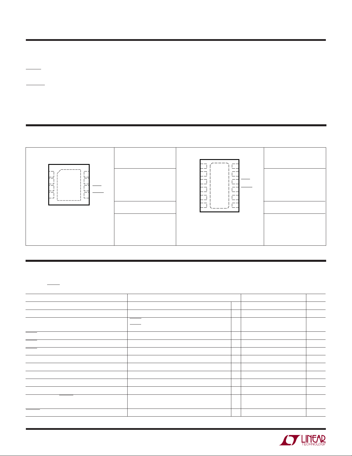
LT3473/LT3473A
Micropower 1A Boost
Converter with Schottky
and Output Disconnect
U
DESCRIPTIO
The LT®3473/LT3473A are micropower step-up DC/DC
converters with integrated Schottky diode and output
disconnect circuitry in low profile DFN packages. The
small package size, high level of integration and the use of
tiny SMT components yield a solution size of less than
2
50mm
25V at up to 80mA from a Li-Ion cell, while automatic Burst
Mode operation maintains efficiency at light load. An
auxiliary reference input (CTRL) allows the user to override the internal 1.25V feedback reference with any lower
value, allowing full control of the output voltage during
operation. A PGOOD pin sinks current when the output
voltage reaches 90% of final value.
The LT3473A includes two NPN transistors for generating
intermediate bias voltages from the output and is offered
in a 12-lead (4mm × 3mm) DFN package. The LT3473
does not include these NPNs and is offered in an 8-lead
(3mm × 3mm) package.
The rugged 36V switch and output disconnect circuitry
allow outputs up to 34V to be easily generated in a simple
boost topology.
, LTC and LT are registered trademarks of Linear Technology Corporation.
Burst Mode is a registered trademark of Linear Technology Corporation.
All other trademarks are the property of their respective owners.
. The internal 1A switch allows the device to deliver
TYPICAL APPLICATIO
PGOOD
CTRL
SW
V
IN
SHDN
LT3473
GND
V
3V TO 4.2V
4.7µF
IN
6.8µH
OUT
CAP
FB
U
2M
100k
2.2µF
0.47µF
3473 TA01a
V
OUT
25V
80mA
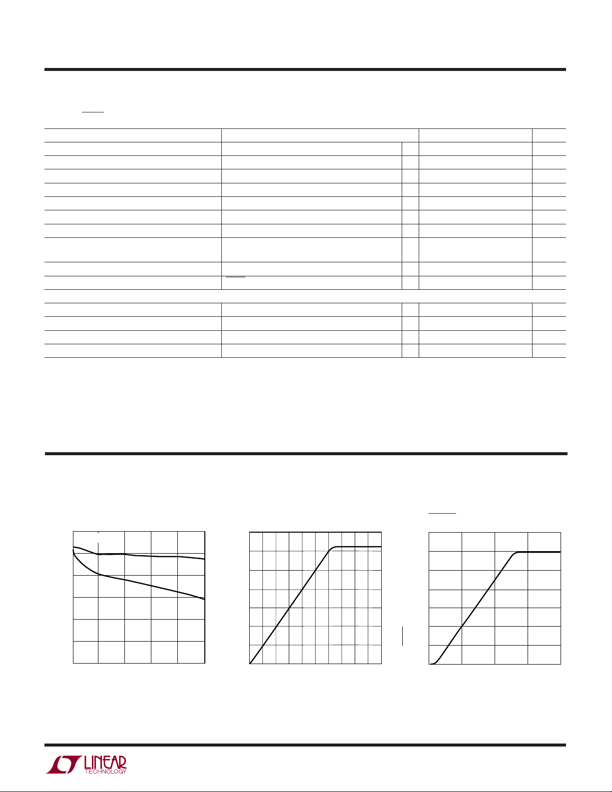
Conversion Efficiency and Power Loss vs Output Current
3473 TA01b
100
500
400
300
200
100
0
POWER LOSS (mW)
3473f
80
VIN = 3.6V
= 15V
V
OUT
75
70
65
EFFICIENCY (%)
60
55
0.1
1
OUTPUT CURRENT (mA)
10
1
LT3473/LT3473A
12
11
10
9
8
7
1
2
3
4
5
6
SW
V
IN
SHDN
PGOOD
CTRL
FB
CAP
OUT
NB1
NE1
NB2
NE2
TOP VIEW
13
DE PACKAGE
12-LEAD (4mm × 3mm) PLASTIC DFN
WWWU
ABSOLUTE AXI U RATI GS
(Note 1)
VIN Voltage ............................................................. 16V
SHDN Voltage .......................................................... 16V
SW Voltage ............................................................. 36V
PGOOD Voltage ...................................................... 36V
CAP Voltage ............................................................ 36V
OUT Voltage ........................................................... 36V
FB Voltage .............................................................. 10V
UU
W
PACKAGE/ORDER I FOR ATIO
TOP VIEW
1CAP
OUT
2
CTRL
3
FB
4
8-LEAD (3mm × 3mm) PLASTIC DFN
T
JMAX
EXPOSED PAD (PIN 9) IS GND
MUST BE SOLDERED TO PCB (NOTE 3)
9
DD PACKAGE
= 125°C, θJA = 43°C/ W
8
7
6
5
SW
V
IN
SHDN
PGOOD
ORDER PART
NUMBER
LT3473EDD
DD PART MARKING
LBJJ
CTRL Voltage .......................................................... 10V
NB1, NB2 Voltage ................................................... 36V
NE1, NE2 Voltage ................................................... 36V
Maximum Junction Temperature ......................... 125°C
Operating Temperature Range (Note 2) .. – 40°C to 85°C
Storage Temperature Range ................ –65°C to 125°C
ORDER PART
NUMBER
LT3473AEDE
DE PART MARKING
3473A
T
= 125°C, θJA = 43°C/ W
JMAX
EXPOSED PAD (PIN 13) IS GND
MUST BE SOLDERED TO PCB (NOTE 3)
Consult LTC Marketing for parts specified with wider operating temperature ranges.
ELECTRICAL CHARACTERISTICS
The ● denotes specifications which apply over the full operating temperature range, otherwise specifications are TA = 25°C.
VIN = 3V, SHDN = 3V, CTRL = 2V, unless otherwise specified.
PARAMETER CONDITIONS MIN TYP MAX UNITS
Minimum Operation Voltage 2.2 V
Maximum Operation Voltage 16 V
Supply Current SHDN = 3V, Not Switching 100 µA
SHDN Voltage to Enable Chip ● 1.4 V
SHDN Voltage to Disable Chip ● 0.2 V
SHDN Pin Bias Current 2 µA
FB Voltage ● 1.235 1.25 1.26 V
FB Voltage Line Regulation 3V < VIN < 16V 0.01 %/V
FB Pin Bias Current FB = 1.27V 20 nA
CTRL to FB Offset CTRL = 0.5V 5 20 mV
CTRL Pin Bias Current CTRL = 1V 50 nA
FB Threshold for PGOOD CTRL = 2V 1.15 V
PGOOD Current Capacity ● 100 µA
2
SHDN = 0V 0.1 1 µA
CTRL = 0.5V 0.40 V
3473f
LT3473/LT3473A
CTRL VOLTAGE (V)
0
1.0
1.2
1.4
2
3473 G03
0.8
0.6
0.5 1 1.5
0.4
0.2
0
PGOOD THRESHOLD VOLTAGE (V)
ELECTRICAL CHARACTERISTICS
The ● denotes specifications which apply over the full operating temperature range, otherwise specifications are TA = 25°C.
= 3V, SHDN = 3V, CTRL = 2V, unless otherwise specified.
V
IN
PARAMETER CONDITIONS MIN TYP MAX UNITS
Switching Frequency 0.9 1.2 1.4 MHz
Maximum Duty Cycle ● 88 92 %
Switch Current Limit ● 1.2 A
Switch V
CESAT
Switch Leakage Current VSW = 5V 0.1 5 µA
Schottky Forward Drop ID = 100mA 0.45 V
Schottky Leakage Current CAP = 36V, SW = 0V 4 µA
Disconnect PNP Voltage Drop I
Disconnect PNP Quiescent Current CAP = 20V 1.2 µA
Disconnect PNP Leakage Current SHDN = OUT = 0V, CAP = 20V 0.01 0.1 µA
LTC3473A Only
NPN1 Voltage Drop INE1 = 1mA 0.8 V
NPN1 Beta INE1 = 1mA 60
NPN2 Voltage Drop INE2 = 1mA 0.8 V
NPN2 Beta INE2 = 1mA 60
ISW = 100mA 45 mV
= 100µA, CAP = 20V 80 mV
OUT
= 50mA, CAP = 20V 250 mV
I
OUT
Note 1: Absolute Maximum Ratings are those values beyond which the life
of a device may be impaired.
Note 2: The LT3473EDD and LT3473AEDE are guaranteed to meet
performance specifications from 0°C to 70°C. Specifications over the
–40°C to 85°C operating temperature range are assured by design,
characterization and correlation with statistical process controls.
UW
TYPICAL PERFOR A CE CHARACTERISTICS
Load Regulation (Feedback Taken
from CAP)
20.20
VIN = 3.6V
20.00
19.80
19.60
VOLTAGE (V)
19.40
19.20
19.00
0
CAP
OUT
20 40 60 80
LOAD CURRENT (mA)
100
3473 G01
Feedback Voltage PGOOD Threshold Voltage
1.4
1.2
1.0
0.8
0.6
0.4
FEEDBACK VOLTAGE (V)
0.2
0
0
0.2
0.6
0.8
0.4
CTRL VOLTAGE (V)
Note 3: Failure to correctly solder the Exposed Pad of the package to the
PC board will result in a thermal resistance much higher than 40°C.
TA = 25°C unless otherwise noted.
1
1.2 1.6
1.4
1.8
3473 G02
2
3473f
3
LT3473/LT3473A
UW
TYPICAL PERFOR A CE CHARACTERISTICS
Sleep Mode Quiescent Current
Sleep Mode Quiescent Current
105
SHDN = 3V
= 3V
V
IN
100
(Not Switching)
102
100
98
96
SHDN = 3V
TA = 25°C unless otherwise noted.
SHDN Pin Current
2.5
SHDN = 3V
= 3V
V
IN
2.0
1.5
95
SLEEP MODE QUIESCENT CURRENT (µA)
90
–50
Switch V
450
400
350
300
250
200
150
100
50
SWITCH SATURATION VOLTAGE (mV)
0
0
050
TEMPERATURE (°C)
CE(SAT)
400
200
SWITCH CURRENT (mA)
600 1200
800
1000
3473 G04
3473 G07
100
94
92
90
SLEEP MODE QUIESCENT CURRENT (µA)
88
0
48
214
INPUT VOLTAGE, VIN (V)
SHDN = 1.5V
610 16
12
3473 G5
1.0
SHDN PIN CURRENT (µA)
0.5
0
–50
0
TEMPERATURE (°C)
Switch Saturation Voltage Schottky I-V Characteristic
50
= 100mA
I
SW
49
48
47
46
45
44
43
SWITCH SATURATION VOLTAGE (mV)
42
–50
050
TEMPERATURE (°C)
100
3473 G08
1000
900
800
700
600
500
400
300
200
SCHOTTKY FORWARD CURRENT (mA)
100
0
200
0
400
SCHOTTKY FORWARD DROP (mV)
600
50
800
100
3473 G06
1000
3473 G09
Schottky Forward Voltage
550
ID = 100mA
500
450
400
350
SCHOTTKY FORWARD VOLTAGE (mV)
300
–50
0
TEMPERATURE (°C)
4
Output Disconnect Voltage Drop
400
350
300
250
200
150
VOLTAGE DROP (mV)
100
50
50
100
3473 G10
0
20 40 60 100
0
COLLECTOR CURRENT (mA)
90°C
25°C
–45°C
80
3473 G11
Switching Frequency
1.4
1.2
1.0
0.8
0.6
0.4
SWITCHING FREQUENCY (MHz)
0.2
0
0
510
INPUT VOLTAGE, VIN (V)
15
3473 G12
3473f

UW
TYPICAL PERFOR A CE CHARACTERISTICS
SHDN Voltage to Turn-On
Disconnect PNP Quiescent Current
1.4
1.2
1.0
0.8
0.6
0.4
0.2
DISCONNECT PNP QUIESCENT CURRENT (µA)
0
0
10 20
535
15 25 40
CAP VOLTAGE (V)
30
3473 G13
Disconnect PNP
0.9
0.8
0.7
0.6
0.5
0.4
0.3
SHDN VOLTAGE (V)
0.2
0.1
0
0
20 60
40
OUTPUT CURRENT (mA)
80
LT3473/LT3473A
TA = 25°C unless otherwise noted.
3473 G14
100
Auxiliary NPN V
1.00
0.95
0.90
0.85
0.80
(V)
BE
0.75
0.70
NPN V
0.65
0.60
0.55
0.50
–50
BE
I
E
= 100µA
I
E
0
TEMPERATURE (°C)
= 1mA
50
100
3473 G15
U
PI FU CTIO S
UU
(LT3473/LT3473A)
CAP (Pin 1/Pin 1): Internal Output Voltage. This pin is the
Schottky cathode and disconnect PNP emitter. Connect
output capacitor here.
OUT (Pin 2/Pin 2): Output of Disconnect Circuit. Bypass
this pin with capacitor to ground.
CTRL (Pin 3/Pin 8): External Reference Pin. This pin sets
the FB voltage externally between 0V and 1.25V. Tie this
pin 1.5V or higher to use the internal 1.25V reference.
FB (Pin 4/Pin 7): Feedback Pin. Pin voltage is regulated to
1.25V if internal reference is used or to the CTRL pin
voltage if the CTRL pin voltage is between 0V and 1.25V.
Connect the feedback resistor divider to this pin. The
output voltage is regulated to:
R
2
VV
=+
OUT REF
⎛
•
⎜
⎝
⎞
1
⎟
⎠
R
1
PGOOD (Pin 5/Pin 9): Power Good Output. Open collector
logic output that starts to sink current when FB reaches
within 100mV of the reference voltage.
SHDN (Pin 6/Pin 10): Shutdown Pin. Connect to 1.4V or
higher to enable device; 0.2V or less to disable device. Also
functions as soft-start. Use RC filter as shown in Figure 4.
VIN (Pin 7/Pin 11): Input Supply Pin. Must be locally
bypassed with a X5R or X7R type ceramic capacitor.
SW (Pin 8/Pin 12): Switch Pin. Connect inductor here.
Minimize the metal trace area connected to the pin to
minimize EMI.
Exposed Pad (Pin 9/Pin 13): Ground. Solder directly to
PCB ground plane through multiple vias under the package for optimum thermal performance.
LT3473A Only
NB1 (Pin 3): NPN1 Base.
NE1 (Pin 4): NPN1 Emitter.
NB2 (Pin 5): NPN2 Base.
NE2 (Pin 6): NPN2 Emitter.
3473f
5

LT3473/LT3473A
BLOCK DIAGRA
W
4
3
5
9
FB
CTRL
100mV
PGOOD
GND
7
V
ERROR
AMPLIFIER
–
+
g
m
+
V
+
––
+
A4
REF
1.25V
IN
–
+
Q5
6
SHDN
V
C
+
BTH
–
POWER SECTION
A2
COMPARATOR
A1
ENABLE
R
Q
S
DRIVER
8
SW
Q1
PNP
DRIVER
CAP
1
Q2
OUT
2
–
Σ
RAMP
GENERATOR
1.2MHz
OSCILLATOR
A3
+
3437 F01
7
8
9
13
FB
CTRL
100mV
PGOOD
GND
Figure 1. LT3473 Block Diagram
12
SW
PNP
DRIVER
Q1
–
CAP
1
Q2
OUT
2
NB1
Q3
Q4
NE1
NB2
NE2
3
4
5
6
+
SHDN
IN
V
C
BTH
POWER SECTION
A2
COMPARATOR
10
+
–
OSCILLATOR
A1
R
1.2MHz
ENABLE
Q
S
DRIVER
A3
11
ERROR
AMPLIFIER
–
+
g
m
+
V
+
––
+
A4
REF
1.25V
V
–
+
Q5
Σ
RAMP
GENERATOR
6
3437 F02
Figure 2. LT3473A Block Diagram
3473f

WUUU
V
OUT
200mV/DIV
V
IN
= 3.6V
V
OUT
= 20V
500µs/DIV
3473 AI03
I
L
200mA/DIV
11mA
1mA
I
LOAD
APPLICATIO S I FOR ATIO
LT3473/LT3473A
Operation
The LT3473 combines a current mode, fixed frequency
PWM architecture with Burst Mode micropower operation
to maintain high efficiency at light loads. Operation can
best be understood by referring to the Block Diagram.
The reference of the part is determined by the lower of the
internal 1.25V bandgap reference and the voltage at the
CTRL pin. The error amplifier compares voltage at the FB
pin with the reference and generates an error signal V
When V
is below the Burst Mode threshold voltage, BTH,
C
.
C
the hysteretic comparator, A1, shuts off the power section
leaving only the low power circuitry running. Total current
consumption in this state is minimized. As output loading
Switching Waveforms Switching Waveforms Transient Response
200mA/DIV
V
10V/DIV
SW
I
L
200mA/DIV
V
10V/DIV
SW
I
L
causes the FB voltage to decrease, VC increases causing A1
to enable the power section circuitry. The chip starts switching. If the load is light, the output voltage (and FB voltage)
will increase until A1 turns off the power section. The output
voltage starts to fall again. This cycle repeats and generates low frequency ripple at the output. This Burst Mode
operation keeps the output regulated and reduces average
current into the IC, resulting in high efficiency at light load.
If the output load increases sufficiently, A1’s output remains
high, resulting in continuous operation.
At the start of each oscillator cycle, the SR latch is set,
turning on the power switch Q1. A voltage proportional to
the switch current is added to a stabilizing ramp and the
500mV/DIV
500mA/DIV
I
LOAD
V
OUT
51mA
1mA
I
L
V
V
I
LOAD
= 3.6V
IN
OUT
= 20V
= 50mA
0.5µs/DIV
3473 AI01
V
IN
V
OUT
I
LOAD
= 3.6V
= 20V
= 8mA
Transient Response Transient Response
V
OUT
500mV/DIV
I
L
500mA/DIV
55mA
I
LOAD
5mA
V
V
= 3.6V
IN
OUT
= 20V
V
V
= 3.6V
IN
OUT
= 20V
500µs/DIV
3473 AI04
0.5µs/DIV
Transient Response
500µs/DIV
3473 AI02
3473 AI05
V
500mV/DIV
500mA/DIV
75mA
I
LOAD
25mA
OUT
I
L
= 3.6V
V
IN
= 20V
V
OUT
Shutdown Waveforms Start-Up Waveforms
V
10V/DIV
0.5V/DIV
OUT
CAP
SHDN
5V/DIV
V
V
I
LOAD
= 3.6V
IN
OUT
= 20V
= 60mA
100µs/DIV
3473 AI07
V
OUT
10V/DIV
500mA/DIV
SHDN
2V/DIV
IL
= 3.6V
V
IN
= 20V
V
OUT
= 30mA
I
LOAD
SHDN 20k, 100nF
500µs/DIV
3473 AI08
200µs/DIV
3473 AI06
3473f
7

LT3473/LT3473A
WUUU
APPLICATIO S I FOR ATIO
resulting sum is fed into the positive terminal of the PWM
comparator A2. When this voltage exceeds the level of the
error signal V
switch Q1. The error amplifier sets the peak current level
to keep the output in regulation. If the error amplifier’s
output increases, more current is delivered to the output;
if it decreases, less current is delivered.
The LT3473 includes an internal power Schottky diode and
a PNP transistor, Q2, for output disconnect. Q2 disconnects the load from the input during shutdown. The part
also has a power good indication pin, PGOOD. When the
FB voltage reaches within 100mV of the reference voltage,
the comparator A4 turns on Q5, sinking current from
PGOOD pin.
The LT3473 has thermal shutdown feature with threshold
at about 145°C.
Inductor Selection
A 6.8µH inductor is recommended for the LT3473. The
minimum inductor size that may be used in a given application depends on required efficiency and output current.
, the SR latch is reset, turning off the power
C
80
VIN = 3.6V
= 20V
V
OUT
75
70
65
EFFICIENCY (%)
60
55
Figure 3. Efficiency Comparison of Different Inductors
20
0
TOKO A915AY-6R8M
SUMIDA CDRH4D28-6R8
SUMIDA CDRH5D18-6R2
COILCRAFT ME3220-682
COILCRAFT MSS5131-682
60
40
LEAD CURRENT lO (mA)
80
100
3473 F03
Capacitor Selection
The small package of ceramic capacitors makes them
suitable for LT3473 applications. X5R and X7R types of
ceramic capacitors are recommended because they retain
their capacitance over wider voltage and temperature
ranges than other types such as Y5V or Z5U. A 4.7µF input
capacitor, a 0.47µF output capacitor and a 2.2µF capacitor
bypassing output disconnect PNP are sufficient for most
LT3473 applications.
Inductors with low core losses and small DCR (copper
wire resistance) at 1.2MHz are good choices for LT3473
applications. Some inductors in this category with small
size are listed in Table 1. The efficiency comparison of
different inductors is shown in Figure 3.
Table 1. Recommended Inductors
DCR CURRENT DIMENSION
PART (mΩ) RATING (A) (mm) MANUFACTURER
DO1605T-682 200 1.1 5.4 × 4.2 × 1.8 Coilcraft
ME3220-682 270 1.0 3.2 × 2.5 × 2.0 800-322-2645
MSS6122-682 100 1.45 6.1 × 6.1 × 2.2
MSS5131-682 60 1.05 5.1 × 5.1 × 3.1
LQH55DN6R8 74 2.0 5.7 × 5.0 × 4.7 Murata
CDRH5D18-6R2 71 1.4 5.7 × 5.7 × 2.0 Sumida
CDRH4D28-6R8 81 1.12 4.7 × 4.7 × 3.0 847-956-0666
CDRH5D28-6R2 33 1.8 5.7 × 5.7 × 3.0
CRD53-4R7 74 1.68 6.0 × 5.2 × 3.2
A918CY-6R2M 62 1.49 6.0 × 6.0 × 2.0 Toko
(TYPE D62LCB) 408-432-8281
A915AY-6R8M 68 1.51 5.0 × 5.0 × 3.0
(TYPE D53LC)
Table 2. Recommended Ceramic Capacitor Manufacturers
MANUFACTURER TELEPHONE URL
Taiyo Yuden 408-573-4150 www.t-yuden.com
AVX 843-448-9411 www.avxcorp.com
Murata 814-237-1431 www.murata.com
Kemet 408-986-0424 www.kemet.com
www.coilcraft.com
814-237-1431
www.murata.com
www.sumida.com
www.tokoam.com
3473f
8

VV
R
R
INT REF
=+
⎛
⎝
⎜
⎞
⎠
⎟
•1
2
1
WUUU
SHDN
100nF
ON/OFF
3473 F04
20k
LT3473
APPLICATIO S I FOR ATIO
LT3473/LT3473A
Inrush Current
The LT3473 has an integrated Schottky power diode.
When supply voltage is abruptly applied to the V
while the output capacitor is discharged, the voltage
difference between V
flowing from the input through the inductor and the
internal Schottky diode to charge the output capacitor at
the CAP pin. The maximum current the LT3473’s Schottky
can sustain is 2A. The selection of inductor and capacitor
values should ensure that the peak inrush current is less
than 2A. Peak inrush current can be calculated as follows:
V
I
=
P
r
=
α
=
ω
where L is the inductance, r is the resistance of the
inductor and C is the output capacitance. For a low DCR
inductor, which is usually the case for this application, the
peak inrush current can be simplified as follows:
I
=
P
A large abrupt voltage step at VIN and/or a large capacitor
at the CAP pin generate larger inrush current. Table 3 gives
inrush peak currents for some component selections. An
inductor with low saturation current could generate very
large inrush current. For this case, inrush current should
be measured to ensure safe operation. Note that inrush
current is not a concern if the input voltage rises slowly.
Table 3. Inrush Peak Current
VIN (V) R (Ω)L (µH) C (µF) IP (A)
5 0.05 6.8 0.47 0.86
10 0.05 6.8 0.47 1.83
3.6 0.05 6.8 0.47 0.58
3.6 0.05 4.7 0.47 0.67
–.
IN
•
L
15
+
.
2
•
L
1
•
LC
V
IN
and CAP generates inrush current
IN
06
ω
–
–.
L
•
⎛
• exp – • arctan • sin arctan
4
06
α
⎜
ω
⎝
r
2
•
L
⎛
• exp – •
⎜
⎝
αωπ
⎞
ω
⎛
⎞
⎜
⎟
⎟
⎝
⎠
α
⎠
⎞
⎟
⎠
2ω
Setting the Output Voltages
The LT3473 has both an internal 1.25V reference and an
IN
pin
external reference input. This allows the user to select
between using the built-in reference and supplying an
external reference voltage. The voltage at the CTRL pin can
be adjusted while the device is operating to alter the output
voltage for purposes such as display dimming or contrast
adjustment. To use the internal 1.25V reference, the CTRL
pin must be held higher than 1.5V. When the CTRL pin is
held between 0V and 1.2V, the LT3473 will regulate the
output such that the FB pin voltage is equal to the CTRL pin
voltage.
⎛
⎜
⎝
⎞
ω
⎛
⎞
⎜
⎟
⎝
⎠
α
The CAP pin should be used as the feedback node. To set
⎟
⎠
the output voltage, select the values of R1 and R2 according to the following equation.
where V
V
= V
REF
= 1.25V if the internal reference is used, or
REF
CTRL
if V
is between 0V and 1.2V.
CTRL
To maintain output voltage accuracy, 1% resistors are
recommended.
Soft-Start
The SHDN pin also functions as soft-start. Use an RC filter
at the SHDN pin to limit the start-up current. The small bias
current of the SHDN pin allows using a small capacitor for
a large RC time constant.
Figure 4. Soft-Start Circuitry
Output Disconnect Considerations
The LT3473 has an output disconnect PNP that isolates
the load from the input during shutdown. The drive circuit
maintains the PNP at the edge of saturation, adaptively
according to the load, thus yielding the best compromise
between V
and quiescent current to minimize power
CESAT
loss. To remain stable, it requires a bypass capacitor
connected between the OUT pin and the CAP pin or
3473f
9

LT3473/LT3473A
WUUU
APPLICATIO S I FOR ATIO
between the OUT pin and ground. A ceramic capacitor with
a value of 1µF is a good choice. The voltage drop (PNP
V
) can be accounted for by setting the output voltage
CESAT
according to the following formula:
R
2
VVV V
==+
OUT INT CESAT REF CESAT
–•–1
⎛
⎜
⎝
⎞
V
⎟
⎠
R
1
Auxiliary NPN Devices (LT3473A Only)
The LT3473A has two auxiliary NPNs as shown in the
Block Diagram that can provide intermediate outputs less
than OUT. The collectors of the NPNs are connected to the
OUT pin internally. Each NPN can dissipate 100mW safely
and has a minimum beta of 60. A resistor string can be
OUT
2
R
EXT1
NB1
3
4
NE1
6
NE2
Figure 5. Auxiliary NPN Transistors in LT3473A. R
and R
Set Intermediate Voltage at NE1 and NE2
EXT3
R
EXT2
NB2
5
R
EXT3
3473 F05
, R
EXT1
EXT2
connected to the two bases as shown in Figure 5 to
generate buffered voltage at the emitters. When sourcing
high current at low voltage, keep in mind that the NPNs
will be dissipating a fair amount of power, which must be
supplied by the DC/DC converter.
Thermal Shutdown
The LT3473 has thermal shutdown circuitry that shuts down
the part when the junction temperature reaches approximately 145°C to protect the part from abnormal operation
with high power dissipation, such as an output short circuit or excessive power dissipation in the auxiliary NPNs.
The part will turn back on when the junction cools down to
approximately 125°C. If the abnormal condition remains,
the part will turn on and off while maintaining the junction
temperature within the window between 125°C and 145°C.
Board Layout Consideration
As with all switching regulators, careful attention must be
paid to the PCB board layout and component placement.
To maximize efficiency, switch rise and fall times are made
as short as possible. To prevent electromagnetic interference (EMI) problems, proper layout of the high frequency
switching path is essential. The voltage signal of the SW
pin has sharp rise and fall edges. Minimize the length and
area of all traces connected to the SW pin and always use
a ground plane under the switching regulator to minimize
interplane coupling. Recommended component placement is shown in Figure 6.
10
OUT
1
2
3
4
5
6
12
11
10
13
9
8
7
3473 F06a
OUT
1
2
3
4
8
7
9
6
5
3473 F06b
Figure 6. Recommended Component Placement
3473f

PACKAGE DESCRIPTIO
U
DD Package
8-Lead Plastic DFN (3mm × 3mm)
(Reference LTC DWG # 05-08-1698)
0.675 ±0.05
LT3473/LT3473A
R = 0.115
TYP
0.38 ± 0.10
85
3.5 ±0.05
1.65 ±0.05
(2 SIDES)2.15 ±0.05
PACKAGE
OUTLINE
0.25 ± 0.05
RECOMMENDED SOLDER PAD PITCH AND DIMENSIONS
NOTE:
1. DRAWING TO BE MADE A JEDEC PACKAGE OUTLINE M0-229 VARIATION OF (WEED-1)
2. DRAWING NOT TO SCALE
3. ALL DIMENSIONS ARE IN MILLIMETERS
4. DIMENSIONS OF EXPOSED PAD ON BOTTOM OF PACKAGE DO NOT INCLUDE
MOLD FLASH. MOLD FLASH, IF PRESENT, SHALL NOT EXCEED 0.15mm ON ANY SIDE
5. EXPOSED PAD SHALL BE SOLDER PLATED
6. SHADED AREA IS ONLY A REFERENCE FOR PIN 1 LOCATION
ON TOP AND BOTTOM OF PACKAGE
2.38 ±0.05
(2 SIDES)
0.50
BSC
PIN 1
TOP MARK
(NOTE 6)
0.200 REF
DE Package
12-Lead Plastic DFN (4mm × 3mm)
(Reference LTC DWG # 05-08-1708)
4.00 ±0.10
(2 SIDES)
0.65 ±0.05
3.00 ±0.10
(4 SIDES)
0.75 ±0.05
1.65 ± 0.10
0.00 – 0.05
R = 0.20
(2 SIDES)
0.25 ± 0.05
BOTTOM VIEW—EXPOSED PAD
TYP
2.38 ±0.10
(2 SIDES)
R = 0.115
TYP
14
0.50 BSC
(DD8) DFN 1203
0.38 ± 0.10
127
3.50 ±0.05
1.70 ±0.05
(2 SIDES)2.20 ±0.05
PACKAGE
OUTLINE
0.25 ± 0.05
3.30 ±0.05
(2 SIDES)
RECOMMENDED SOLDER PAD PITCH AND DIMENSIONS
NOTE:
1. DRAWING PROPOSED TO BE A VARIATION OF VERSION
(WGED) IN JEDEC PACKAGE OUTLINE M0-229
2. DRAWING NOT TO SCALE
3. ALL DIMENSIONS ARE IN MILLIMETERS
4. DIMENSIONS OF EXPOSED PAD ON BOTTOM OF PACKAGE DO NOT INCLUDE
MOLD FLASH. MOLD FLASH, IF PRESENT, SHALL NOT EXCEED 0.15mm ON ANY SIDE
0.50
BSC
PIN 1
TOP MARK
(NOTE 6)
0.200 REF
Information furnished by Linear Technology Corporation is believed to be accurate and reliable.
However, no responsibility is assumed for its use. Linear Technology Corporation makes no representation that the interconnection of its circuits as described herein will not infringe on existing patent rights.
3.00 ±0.10
(2 SIDES)
0.75 ±0.05
5. EXPOSED PAD SHALL BE SOLDER PLATED
6. SHADED AREA IS ONLY A REFERENCE FOR PIN 1 LOCATION
ON THE TOP AND BOTTOM OF PACKAGE
1.70 ± 0.10
(2 SIDES)
0.00 – 0.05
0.25 ± 0.05
BOTTOM VIEW—EXPOSED PAD
3.30 ±0.10
(2 SIDES)
0.50
BSC
16
PIN 1
NOTCH
(UE12/DE12) DFN 0603
3473f
11

LT3473/LT3473A
TYPICAL APPLICATIO
U
OLED Bias
80
75
70
65
EFFICIENCY (%)
60
55
0
V
3V TO 4.2V
4.7µF
100k
PGOOD
IN
L1 6.8µH
20k
C
IN
100nF
: TAIYO YUDEN JMK107BJ475
C
IN
: TAIYO YUDEN GMK212BJ474
C
INT
: TAIYO YUDEN GMK325BJ225
C
OUT
L1: TOKO A915AY-6R8M (TYPE D53LC)
CTRL
SW
V
IN
SHDN
LT3473
GND
OUT
CAP
V
OUT
25V
C
80mA
OUT
2.2µF
2M
C
FB
100k
0.47µF
3473 TA02a
INT
RELATED PARTS
PART NUMBER DESCRIPTION COMMENTS
LT1613 550mA (ISW), 1.4MHz, High Efficiency Step-Up VIN: 0.9V to 10V, V
DC/DC Converter ThinSOT
LT1615/LT1615-1 300mA/80mA (ISW), High Efficiency Step-Up VIN: 1V to 15V, V
DC/DC Converter
LT1930/LT1930A 1A (ISW), 1.2MHz/2.2MHz, High Efficiency Step-Up VIN: 2.6V to 16V, V
DC/DC Converter ThinSOT Package
LT1935 2A (ISW), 1.2MHz, High Efficiency Step-Up VIN: 2.3V to 16V, V
DC/DC Converter with Integrated Soft-Start ThinSOT Package
LT1945 Dual Output, Boost/Inverter, 350mA (ISW), Constant VIN: 1.2V to 15V, V
Off-Time, High Efficiency Step-Up DC/DC Converter 10-Lead MS Package
LT1946/LT1946A 1.5A (ISW), 1.2MHz/2.7MHz, High Efficiency Step-Up VIN: 2.45V to 16V, V
DC/DC Converter
LTC®3436 3A (ISW), 1MHz, 34V Step-Up DC/DC Converter VIN: 3V to 25V, V
LT3461/LT3461A 300mA (ISW), 1.3MHz/3MHz High Efficiency Step-Up VIN: 2.5V to 16V, V
DC/DC Converter with Integrated Schottky Diode ThinSOT Package
LT3463/LT3463A Dual Output, Boost/Inverter, 250mA (ISW), Constant VIN: 2.3V to 15V, V
Off-Time, High Efficiency Step-Up DC/DC Converters
with Integrated Schottkys
LT3464 85mA (ISW), High Efficiency Step-Up DC/DC Converter VIN: 2.3V to 10V, V
with Integrated Schottky and PNP Disconnect ThinSOT Package
LT3467/LT3467A 1.1A (ISW), 1.3MHz/2.1MHz, High Efficiency Step-Up VIN: 2.4V to 16V, V
DC/DC Converter with Soft-Start ThinSOT Package
LT3471 Dual Output, Boost/Inverter, 1.3A (ISW), 1.2MHz, VIN: 2.4V to 16V, V
High Efficiency Boost-Inverting DC/DC Converter
LT3479 3A (ISW), 3.5MHz, 42V Step-Up DC/DC Converter VIN: 2.5V to 24V, V
ThinSOT is a trademark of Linear Technology Corporation.
TM
Package
OUT(MAX)
OUT(MAX)
TSSOP-16E Package
DFN, TSSOP-16E Packages
Efficiency
VIN = 3.6V
V
= 25V
OUT
V
= 20V
OUT
20
40
LOAD CURRENT IO (mA)
= 34V, IQ = 3mA, ISD < 1µA,
OUT(MAX)
= 34V, IQ = 20µA, ISD < 1µA, ThinSOT Package
= 34V, IQ = 4.2mA/5.5mA, ISD < 1µA,
OUT(MAX)
= 38V, IQ = 3mA, ISD < 1µA,
OUT(MAX)
= ±34V, IQ = 40µA, ISD < 1µA,
OUT(MAX)
= 34V, IQ = 3.2mA, ISD < 1µA, MS8 Package
OUT(MAX)
= 34V, IQ = 0.9mA, ISD < 6µA,
= 38V, IQ = 2.8mA, ISD < 1µA,
OUT(MAX)
= ±40V, IQ = 40µA, ISD < 1µA, DFN Package
OUT(MAX)
= 34V, IQ = 25µA, ISD < 1µA,
OUT(MAX)
= 40V, IQ = 1.2mA, ISD < 1µA,
OUT(MAX)
= ±40V, IQ = 2.5mA, ISD < 1µA, DFN Package
OUT(MAX)
= 40V, IQ = 5mA, ISD < 1µA,
OUT(MAX)
V
= 15V
OUT
60
80
100
3473 TA02b
12
Linear Technology Corporation
1630 McCarthy Blvd., Milpitas, CA 95035-7417
(408) 432-1900 ● FAX: (408) 434-0507
●
www.linear.com
3473f
LT/TP 0205 1K • PRINTED IN THE USA
© LINEAR TECHNOLOGY CORPORATION 2005
 Loading...