

advertisement
ThinSOT Micropower Buck Regulator Has Low Output Ripple
Design Note 373
Keith Szolusha
Introduction
High voltage monolithic step-down converters simplify
circuit design and save space by integrating the high-side
power switch into the device. In most cases, the switch is
an n-type transistor (NMOS or NPN) with a boot-strapped
drive stage, requiring an external boost diode and capacitor as well as the main catch diode, complicating the
applications circuit.
®
The LT
switch, catch diode and boost diode integrated in a tiny
ThinSOT
3470 is a 40V step-down converter with the power
TM
package. The boosted NPN power stage provides high voltage capability, high power density and high
switching speed without the cost and space of external
diodes.
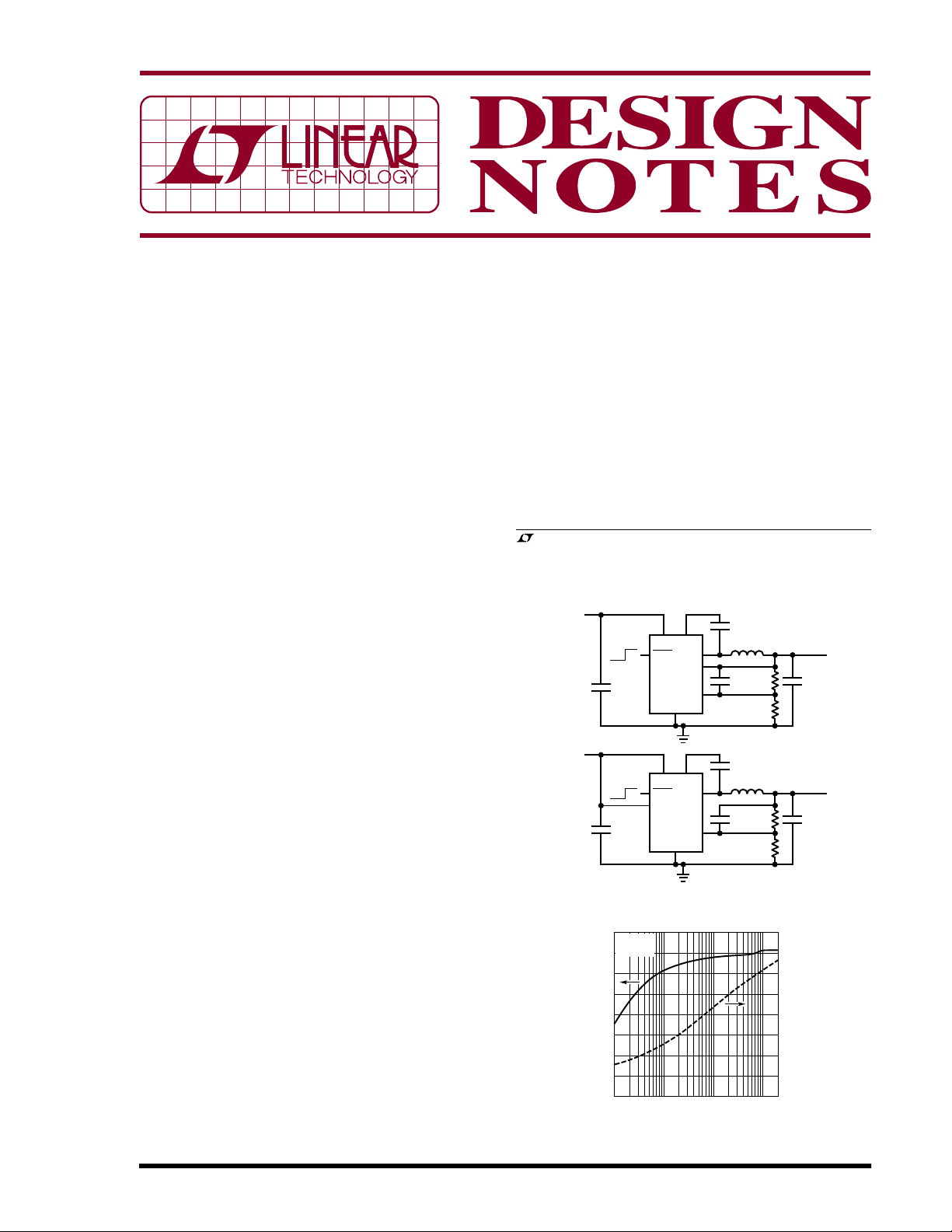
The LT3470 accepts an input voltage from 4V to 40V and
delivers up to 200mA to load. Micropower bias current
and Burst Mode
®
operation enable it to consume merely
26µA with no load and a 12V input. Hysteretic current
mode control and single-cycle bursts result in very low
output ripple and stable operation with small ceramic
capacitors. The combination of small circuit size, low
quiescent current and 40V input makes the LT3470 ideal
for automotive and industrial applications.
Current Mode Control
The LT3470 uses a hysteretic current control scheme in
conjunction with Burst Mode operation to provide low
output ripple and low quiescent current while using a tiny
inductor and ceramic capacitors. The switch turns on until
the current ramps up to the level of the top current comparator, then turns off and the inductor current ramps down
through the catch diode until the bottom current comparator trips and the minimum off-time has been met.
In continuous mode, the difference between the top and
bottom current comparator levels is about 150mA. Since
the switch only turns on when the catch diode current falls
below threshold, switching frequency decreases, keeping
switch current under control during start-up or shortcircuit conditions.
If the load is light, the IC alternates between micropower
and switching states to keep the output in regulation
(Figure 3a). Hysteretic mode allows the IC to provide
single switch-cycle bursts for the lowest possible lightload output voltage ripple (<20mV peak-to-peak from 12V
to 3.3V at zero load.) During continuous switching mode
(Figure 3b) at higher current levels, the output voltage
ripple is even smaller (<10mV peak-to-peak).
, LTC, LT and Burst Mode are registered trademarks and ThinSOT is a
trademark of Linear Technology Corporation. All other trademarks are the
property of their respective owners.
V
IN
4V TO 40V
5.5V
START-UP
4V TO 23V
OFF ON
V
IN
OFF ON
2.2µF
50V
CERAMIC
X5R
2.2µF
25V
CERAMIC
X5R
VINBOOST
SHDN
LT3470
GND
VINBOOST
SHDN
BIAS
LT3470
GND
V
BIAS
V
Figure 1. Typical 3.3V and 1.8V Output Applications
90
VIN = 12V
= 5V
V
OUT
80
70
60
50
40
EFFICIENCY (%)
30
20
10
0.1 10 100
1
LOAD CURRENT (mA)
Figure 2. Efficiency and Power Loss vs Load Current
0.22µF
6.3V
SW
FB
SW
FB
33µH
324k
22pF
1%
200k
1%
L: TOKO A003AS-270M=P3
0.22µF
25V
15µH
147k
22pF
1%
332k
1%
L: MURATA LQH32CN150K53
DN373 F02
22µF
6.3V
CERAMIC
X5R
22µF
6.3V
CERAMIC
X5R
DN373 F01
1000
100
POWER LOSS (mW)
10
1
0.1
V
OUT
3.3V
200mA
V
OUT
1.8V
200mA
10/05/373
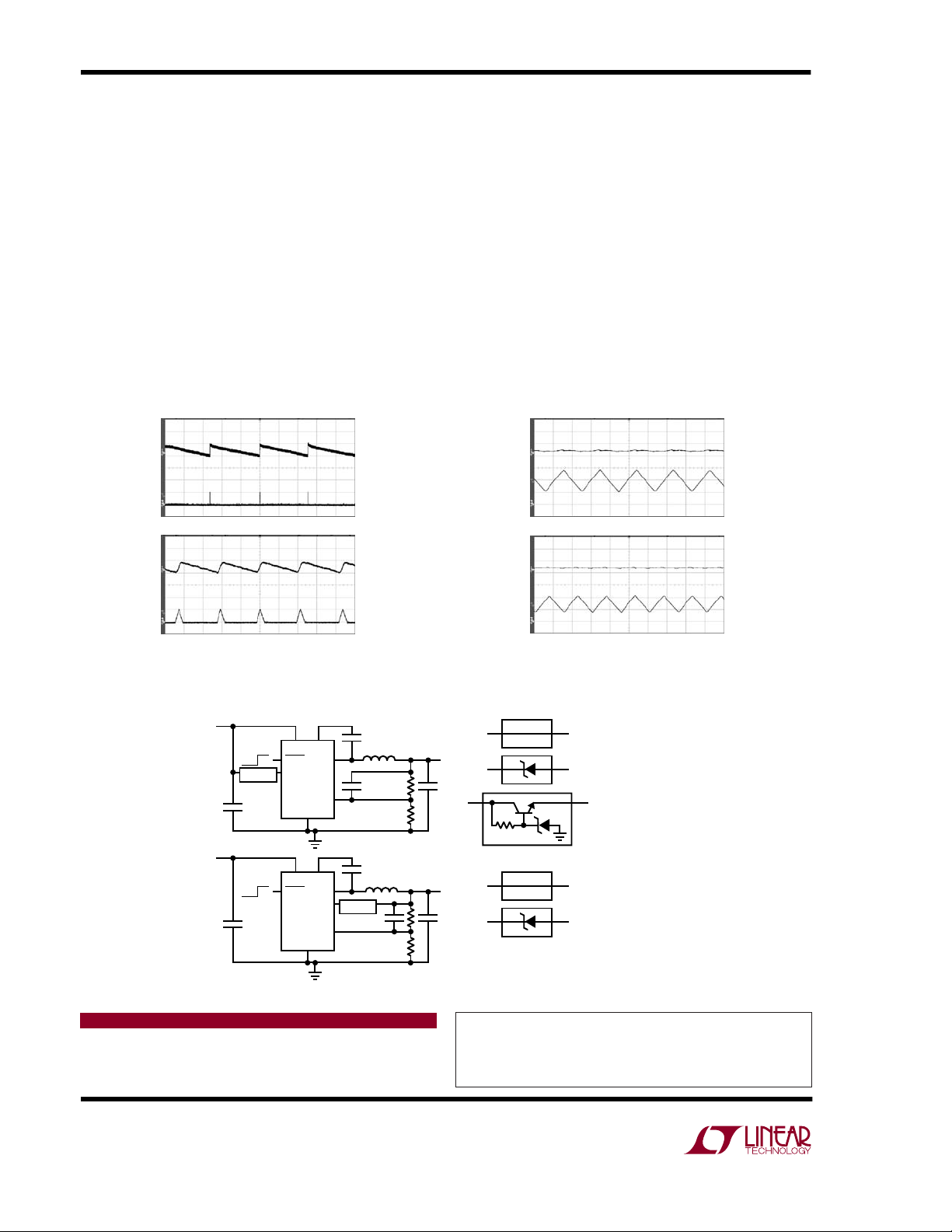
Design Flexibility with Integrated Boost Diode
A high side NPN power switch in a buck regulator design
needs a driver voltage that is at least a few volts higher than
the switch or input voltage. When there are no other high
voltage lines available, a bootstrapping method of providing several volts of boost to the IC is required. When there
is at least 2.5V on the output, the boost voltage can be most
efficiently derived from the output. If the output voltage is
too low, 1.8V for example, the boost voltage must be derived from the input.
Integration of the high side bootstrapping boost diode into
the IC does not limit boost diode flexibility. Boost diode flexibility such as the ability to connect to various sources and/
or the inclusion of a Zener blocking diode is needed for both
high and low output voltages with and without wide input
voltage ranges. The anode of the boost diode can be con-
NO LOAD
V
OUT
20mV/DIV
I
L
100mA/DIV
1ms/DIV
10mA LOAD
V
OUT
20mV/DIV
nected to different sources via the BIAS pin. In most cases,
this is a simple connection to either the input, when the
output voltage is below 2.5V, or the output, for output
voltages above 2.5V. Additional Zener diode voltage drop
in the boost diode path or a transistor bias supply as shown
in Figure 4 protects the IC from BOOST pin overvoltage
when there is a wide input voltage range.
Conclusion
The LT3470 is a wide input voltage range, hysteretic mode,
fully integrated monolithic 300mA step-down DC/DC converter. The onboard high side NPN power switch, Schottky boost diode, and Schottky catch diode combined with
the small ThinSOT package and high 40V input voltage
make this a simple and versatile IC to use for many stepdown applications with less than 200mA load current.
200mA LOAD
V
OUT
20mV/DIV
I
L
100mA/DIV
1µs/DIV
150mA LOAD
V
OUT
20mV/DIV
I
L
100mA/DIV
Figure 3. (3a) Burst Mode Operation—Single Pulse Burst Mode Operation Has Only 20mV
(3b) Continuous Operation—Extremely Low Output Voltage Ripple
Figure 4. BIAS and BOOST Pin Connection Variations Provide Input and Output Voltage Range Flexibility
Data Sheet Download
http://www.linear.com
I
L
100mA/DIV
VINBOOST
SHDN
LT3470
GND
VINBOOST
SHDN
LT3470
GND
V
V
BIAS
SW
SW
FB
FB
DN373 F03a
V
OUT
≥ 2.5V
DN373 F04
1µs/DIV
(3b)
V
IN
V
V
OUT
IN
V
IN
V
OUT
V
OUT
V
OUT
BIAS
DIRECT
V
BIAS
ZENER
V
BIAS
TRANSISTOR BIAS
V
BIAS
DIRECT
V
BIAS
ZENER
V
BOOST(MAX)
BOOST(MAX)
BOOST(MAX)
BOOST(MAX)
BOOST(MAX)
= VIN • 2
= VIN • 2 – V
= VIN + VZ – V
= VIN + V
= VIN + V
5µs/DIV
(3a)
V
IN
OFF ON
BIAS
V
< 2.5V
OUT
V
IN
OFF ON
OUT
OUT
Z
BE
– V
DN373 F03b
Ripple.
P-P
Z
For applications help,
call (408) 432-1900, Ext. 2759
Linear Technology Corporation
1630 McCarthy Blvd., Milpitas, CA 95035-7417
(408) 432-1900 ● FAX: (408) 434-0507 ● www.linear.com
dn373f LT/TP 1005 409K • PRINTED IN THE USA
© LINEAR TECHNOLOGY CORPORATION 2005
 Loading...