

Page 1
advertisement
Basic Flashlamp Illumination Circuitry for
Cellular Telephones/Cameras – Design Note 345
Jim Williams
Introduction
Next generation cellular telephones will include high quality photographic capability. Flashlamp-based lighting is
crucial for good photographic performance. A previous
full-length Linear Technology publication detailed flash
illumination issues and presented flash circuitry equipped
with “red-eye” reduction capability.
1,2
Some applications
do not require this feature; deleting it results in an
extremely simple and compact flashlamp solution.
Flashlamp Circuitry
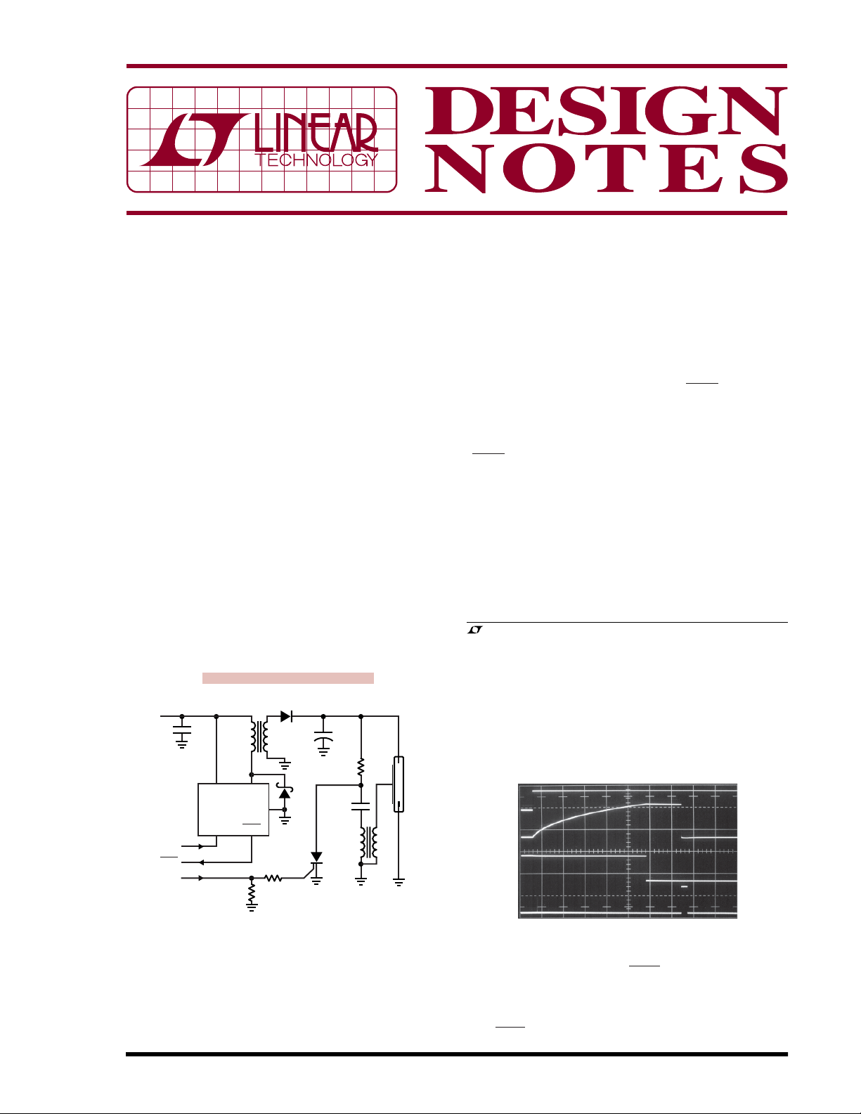
Figure 1’s circuit consists of a power converter, flashlamp,
storage capacitor and an SCR-based trigger. In operation
®
the LT
3468-1 charges C1 to a regulated 300V at about
80% efficiency. A “trigger” input turns the SCR on,
depositing C2’s charge into T2, producing a high voltage
trigger event at the flashlamp. This causes the lamp to
conduct high current from C1, resulting in an intense flash
of light. LT3468-1 associated waveforms, appearing in
DANGER! Lethal Potentials Present — Use Caution
FLASH STORAGE
D1
+V
3V TO 6V
IN
CHARGE
DONE
TRIGGER
4.7µF
V
IN
LT3468-1
CHARGE
T1
5
8
SW
GND
DONE
CAPACITOR
CHARGER
10k
CAPACITOR
4
1
1k
+
C1
13µF
330V
TRIGGER
D2
0.047µF
400V
C2
1
2
A
R1
1M
T
FLASHLAMP
C
T2
3
DN345 F01
Figure 2, include trace A, the “charge input,” going high.
This initiates T1 switching, causing C1 to ramp up (trace
B). When C1 arrives at the regulation point, switching
ceases and the resistively pulled-up “DONE” line drops
low (trace C), indicating C1’s charged state. The “TRIGGER” command (trace D), resulting in C1’s discharge via
the lamp, may occur any time (in this case ≈600ms) after
“DONE” goes low. Normally, regulation feedback would
be provided
by resistively dividing down the output
voltage. This approach is not acceptable because it would
require excessive switch cycling to offset the feedback
resistor’s constant power drain. While this action would
maintain regulation, it would also drain excessive power
from the primary source, presumably a battery. Regulation is instead obtained by monitoring T1’s flyback pulse
characteristic, which reflects T1’s secondary amplitude.
, LTC and LT are registered trademarks of Linear Technology Corporation.
Note 1. See LTC Application Note 95, “Simple Circuitry for
Cellular Telephone/Camera Flash Illuminaton” by Jim Williams
and Albert Wu, March 2004.
Note 2. “Red-eye” in a photograph is caused by the human
retina reflecting the light flash with a distinct red color. It is
eliminated by causing the eye’s iris to constrict in response to a
low intensity flash immediately preceding the main flash.
A = 5V/DIV
B = 200V/DIV
C = 5V/DIV
D = 5V/DIV
C1: RUBYCON 330FW13AK6325
D1: TOSHIBA DUAL DIODE 1SS306,
CONNECT DIODES IN SERIES
D2: PANASONIC MA2Z720
SCR: TOSHIBA S6A37
T1: TDK LDT565630T-002
T2: TOKYO COIL-BO-02
FLASHLAMP: PERKIN ELMER BGDC0007PKI5700
Figure 1. Complete Flashlamp Circuit Includes Capacitor
Charging Components, Flash Capacitor C1, Trigger (R1,
C2, T2, SCR) and Flashlamp. TRIGGER Command Biases
SCR, Ionizing Lamp via T2. Resultant C1 Discharge
Through Lamp Produces Light
09/04/345
400ms/DIV DN345 F02
Figure 2. Capacitor Charging Waveforms Include Charge
Input (Trace A), C1 (Trace B), DONE Output (Trace C) and
TRIGGER Input (Trace D). C1’s Charge Time depends Upon
Its Value and Charge Circuit Output Impedance. TRIGGER
Input, Widened for Figure Clarity, May Occur any Time
After DONE Goes Low
Page 2
The output voltage is set by T1’s turns ratio. This feature
permits tight capacitor voltage regulation, necessary to
ensure consistent flash intensity without exceeding lamp
energy or capacitor voltage ratings. Also, flashlamp energy is conveniently determined by the capacitor value
without any other circuit dependencies.
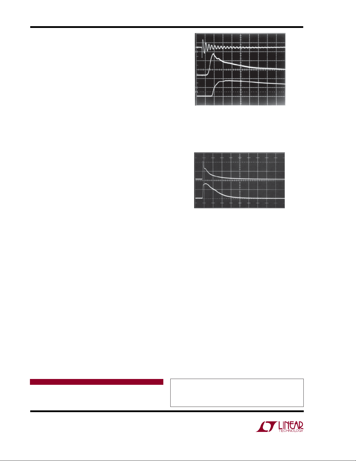
A = 2000V/DIV
B = 50A/DIV
Figure 3 shows high speed detail of the high voltage
trigger pulse (trace A), the flashlamp current (trace B)
and the light output (trace C).
Some amount of time is
required for the lamp to ionize and begin conduction after
triggering. Here, 3µs after the 4kV
trigger pulse,
P-P
flashlamp current begins its ascent to over 100A. The
current rises smoothly in 3.5µs to a well defined peak
before beginning its descent. The resultant light produced
rises more slowly, peaking in about 7µs before decaying.
Slowing the oscilloscope sweep permits capturing the
entire current and light events. Figure 4 shows that light
output (trace B) follows lamp current (trace A) profile,
although current peaking is more abrupt. Total event
duration is ≈200µs with most energy expended in the first
100µs.
Conclusion
The circuit presented constitutes a basic, but high performance, flash illumination solution. Its low power, small
size and few components suit cellular telephone/camera
applications where size and power drain are important. It
provides a practical, readily adaptable path to accessing
flashlamp-based illumination’s photographic advantages.
C = RELATIVE
LIGHT/DIV
5µs/DIV
DN345 F03
Figure 3. High Speed Detail of Trigger Pulse (Trace A),
Resultant Flashlamp Current (Trace B) and Relative Light
Output (Trace C). Current Exceeds 100A After Trigger Pulse
Ionizes Lamp
A = 50A/DIV
B = RELATIVE
LIGHT/DIV
50µs/DIV
DN345 F04
Figure 4. Photograph Captures Entire Current (Trace A)
and Light (Trace B) Events. Light Output Follows Current
Profile Although Peaking is Less Defined. Waveform
Leading Edges Enhanced for Figure Clarity
Data Sheet Download
http://www.linear.com
Linear Technology Corporation
1630 McCarthy Blvd., Milpitas, CA 95035-7417
(408) 432-1900 ● FAX: (408) 434-0507 ● www.linear.com
For applications help,
call (408) 432-1900, Ext. 2759
dn345f LT/TP 0904 305K • PRINTED IN THE USA
© LINEAR TECHNOLOGY CORPORATION 2004
 Loading...