

FEATURES
LT3468/LT3468-1/LT3468-2
Photoflash Capacitor
TM
Chargers in ThinSOT
U
DESCRIPTIO
■
Highly Integrated IC Reduces Solution Size
■
Uses Small Transformers:
5.8mm × 5.8mm × 3mm
■
Fast Photoflash Charge Times:
4.6s for LT3468 (0V to 320V, 100µF, V
5.7s for LT3468-2 (0V to 320V, 100µF, V
= 3.6V)
IN
= 3.6V)
IN
5.5s for LT3468-1 (0V to 320V, 50µF, VIN = 3.6V)
■
Controlled Input Current:
500mA (LT3468)
375mA (LT3468-2)
225mA (LT3468-1)
■
Supports Operation from Single Li-Ion Cell, or Any
Supply from 2.5V up to 16V
■
Adjustable Output Voltage
■
No Output Voltage Divider Needed
■
Charges Any Size Photoflash Capacitor
■
Low Profile (<1mm) SOT-23 Package
U
APPLICATIO S
■
Digital / Film Camera Flash
■
PDA / Cell Phone Flash
■
Emergency Strobe
The LT®3468/LT3468-1/LT3468-2 are highly integrated
ICs designed to charge photoflash capacitors in digital and
film cameras. A patented control technique* allows for the
use of extremely small transformers. Each device contains
an on-chip high voltage NPN power switch. Output voltage
detection* is completely contained within the device,
eliminating the need for any discrete zener diodes or
resistors. The output voltage can be adjusted by simply
changing the turns ratio of the transformer. The LT3468
has a primary current limit of 1.4A, the LT3468-2 has a 1A
limit, and the LT3468-1 has a 0.7A limit. These different
current limit levels result in well controlled input currents
of 500mA for the LT3468, 375mA for the LT3468-2 and
225mA for the LT3468-1. Aside from the differing current
limit, the three devices are otherwise equivalent.
The CHARGE pin gives full control of the part to the user.
Driving CHARGE low puts the part in shutdown. The DONE
pin indicates when the part has completed charging. The
LT3468 series of parts are available in tiny low profile
(1mm) SOT-23 packages.
, LTC and LT are registered trademarks of Linear Technology Corporation.
ThinSOT is a trademark of Linear Technology Corporation.
All other trademarks are the property of their respective owners.
*Protected by U.S. Patents, including 6518733.
U
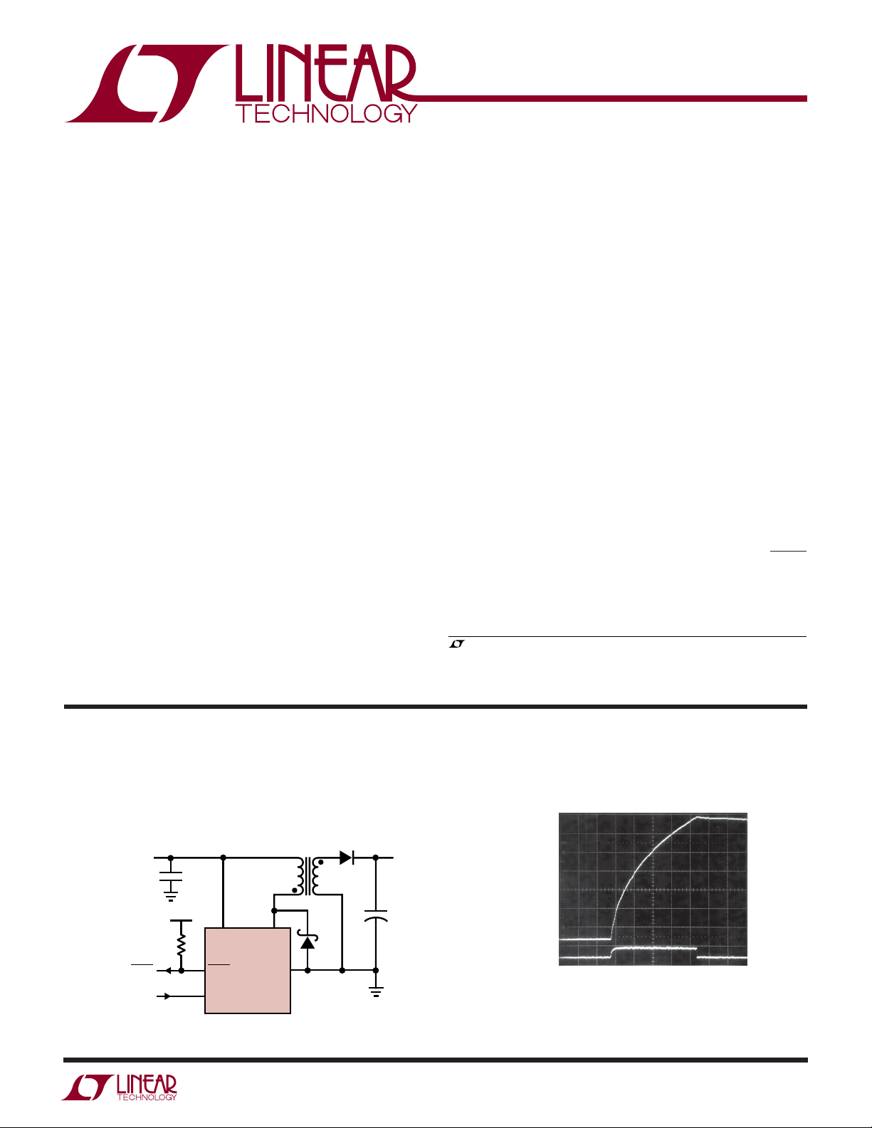
TYPICAL APPLICATIO
LT3468 Photoflash Charger Uses
High Efficiency 4mm Tall Transformer
DANGER HIGH VOLTAGE – OPERATION BY HIGH VOLTAGE
TRAINED PERSONNEL ONLY
V
IN
2.5V TO 8V
100k
DONE DONE
CHARGE
4.7µF
V
IN
CHARGE
LT3468
1:10.2
1
2
SW
GND
LT3468 Charging Waveform
VIN = 3.6V
= 100µF
C
OUT
4
5
320V
+
100µF
346812 TA01
V
OUT
50V/DIV
AVERAGE
INPUT
CURRENT
1A/DIV
1s/DIV
3468 G01
346812fa
1

LT3468/LT3468-1/LT3468-2
5 VIN
4 CHARGE
SW 1
TOP VIEW
S5 PACKAGE
5-LEAD PLASTIC TSOT-23
GND 2
DONE 3
ABSOLUTE AXI U RATI GS
(Note 1)
VIN Voltage .............................................................. 16V
SW Voltage ................................................ –0.4V to 50V
CHARGE Voltage...................................................... 10V
DONE Voltage .......................................................... 10V
Current into DONE Pin .......................................... ±1mA
Maximum Junction Temperature .......................... 125°C
Operating Temperature Range (Note 2) ...–40°C to 85°C
Storage Temperature Range ..................–65°C to 150°C
Lead Temperature (Soldering, 10 sec).................. 300°C
ELECTRICAL CHARACTERISTICS
temperature range, otherwise specifications are at TA = 25°C. VIN = 3V, V
are for the LT3468, LT3468-1 and LT3468-2 unless otherwise noted.
PARAMETER CONDITIONS MIN TYP MAX UNITS
Quiescent Current Not Switching 5 8 mA
Input Voltage Range ● 2.5 16 V
Switch Current Limit LT3468 (Note 3) 1.1 1.2 1.3 A
Switch V
V
OUT
V
OUT
DCM Comparator Trip Voltage Measured as V
CHARGE Pin Current V
Switch Leakage Current VIN = VSW = 5V, in Shutdown ● 0.01 1 µA
CHARGE Input Voltage High ● 1V
CHARGE Input Voltage Low ● 0.3 V
Minimum Charge Pin Low Time High→Low→High 20 µs
DONE Output Signal High 100kΩ from VIN to DONE 3 V
DONE Output Signal Low 33µA into DONE Pin 100 200 mV
DONE Leakage Current V
Note 1: Absolute Maximum Ratings are those values beyond which the life
of a device may be impaired.
Note 2: The LT3468E/LT3468E-1/LT3468E-2 are guaranteed to meet
performance specifications from 0°C to 70°C. Specifications over the
2
WW
W
U
UUW
PACKAGE/ORDER I FOR ATIO
ORDER PART
NUMBER
LT3468ES5
LT3468ES5-1
LT3468ES5-2
S5 PART
T
= 125°C
JMAX
= 150°C ON BOARD OVER
θ
JA
GROUND PLANE
θJC = 90°C/W
Consult LTC Marketing for parts specified with wider operating temperature ranges.
The ● denotes the specifications which apply over the full operating
= VIN unless otherwise noted. (Note 2) Specifications
CHARGE
V
= 0V 0 1 µA
CHARGE
LT3468-2 0.77 0.87 0.97 A
LT3468-1 0.45 0.55 0.65 A
CESAT
Comparator Trip Voltage Measured as V
Comparator Overdrive 300ns Pulse Width 200 400 mV
LT3468, I
LT3468-2, I
LT3468-1, I
CHARGE
V
CHARGE
DONE
= 1A 330 430 mV
SW
= 650mA 210 280 mV
SW
= 400mA 150 200 mV
SW
– V
SW
IN
– V
SW
IN
= 3V 15 40 µA
= 0V 0 0.1 µA
= 3V, DONE NPN Off 20 100 nA
–40°C to 85°C operating temperature range are assured by design,
characterization and correlation with statistical process.
Note 3: Specifications are for static test. Current limit in actual application
will be slightly higher.
● 31 31.5 32 V
● 10 36 80 mV
MARKING
LTAEC
LTAGQ
LTBCH
346812fa
LT3468/LT3468-1/LT3468-2
UW
TYPICAL PERFOR A CE CHARACTERISTICS
curves use the circuit of Figure 7 and LT3468-2 use the circuit of Figure 8 unless otherwise noted.
LT3468 curves use the circuit of Figure 6, LT3468-1
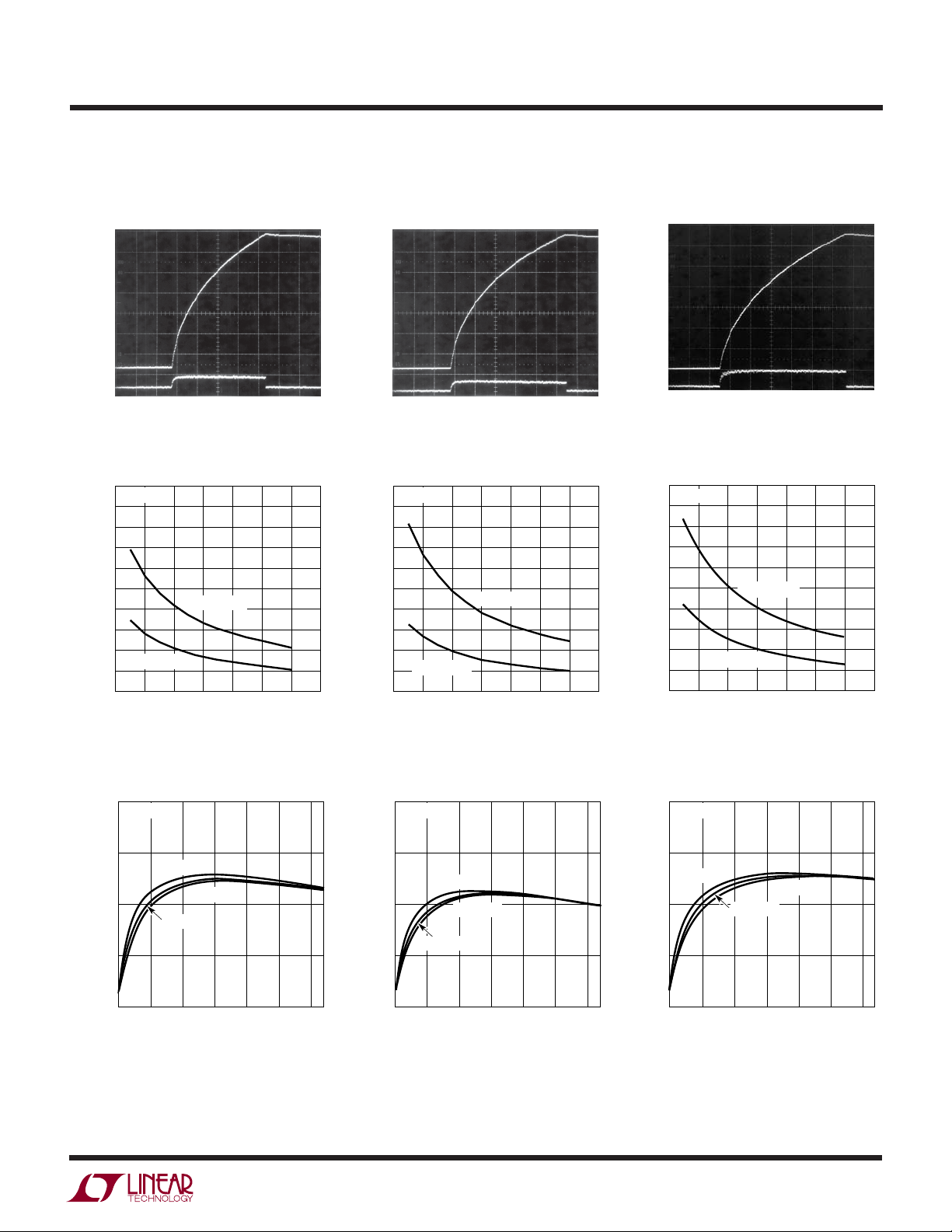
LT3468 Charging Waveform
VIN = 3.6V
= 100µF
C
OUT
V
OUT
50V/DIV
AVERAGE
INPUT
CURRENT
1A/DIV
1s/DIV
LT3468 Charge Time
10
TA = 25°C
9
8
7
6
5
4
CHARGE TIME (s)
3
2
C
OUT
1
0
23456789
= 50µF
C
OUT
= 100µF
VIN (V)
3468 G01
3468 G04
LT3468-1 Charging Waveform
VIN = 3.6V
= 50µF
C
OUT
V
OUT
50V/DIV
AVERAGE
INPUT
CURRENT
0.5A/DIV
1s/DIV
LT3468-1 Charge Time
10
TA = 25°C
9
8
7
6
5
4
CHARGE TIME (s)
3
2
C
1
OUT
0
23456789
= 20µF
C
OUT
VIN (V)
= 50µF
3468 G02
3468 G05
V
OUT
50V/DIV
AVERAGE
INPUT
CURRENT
0.5A/DIV
10
9
8
7
6
5
4
CHARGE TIME (s)
3
2
1
0
LT3468-2 Charging Waveform
VIN = 3.6V
C
= 100µF
OUT
1s/DIV
LT3468-2 Charge Time
TA = 25°C
C
= 100µF
OUT
C
= 50µF
OUT
6
5
2
4
3
VIN (V)
7
8
3468 G03
9
3468 G06
LT3468 Input Current LT3468-1 Input Current
800
TA = 25°C
600
400
200
AVERAGE INPUT CURRENT (mA)
0
VIN = 2.8V
VIN = 4.2V
VIN = 3.6V
0 50 100 150 200 250 300
V
(V)
OUT
3468 G07
400
TA = 25°C
300
VIN = 2.8V
200
100
AVERAGE INPUT CURRENT (mA)
0
0 50 100 150 200 250 300
VIN = 4.2V
VIN = 3.6V
LT3468-2 Input Current
600
TA = 25°C
450
VIN = 2.8V
300
150
AVERAGE INPUT CURRENT (mA)
0
V
(V)
OUT
3468 G08
0 50 100 150 200 250 300
VIN = 3.6V
V
OUT
VIN = 4.2V
(V)
3468 G09
346812fa
3
LT3468/LT3468-1/LT3468-2
TEMPERATURE (°C)
–40
I
LIM
(A)
1.00
0.96
0.92
0.88
0.84
0.80
0
40
60
34682 G18
–20
20
80
100
VIN = 3V
V
OUT
= 0V
UW
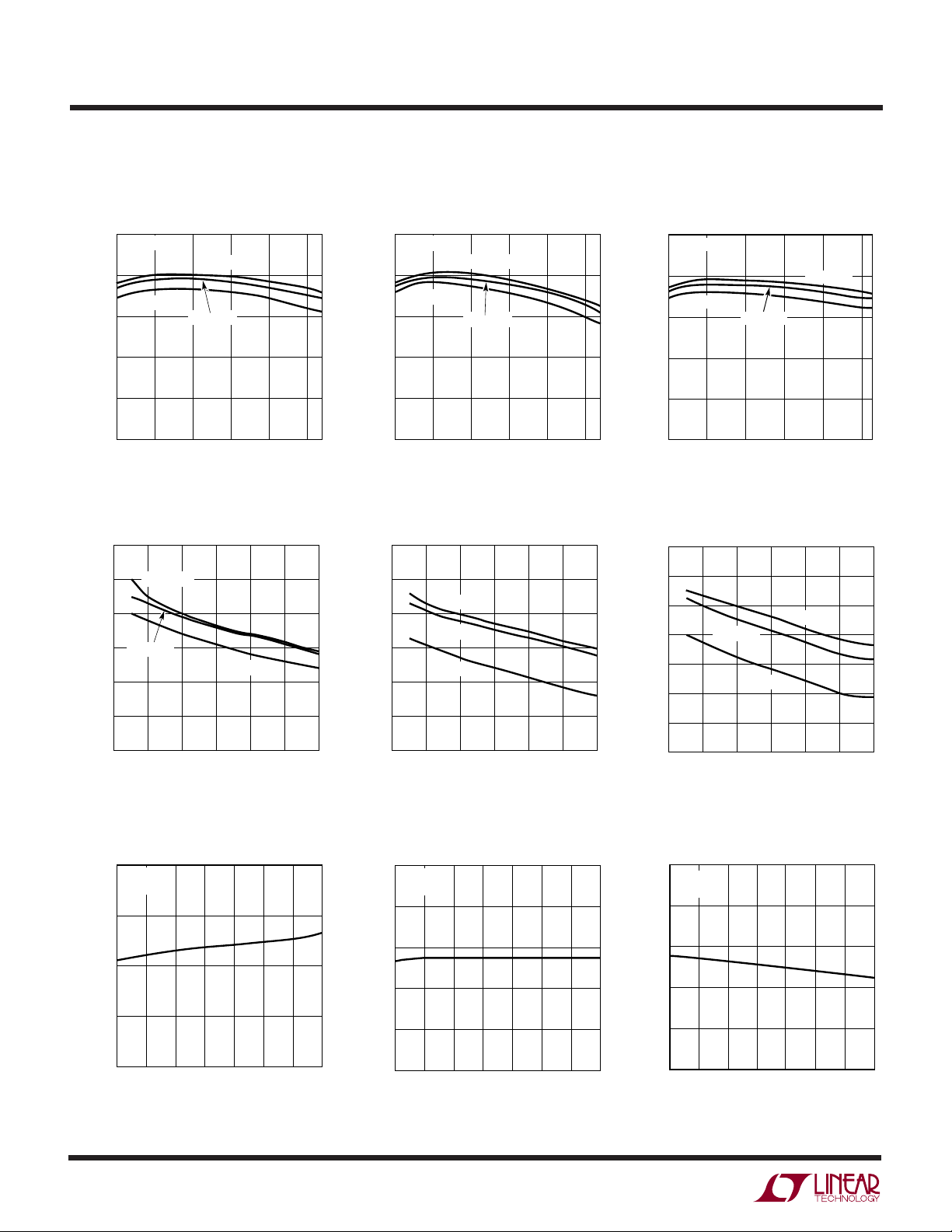
TYPICAL PERFOR A CE CHARACTERISTICS
curves use the circuit of Figure 7 and LT3468-2 use the circuit of Figure 8 unless otherwise noted.
LT3468 curves use the circuit of Figure 6, LT3468-1
LT3468 Efficiency LT3468-1 Efficiency
90
TA = 25°C
80
VIN = 2.8V
70
60
EFFICIENCY (%)
50
40
50 100 150 200 250 300
VIN = 4.2V
VIN = 3.6V
V
(V)
OUT
3468 G10
90
TA = 25°C
80
VIN = 2.8V
70
60
EFFICIENCY (%)
50
40
50 100 150 200 250 300
LT3468-1 Output VoltageLT3468 Output Voltage
(V)
OUT
V
324
323
322
321
320
319
TA = –40°C
TA = 25°C
TA = 85°C
(V)
OUT
V
324
323
322
321
320
319
TA = –40°C
TA = 25°C
TA = 85°C
VIN = 4.2V
VIN = 3.6V
V
OUT
(V)
3468 G11
LT3468-2 Efficiency
90
TA = 25°C
80
VIN = 2.8V
70
60
EFFICIENCY (%)
50
40
50
100
VIN = 3.6V
150
V
LT3468-2 Output Voltage
319
318
317
(V)
OUT
V
316
315
314
313
TA = 85°C
TA = –40°C
OUT
200
(V)
VIN = 4.2V
250
TA = 25°C
300
3468 G12
4
318
2345678
VIN (V)
LT3468 Switch Current Limit
1.5
VIN = 3V
= 0V
V
OUT
1.4
(A)
1.3
LIM
I
1.2
1.1
–40 –20 0 20 40 60 10080
TEMPERATURE (°C)
3468 G13
3468 G16
318
2345678
VIN (V)
LT3468-1 Switch Current Limit
0.700
VIN = 3V
= 0V
V
OUT
0.660
0.620
(A)
LIM
I
0.580
0.540
0.500
–40 –20 0 20 40 60 10080
TEMPERATURE (°C)
3468 G14
3468 G17
312
2
45678
3
VIN (V)
LT3468-2 Switch Current Limit
3468 G15
346812fa
LT3468/LT3468-1/LT3468-2
UW
TYPICAL PERFOR A CE CHARACTERISTICS
curves use the circuit of Figure 7 and LT3468-2 use the circuit of Figure 8 unless otherwise noted.
LT3468 curves use the circuit of Figure 6, LT3468-1
LT3468 Switching Waveform
VIN = 3.6V
= 100V
V
OUT
V
SW
10V/DIV
I
PRI
1A/DIV
1µs/DIV
LT3468 Switching Waveform
VIN = 3.6V
= 300V
V
OUT
V
SW
10V/DIV
I
PRI
1A/DIV
3468 G19
LT3468-1 Switching Waveform
VIN = 3.6V
V
= 100V
OUT
V
SW
10V/DIV
I
PRI
1A/DIV
1µs/DIV
LT3468-1 Switching Waveform
VIN = 3.6V
= 300V
V
OUT
V
SW
10V/DIV
I
PRI
1A/DIV
3468 G22
LT3468-2 Switching Waveform
VIN = 3.6V
= 100V
V
OUT
V
SW
10V/DIV
I
PRI
1A/DIV
1µs/DIV
LT3468-2 Switching Waveform
VIN = 3.6V
= 300V
V
OUT
V
SW
10V/DIV
I
PRI
1A/DIV
3468 G21
1µs/DIV
3468 G20
1µs/DIV
LT3468/LT3468-1/LT3468-2
Switch Breakdown Voltage
10
SW PIN IS RESISTIVE UNTIL BREAKDOWN
VOLTAGE DUE TO INTEGRATED
9
RESISTORS. THIS DOES NOT INCREASE
8
QUIESCENT CURRENT OF PART
7
6
5
4
3
SWITCH CURRENT (mA)
2
1
0
0 102030405060708090100
SWITCH VOLTAGE (V)
T = 25°C
T = –40°C
VIN = V
T = 85°C
CHARGE
3468 G23
= 5V
3468 G25
1µs/DIV
3468 G24
346812fa
5

LT3468/LT3468-1/LT3468-2
U
UU
PI FU CTIO S
SW (Pin 1): Switch Pin. This is the collector of the internal
NPN Power switch. Minimize the metal trace area connected to this pin to minimize EMI. Tie one side of the
primary of the transformer to this pin. The target output
voltage is set by the turns ratio of the transformer.
Choose Turns Ratio N by the following equation:
V
+ 2
OUT
N
=
31 5.
Where: V
is the desired output voltage.
OUT
You must tie a Schottky diode from GND to SW, with the
anode at GND for proper operation of the circuit.
Please
refer to the applications section for further information.
GND (Pin 2): Ground. Tie directly to local ground plane.
W
BLOCK DIAGRA
TO BATTERY
C1
DONE (Pin 3): Open NPN Collector Indication Pin. When
target output voltage is reached, NPN turns on. This pin
needs a pull-up resistor or current source.
CHARGE (Pin 4): Charge Pin. This pin must be brought
high (>1V) to enable the part. A low (<0.3V) to high (>1V)
transition on this pin puts the part into power delivery
mode. Once the target output voltage is reached, the part
will stop charging the output. Toggle this pin to start
charging again. Ground to shut down. You may bring this
pin low during a charge cycle to halt charging at any time.
(Pin 5): Input Supply Pin. Must be locally bypassed
V
IN
with a good quality ceramic capacitor. Input supply must
be 2.5V or higher.
T1
PRIMARY SECONDARY
D1
V
OUT
DONE
Q3
V
IN
53
R2
60k
DCM COMPARATOR
+
ONE-
SHOT
Q1
MASTER
LATCH
ENABLE
QQ
SR
+
A2
–
V
COMPARATOR
OUT
CHARGE
ONE-
4 2
SHOT
CHIP ENABLE
LT3468: R
LT3468-2: R
LT3468-1: R
SENSE
SENSE
SENSE
= 0.015Ω
= 0.022Ω
= 0.03Ω
Q2
R1
2.5k
1.25V
REFERENCE
RQ
Figure 1
A3
–
+
–
S
DRIVER
+
A1
20mV
–
+–
36mV
D2
SW
1
Q1
R
SENSE
GND
3486 BD
+
C
OUT
PHOTOFLASH
CAPACITOR
346812fa
6

OPERATIO
LT3468/LT3468-1/LT3468-2
U
The LT3468/LT3468-1/LT3468-2 are designed to charge
photoflash capacitors quickly and efficiently. The operation of the part can be best understood by referring to
Figure 1. When the CHARGE pin is first driven high, a one
shot sets both SR latches in the correct state. The power
NPN device, Q1, turns on and current begins ramping up
in the primary of transformer T1. Comparator A1 monitors
the switch current and when the peak current reaches 1.4A
(LT3468), 1A(LT3468-2) or 0.7A (LT3468-1), Q1 is turned
off. Since T1 is utilized as a flyback transformer, the
flyback pulse on the SW pin will cause the output of A3 to
be high. The voltage on the SW pin needs to be at least
36mV higher than VIN for this to happen.
During this phase, current is delivered to the photoflash
capacitor via the secondary and diode D1. As the secondary current decreases to zero, the SW pin voltage will begin
to collapse. When the SW pin voltage drops to 36mV
above VIN or lower, the output of A3 (DCM Comparator)
will go low. This fires a one shot which turns Q1 back on.
This cycle will continue to deliver power to the output.
Output voltage detection is accomplished via R2, R1, Q2,
and comparator A2 (V
Comparator). Resistors R1 and
OUT
R2 are sized so that when the SW voltage is 31.5V above
VIN, the output of A2 goes high which resets the master
latch. This disables Q1 and halts power delivery. NPN
transistor Q3 is turned on pulling the DONE pin low,
indicating that the part has finished charging. Power
delivery can only be restarted by toggling the CHARGE pin.
The CHARGE pin gives full control of the part to the user.
The charging can be halted at any time by bringing the
CHARGE pin low. Only when the final output voltage is
reached will the DONE pin go low. Figure 2 shows these
various modes in action. When CHARGE is first brought
high, charging commences. When CHARGE is brought
low during charging, the part goes into shutdown and
no longer rises. When CHARGE is brought high
V
OUT
again, charging resumes. When the target V
voltage is
OUT
reached, the DONE pin goes low and charging stops.
Finally the CHARGE pin is brought low again so the part
enters shutdown and the DONE pin goes high.
LT3468-2
= 3.6V
V
IN
= 50µF
C
OUT
V
OUT
100V/DIV
V
DONE
5V/DIV
V
CHARGE
5V/DIV
1s/DIV
Figure 2. Halting the Charging Cycle with the CHARGE Pin
3468 F02
U
WUU
APPLICATIO S I FOR ATIO
Choosing The Right Device (LT3468/LT3468-1/
LT3468-2)
The only difference between the three versions of the
LT3468 is the peak current level. For the fastest possible
charge time, use the LT3468. The LT3468-1 has the lowest
peak current capability, and is designed for applications
that need a more limited drain on the batteries. Due to the
lower peak current, the LT3468-1 can use a physically
smaller transformer. The LT3468-2 has a current limit in
between that of the LT3468 and the LT3468-1.
Transformer Design
The flyback transformer is a key element for any LT3468/
LT3468-1/LT3468-2 design. It must be designed carefully
and checked that it does not cause excessive current or
voltage on any pin of the part. The main parameters that
need to be designed are shown in Table 1.
The first transformer parameter that needs to be set is the
turns ratio N. The LT3468/LT3468-1/LT3468-2 accomplish output voltage detection by monitoring the flyback
waveform on the SW pin. When the SW voltage reaches
31.5V higher than the VIN voltage, the part will halt power
delivery. Thus, the choice of N sets the target output
voltage as it changes the amplitude of the reflected voltage
from the output to the SW pin. Choose N according to the
following equation:
V
+ 2
OUT
N
=
31 5.
346812fa
7

LT3468/LT3468-1/LT3468-2
U
WUU
APPLICATIO S I FOR ATIO
Where: V
2 in the numerator is used to include the effect of the
voltage drop across the output diode(s).
Thus for a 320V output, N should be 322/31.5 or 10.2.
For a 300V output, choose N equal to 302/31.5 or 9.6.
The next parameter that needs to be set is the primary
inductance, L
formula:
L
PRI
Where: V
the transformer turns ratio. IPK is 1.4 (LT3468), 0.7
(LT3468-1), and 1.0 (LT3468-2).
L
needs to be equal or larger than this value to ensure
PRI
that the LT3468/LT3468-1/LT3468-2 has adequate time
to respond to the flyback waveform.
All other parameters need to meet or exceed the recommended limits as shown in Table 1. A particularly important parameter is the leakage inductance, L
power switch of the LT3468/LT3468-1/LT3468-2 turns
Table 1. Recommended Transformer Parameters
PARAMETER NAME LT3468 LT3468-1 LT3468-2 UNITS
L
PRI
L
LEAK
N Secondary: Primary Turns Ratio 8 to 12 8 to 12 8 to 12
V
ISO
I
SAT
R
PRI
R
SEC
is the desired output voltage. The number
OUT
. Choose L
PRI
••
V
≥
OUT
200 10
OUT
•
NI
PK
is the desired output voltage. N is
Primary Inductance >5 >10 >7 µH
Primary Leakage Inductance 100 to 300 200 to 500 200 to 500 nH
Secondary to Primary Isolation Voltage >500 >500 >500 V
Primary Saturation Current >1.6 >0.8 >1.0 A
Primary Winding Resistance <300 <500 <400 mΩ
Secondary Winding Resistance <40 <80 <60 Ω
according to the following
PRI
−
9
. When the
LEAK
off, the leakage inductance on the primary of the transformer causes a voltage spike to occur on the SW pin. The
height of this spike must not exceed 40V, even though the
absolute maximum rating of the SW Pin is 50V. The 50V
absolute maximum rating is a DC blocking voltage specification, which assumes that the current in the power NPN
is zero. Figure 3 shows the SW voltage waveform for the
circuit of Figure 6(LT3468). Note that the absolute maximum rating of the SW pin is not exceeded. Make sure to
check the SW voltage waveform with V
near the target
OUT
output voltage, as this is the worst case condition for SW
voltage. Figure 4 shows the various limits on the SW
voltage during switch turn off.
It is important not to minimize the leakage inductance to
a very low level. Although this would result in a very low
leakage spike on the SW pin, the parasitic capacitance of
the transformer would become large. This will adversely
effect the charge time of the photoflash circuit.
Linear Technology has worked with several leading magnetic component manufacturers to produce pre-designed
flyback transformers for use with the LT3468/LT3468-1/
LT3468-2. Table 2 shows the details of several of these
transformers.
TYPICAL RANGE TYPICAL RANGE TYPICAL RANGE
8
VIN = 5V
V
= 320V
OUT
V
SW
10V/DIV
100ns/DIV
Figure 3. LT3468 SW Voltage Waveform
3468 G18
“B”
“A”
V
SW
0V
Figure 4. New Transformer Design Check (Not to Scale).
MUST BE
LESS THAN 50V
MUST BE
LESS THAN 40V
3420 F07
346812fa

LT3468/LT3468-1/LT3468-2
U
WUU
APPLICATIO S I FOR ATIO
Table 2. Pre-Designed Transformers - Typical Specifications Unless Otherwise Noted.
SIZE L
FOR USE WITH TRANSFORMER NAME (W × L × H) mm (µH) (nH) N (mΩ)(Ω) VENDOR
LT3468/LT3468-2 SBL-5.6-1 5.6 × 8.5 × 4.0 10 200 Max 10.2 103 26 Kijima Musen
LT3468-1 SBL-5.6S-1 5.6 × 8.5 × 3.0 24 400 Max 10.2 305 55 Hong Kong Office
LT3468 LDT565630T-001 5.8 × 5.8 × 3.0 6 200 Max 10.4 100 Max 10 Max TDK
LT3468-1 LDT565630T-002 5.8 × 5.8 × 3.0 14.5 500 Max 10.2 240 Max 16.5 Max Chicago Sales Office
LT3468-2 LDT565630T-003 5.8 × 5.8 × 3.0 10.5 550 Max 10.2 210 Max 14 Max (847) 803-6100 (ph)
LT3468/LT3468-1 T-15-089 6.4 × 7.7 × 4.0 12 400 Max 10.2 211 Max 27 Max Tokyo Coil Engineering
LT3468-1 T-15-083 8.0 × 8.9 × 2.0 20 500 Max 10.2 675 Max 35 Max Japan Office
PRI LPRI-LEAKAGE
Capacitor Selection
I
For the input bypass capacitor, a high quality X5R or X7R
type should be used. Make sure the voltage capability of
the part is adequate.
PK SEC−
For the circuit of Figure 6 with VIN of 5V, V
I
is 137mA. The GSD2004S dual silicon diode is
PK-SEC
recommended for most LT3468/LT3468-1/LT3468-2
Output Diode Selection
The rectifying diode(s) should be low capacitance type
with sufficient reverse voltage and forward current ratings. The peak reverse voltage that the diode(s) will see is
approximately:
applications. Another option is to use the BAV23S dual
silicon diodes. Diodes Incorporated makes a dual diode
named MMBD3004S which also meets all the requirements. Table 3 shows the various diodes and relevant
specifications. Use the appropriate number of diodes to
achieve the necessary reverse breakdown voltage.
VVNV
=+
PK R OUT IN−
•
()
SW Pin Clamp Diode Selection
The peak current of the diode is simply:
The diode D2 in Figure 6 is needed to clamp the SW node.
I
PK SEC−
14.
=
(LT3468)
N
Due to the new control scheme of the LT3468/LT3468-1/
LT3468-2, the SW node may go below ground during a
switch cycle. The clamp diode prevents the SW node from
I
PK SEC−
10.
=
N
(LT3468-2)
going too far below ground. The diode is required for
proper operation of the circuit. The recommended diode
R
PRI
07.
=
N
R
SEC
(LT3468-1)
852-2489-8266 (ph)
kijimahk@netvigator.com (email)
www.components.tdk.com
0426-56-6262 (ph)
www.tokyo-coil.co.jp
is 371V and
PK-R
Table 3. Recommended Output Diodes
MAX REVERSE VOLTAGE MAX FORWARD CONTINUOUS CURRENT CAPACITANCE
PART (V) (mA) (pF) VENDOR
GSD2004S 2x300 225 5 Vishay
(Dual Diode) (402) 563-6866
www.vishay.com
BAV23S 2x250 225 5 Philips Semiconductor
(Dual Diode) (800) 234-7381
www.philips.com
MMBD3004S 2x350 225 5 Diodes Incorporated
(805) 446-4800
www.diodes.com
346812fa
9

LT3468/LT3468-1/LT3468-2
U
WUU
APPLICATIO S I FOR ATIO
should be a Schottky diode with at least a 500mA peak
forward current capability. The diode forward voltage drop
should be 600mV or less at 500mA of forward current.
Reverse voltage rating should be 40V or higher. Table 4
shows various recommended clamping diodes.
Table 4. Recommended Clamp Diodes
MAX REVERSE VOLTAGE
PART (V) VENDOR
ZHCS400 40 Zetex
(631) 360-2222
www.zetex.com
B0540W 40 Diodes Inc.
(805) 446-4800
www.diodes.com
MA2Z720 40 Panasonic
(408) 487-9510
www.panasonic.co.jp
Keep the area for the high voltage end of the secondary as
small as possible. Also note the larger than minimum
spacing for all high voltage nodes in order to meet breakdown voltage requirements for the circuit board.
It is
imperative to keep the electrical path formed by C1, the
primary of T1, and the LT3468/LT3468-1/LT3468-2 as
short as possible.
If this path is haphazardly made long, it
will effectively increase the leakage inductance of T1,
which may result in an overvoltage condition on the SW
pin.
V
IN
C1
3
2
1
T1
•
PRIMARY
SECONDARY
D2
•
D1
(DUAL DIODE)
PHOTOFLASH
CAPACITOR
+
C
OUT
DONE
CHARGE
R1
4
5
Board Layout
The high voltage operation of the LT3468/LT3468-1/
LT3468-2 demands careful attention to board layout. You
will not get advertised performance with careless layout.
Figure 5 shows the recommended component placement.
U
TYPICAL APPLICATIO S
T1
V
IN
2.5V TO 8V
DONE DONE
CHARGE
C1: 4.7µF, X5R OR X7R, 10V
T1: KIJIMA MUSEN PART# SBL-5.6-1, L
D1: VISHAY GSD2004S DUAL DIODE CONNECTED IN SERIES
D2: ZETEX ZHCS400 OR EQUIVALENT
R1: PULL UP RESISTOR NEEDED IF DONE PIN USED
100k
C1
4.7µF
V
R1
IN
LT3468
CHARGE
1:10.2
1
2
SW
GND
= 10µH, N = 10.2
PRI
D1
4
5
D2
+
320V
C
OUT
PHOTOFLASH
CAPACITOR
3468 F06
3468 F05
Figure 5. Suggested Layout: Keep Electrical Path Formed by C1,
Transformer Primary and LT3468/LT3468-1/LT3468-2 Short
T1
V
IN
2.5V TO 8V
DONE DONE
CHARGE
C1: 4.7µF, X5R OR X7R, 10V
T1: KIJIMA MUSEN PART# SBL-5.6S-1, L
D1: VISHAY GSD2004S DUAL DIODE CONNECTED IN SERIES
D2: ZETEX ZHCS400 OR EQUIVALENT
R1: PULL UP RESISTOR NEEDED IF DONE PIN USED
100k
C1
4.7µF
V
R1
IN
LT3468-1
CHARGE
1:10.2
4
3
SW
GND
= 24µH, N = 10.2
PRI
D1
+
320V
C
OUT
PHOTOFLASH
CAPACITOR
3468 F07
5
6
D2
10
Figure 6. LT3468 Photoflash Charger Uses
High Efficiency 4mm Tall Transformer
Figure 7. LT3468-1 Photoflash Charger Uses
High Efficiency 3mm Tall Transformer
346812fa

TYPICAL APPLICATIO S
2.5V TO 8V
DONE DONE
U
V
LT3468/LT3468-1/LT3468-2
T1
IN
C1
4.7µF
V
100k
R1
IN
LT3468-2
1:10.2
5
8
SW
GND
D1
+
320V
C
OUT
PHOTOFLASH
CAPACITOR
4
1
D2
CHARGE
C1: 4.7µF, X5R OR X7R, 10V
T1: TDK LDT565630T-003 L
D1: VISHAY GSD2004S DUAL DIODE CONNECTED IN SERIES
D2: ZETEX ZHCS400 OR EQUIVALENT
R1: PULL UP RESISTOR NEEDED IF DONE PIN USED
Figure 8. LT3468-2 Photoflash Charger Uses High Efficiency 3mm Tall Transformer
PACKAGE DESCRIPTIO
0.62
MAX
3.85 MAX
2.62 REF
0.95
REF
CHARGE
= 10.5µH, N = 10.2
PRI
U
S5 Package
5-Lead Plastic TSOT-23
(Reference LTC DWG # 05-08-1635)
1.22 REF
1.4 MIN
2.80 BSC
1.50 – 1.75
(NOTE 4)
3468 F08
2.90 BSC
(NOTE 4)
RECOMMENDED SOLDER PAD LAYOUT
PER IPC CALCULATOR
0.20 BSC
DATUM ‘A’
0.30 – 0.50 REF
NOTE:
1. DIMENSIONS ARE IN MILLIMETERS
2. DRAWING NOT TO SCALE
3. DIMENSIONS ARE INCLUSIVE OF PLATING
4. DIMENSIONS ARE EXCLUSIVE OF MOLD FLASH AND METAL BURR
5. MOLD FLASH SHALL NOT EXCEED 0.254mm
6. JEDEC PACKAGE REFERENCE IS MO-193
Information furnished by Linear Technology Corporation is believed to be accurate and reliable.
However, no responsibility is assumed for its use. Linear Technology Corporation makes no representation that the interconnection of its circuits as described herein will not infringe on existing patent rights.
0.09 – 0.20
(NOTE 3)
1.00 MAX
PIN ONE
0.95 BSC
0.80 – 0.90
1.90 BSC
0.30 – 0.45 TYP
5 PLCS (NOTE 3)
0.01 – 0.10
S5 TSOT-23 0302
346812fa
11

LT3468/LT3468-1/LT3468-2
U
TYPICAL APPLICATIO S
LT3468 Photoflash Circuit uses Tiny 3mm Tall Transformer
T1
V
IN
2.5V TO 8V
DONE DONE
CHARGE
C1: 4.7µF, X5R OR X7R, 10V
T1: TDK PART# LDT565630T-001, L
D1: VISHAY GSD2004S DUAL DIODE CONNECTED IN SERIES
D2: ZETEX ZHCS400 OR EQUIVALENT
R1: PULL UP RESISTOR NEEDED IF DONE PIN USED
R1
100k
C1
4.7µF
3
4
CHARGE
V
5
IN
LT3468
PRI
1:10.4
5, 6
7, 8
1
SW
2
GND
= 6µH, N = 10.4
4
1
D2
LT3468-1 Photoflash Circuit uses Tiny 3mm Tall Transformer
T1
V
IN
2.5V TO 8V
DONE DONE
CHARGE
C1: 4.7µF, X5R OR X7R, 10V
T1: TDK PART# LDT565630T-002, L
D1: VISHAY GSD2004S DUAL DIODE CONNECTED IN SERIES
D2: ZETEX ZHCS400 OR EQUIVALENT
R1: PULL UP RESISTOR NEEDED IF DONE PIN USED
R1
100k
C1
4.7µF
3
4
CHARGE
5
V
IN
LT3468-1
PRI
1:10.2
5
8
1
SW
GND
= 14.5µH, N = 10.2
D2
2
OUT
C
= 50µF
= 20µF
OUT
Charge Time
C
= 100µF
OUT
VIN (V)
Charge Time
C
= 50µF
OUT
VIN (V)
3468 TA05
3468 TA06
D1
320V
+
C
OUT
PHOTOFLASH
CAPACITOR
3468 TA03
D1
+
320V
C
OUT
PHOTOFLASH
CAPACITOR
3468 TA04
4
1
10
9
8
7
6
5
4
CHARGE TIME (s)
3
2
C
1
0
23456789
10
9
8
7
6
5
4
CHARGE TIME (s)
3
2
1
0
23456789
RELATED PARTS
PART NUMBER DESCRIPTION COMMENTS
LTC3407 Dual 600mA (I
Converter I
LT3420/LT3420-1 1.4A/1A, Photoflash Capacitor Chargers with Charges 220µF to 320V in 3.7 seconds from 5V,
Automatic Top-Off V
LTC3425 5A ISW, 8MHz, Multi-Phase Synchronous Step-Up DC/DC 95% Efficiency, VIN: 0.5V to 4.5V, V
Converter I
LTC3440/LTC3441 600mA/1A (I
Linear Technology Corporation
12
1630 McCarthy Blvd., Milpitas, CA 95035-7417
(408) 432-1900 ● FAX: (408) 434-0507
), 1.5MHz, Synchronous Step-Down DC/DC 96% Efficiency, VIN: 2.5V to 5.5V, V
OUT
), Synchronous Buck-Boost DC/DC Converter 95% Efficiency, VIN: 2.5V to 5.5V, V
OUT
●
www.linear.com
: <1µA, MS10E
SD
: 2.2V to 16V, IQ: 90µA, ISD: <1µA, MS10
IN
: <1µA, QFN-32
SD
I
: 25µA, ISD: <1µA, MS-10, DFN-12
Q
: 0.6V, IQ: 40µA,
OUT(MIN)
: 5.25V, IQ: 12µA,
OUT(MIN)
: 2.5V to 5.5V,
OUT(MIN)
LT/TP 0105 1K REV A • PRINTED IN USA
© LINEAR TECHNOLOGY CORPORATION 2003
346812fa
 Loading...