

FEATURES
www.BDTIC.com/LINEAR
■
Drives Up to 10 White LEDs from a 3.6V Supply
■
Two Independent Step-Up DC/DC Converters
■
Independent Dimming and Shutdown Control
of the Outputs
■
±1.5% Output Voltage Accuracy (Boost Converter)
■
±4% LED Current Programming Accuracy
■
Internal Schottky Diodes
■
Internal Soft-Start Eliminates Inrush Current
■
Output Overvoltage Protection (39.5V Max V
■
Fixed Frequency Operation Up to 2MHz
■
83% Efficiency Driving 8 White LEDs at 15mA
OUT
from a 3.6V Supply
■
Wide Input Voltage Range: 2.7V to 24V
■
Tiny (3mm × 3mm) 10-Lead DFN Package
U
APPLICATIO S
■
White LED and OLED Displays
■
Digital Cameras, Sub-Notebook PCs
■
PDAs, Handheld Computers
■
TFT - LCD Bias Supply
■
Automotive
LT3466-1
White LED Driver and Boost
Converter in 3mm × 3mm
DFN Package
U
DESCRIPTIO
LT®3466-1 is a dual switching regulator that combines a
white LED driver and a boost converter in a low profile,
small footprint (3mm × 3mm × 0.75mm) DFN package.
The LED driver can be configured to drive up to 10 White
LEDs in series and the boost converter can be used for
generating the LCD bias voltages or driving a secondary
OLED display. Series connection of the LEDs provides
identical LED currents resulting in uniform brightness and
)
eliminating the need for ballast resistors and expensive
factory calibration.
The LT3466-1 provides independent dimming and shutdown control of the two converters. The operating frequency can be set with an external resistor over a 200kHz
to 2MHz range. The white LED driver features a low 200mV
reference, thereby minimizing power loss in the current
setting resistor for better efficiency. The boost converter
achieves ±1.5% output voltage accuracy by the use of a
precision 0.8V reference. Protection features include output overvoltage protection and internal soft-start. Wide
input supply range allows operation from 2.7V to 24V.
, LTC and LT are registered trademarks of Linear Technology Corporation.
All other trademarks are the property of their respective owners.
U
TYPICAL APPLICATIO
3V TO 5V
1µF
IN
LT3466-1
R
T
33µH
V
SHUTDOWN
AND DIMMING
CONTROL 2
OUT2
FB2
16V
30mA
475k
24.9k
34661 F01a
6 LEDs
33µH
SW1 SW2V
V
1µF1µF
10Ω
OUT1
FB1
CTRL1 GND CTRL2
SHUTDOWN
AND DIMMING
CONTROL 1
63.4k
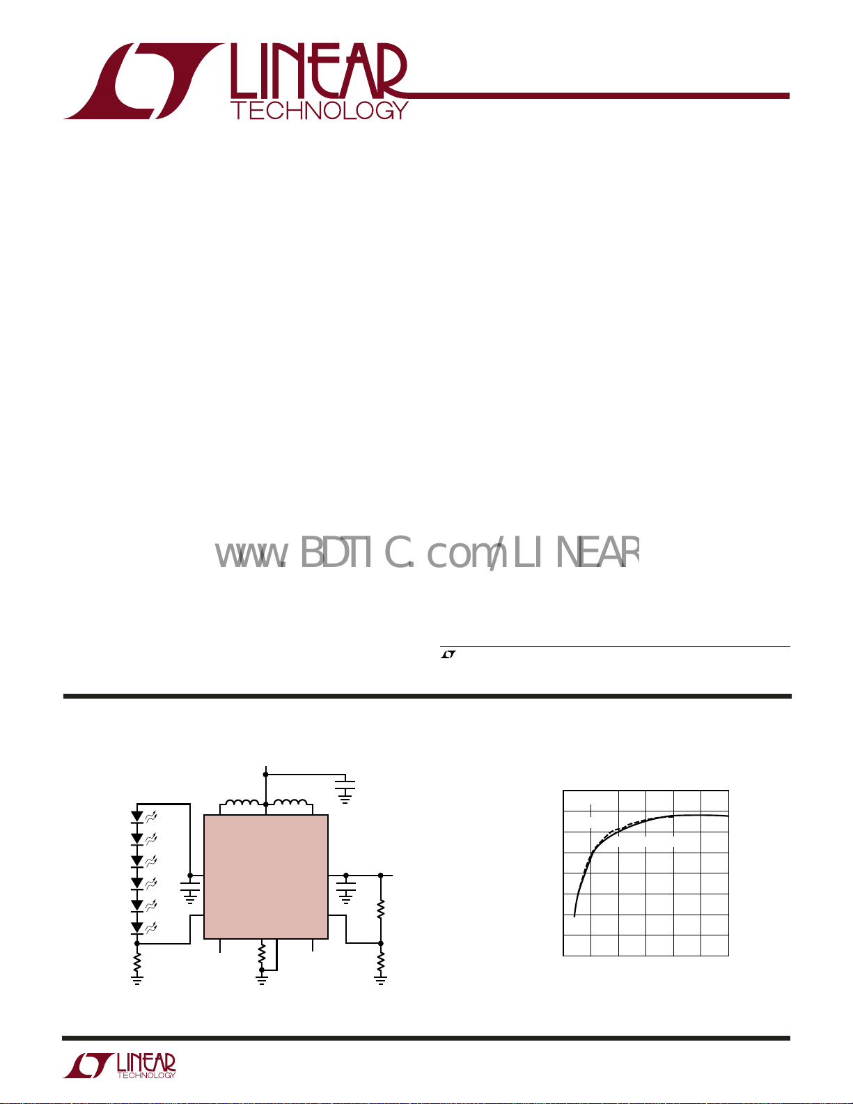
Figure 1. Li-Ion Powered Driver for 6 White LEDs and OLED Display
90
VIN = 3.6V
85
LED DRIVER
80
75
70
65
EFFICIENCY (%)
60
55
50
0
Conversion Efficiency
BOOST CONVERTER
51015
OUTPUT CURRENT (mA)
302520
34661 F01b
34661f
1
LT3466-1
www.BDTIC.com/LINEAR
WWWU
ABSOLUTE AXI U RATI GS
PACKAGE/ORDER I FOR ATIO
UU
W
(Note 1)
Input Voltage (VIN) ................................................... 24V
SW1, SW2 Voltages ................................................ 44V
V
OUT1
, V
Voltages ............................................. 44V
OUT2
CTRL1, CTRL2 Voltages ........................................... 24V
FB1, FB2 Voltages ...................................................... 2V
Operating Temperature Range (Note 2) ... –40°C to 85°C
Storage Temperature Range .................. –65°C to 125°C
Junction Temperature .......................................... 125°C
ELECTRICAL CHARACTERISTICS
range, otherwise specifications are at TA = 25°C. VIN = 3V, V
PARAMETER CONDITIONS MIN TYP MAX UNITS
Minimum Operating Voltage 2.7 V
Maximum Operating Voltage 22 V
FB1 Voltage ● 192 200 208 mV
FB2 Voltage ● 788 800 812 mV
FB1 Pin Bias Current V
FB2 Pin Bias Current V
Quiescent Current V
Switching Frequency RT = 48.7k 0.75 1 1.25 MHz
Oscillator Frequency Range (Note 4) 200 2000 kHz
Nominal RT Pin Voltage RT = 48.7k 0.54 V
Maximum Duty Cycle RT = 48.7k ● 90 96 %
Converter 1 Current Limit ● 310 400 mA
Converter 2 Current Limit ● 310 400 mA
Converter 1 V
Converter 2 V
Switch 1 Leakage Current V
Switch 2 Leakage Current V
CTRL1 Voltage for Full LED Current ● 1.8 V
CTRL2 Voltage for Full Feedback Voltage ● 1V
CTRL1 or CTRL2 Voltage to Turn On the IC 150 mV
CTRL1 and CTRL2 Voltages to Shut Down Chip 70 mV
CTRL1 Pin Bias Current V
CTRL2 Pin Bias Current V
CESAT
CESAT
FB1
FB2
FB1
CTRL1 = CTRL2 = 0V 16 25 µA
R
= 20.5k 92 %
T
RT = 267k 99 %
I
SW1
I
SW2
SW1
SW2
CTRL1
CTRL2
The ● denotes specifications that apply over the full operating temperature
= 3V, V
CTRL1
= 0.2V (Note 3) 10 50 nA
= 0.8V (Note 3) 10 50 nA
= V
= 1V 5 7.5 mA
FB2
= 300mA 320 mV
= 300mA 320 mV
= 10V 0.01 5 µA
= 10V 0.01 5 µA
= 1V ● 6 9 12.5 µA
= 1V (Note 3) ● 10 120 nA
V
OUT1
SW1
V
IN
SW2
V
OUT2
10-LEAD (3mm × 3mm) PLASTIC DFN
T
JMAX
Order Options Tape and Reel: Add #TR
Lead Free: Add #PBF Lead Free Tape and Reel: Add #TRPBF
Lead Free Part Marking: http://www.linear.com/leadfree/
Consult LTC Marketing for parts specified with wider operating temperature ranges.
CTRL2
TOP VIEW
10
9
8
7
6
FB1
CTRL1
R
T
CTRL2
FB2
DD PART MARKING
1
2
11
3
4
5
DD PACKAGE
= 125°C, θJA = 43°C/W, θJC = 3°C/W
EXPOSED PAD (PIN 11) IS GND
MUST BE SOLDERED TO PCB
= 3V, unless otherwise specified.
ORDER PART
NUMBER
LT3466EDD-1
LBRX
34661f
2

LT3466-1
www.BDTIC.com/LINEAR
ELECTRICAL CHARACTERISTICS
range, otherwise specifications are at TA = 25°C. VIN = 3V, V
The ● denotes specifications that apply over the full operating temperature
CTRL1
= 3V, V
= 3V, unless otherwise specified.
CTRL2
PARAMETER CONDITIONS MIN TYP MAX UNITS
V
Overvoltage Threshold 39.5 V
OUT1
V
Overvoltage Threshold 39.5 V
OUT2
Schottky 1 Forward Drop I
Schottky 2 Forward Drop I
Schottky 1 Reverse Leakage V
Schottky 2 Reverse Leakage V
SCHOTTKY1
SCHOTTKY2
OUT1
OUT2
= 300mA 0.85 V
= 300mA 0.85 V
= 20V 5 µA
= 20V 5 µA
Soft-Start Time (Switcher 1) 600 µs
Soft-Start Time (Switcher 2) 600 µs
Note 1: Absolute Maximum Ratings are those values beyond which the life
of a device may be impaired.
Note 3: Current flows out of the pin.
Note 4: Guaranteed by design and test correlation, not production tested.
Note 2: The LTC3466-1E is guaranteed to meet specified performance
from 0°C to 70°C. Specifications over the –40°C to 85°C operating range
are assured by design, characterization and correlation with statistical
process controls.
UW
TYPICAL PERFOR A CE CHARACTERISTICS
TA = 25°C unless otherwise specified
V
OUT1
100mV/DIV
(AC-COUPLED)
V
SW1
20V/DIV
I
100mA/DIV
250
200
150
(mV)
FB1
V
100
Switching Waveforms
(LED Driver)
L1
V
= 3.6V 0.5µs/DIV 34661 G01
IN
6 LEDs AT 20mA
CIRCUIT OF FIGURE 1
V
vs V
50
0
0
FB1
VIN = 3.6V
6 LEDs
0.5
CTRL1
V
CTRL1
1
(V)
1.5
34661 G03
Switching Waveforms
(Boost Converter)
V
OUT2
100mV/DIV
(AC-COUPLED)
V
SW2
20V/DIV
I
L2
100mA/DIV
VIN = 3.6V 0.5µs/DIV 34661 G02
V
= 16V/30mA
OUT2
CIRCUIT OF FIGURE 1
V
vs V
FB2
900
VIN = 3.6V
V
800
700
600
500
(mV)
FB2
400
V
300
200
100
2
0
0
OUT2
= 16V
0.5
CTRL2
V
CTRL2
1
(V)
1.5
34661 G16
2
34661f
3
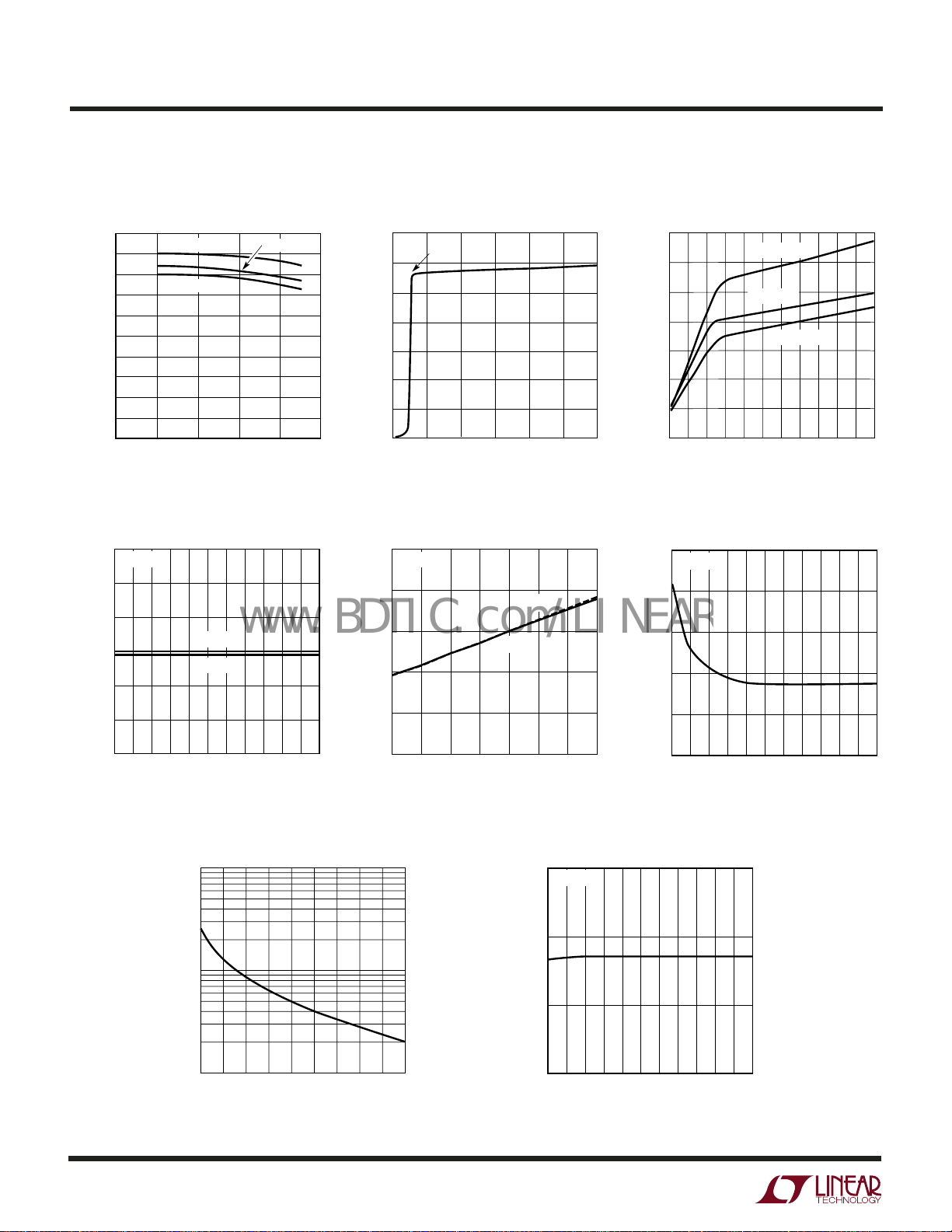
LT3466-1
VIN (V)
2
0
SHUTDOWN CURRENT (µA)
10
30
40
50
70
4
12
16
34661 G06
20
60
10
20
2422
6
8
14 18
TA = –50°C
TA = 25°C
TA = 100°C
www.BDTIC.com/LINEAR
UW
TYPICAL PERFOR A CE CHARACTERISTICS
TA = 25°C unless otherwise specified
500
450
400
350
300
250
200
150
CURRENT LIMIT (mA)
100
50
0
0
TA = –50°C
T
A
20
DUTY CYCLE (%)
= 85°C
40
Open-Circuit Output Clamp
Voltage
41.00
RT = 63.4k
40.50
40.00
39.50
39.00
OUTPUT CLAMP VOLTAGE (V)
38.50
V
V
OUT2
OUT1
60
TA = 25°C
80
34661 G05
100
Quiescent Current
(CTRL1 = CTRL2 = 3V)Switch Current Limit vs Duty Cycle
7
0
UVLO
48
VIN (V)
12 20
6
5
4
3
2
QUIESCENT CURRENT (mA)
1
0
Open-Circuit Output Clamp
Voltage
42
RT = 63.4k
41
40
39
38
OUTPUT CLAMP VOLTAGE (V)
16 24
V
OUT2
V
OUT1
34661 G04
Shutdown Current
(CTRL1 = CTRL2 = 0V)
Input Current with Output 1 and
Output 2 Open Circuit
20
RT = 63.4k
16
12
8
INPUT CURRENT (mA)
4
38.00
6 101418
VIN (V)
2442 8 12 16 20 22
34661 G07
37
–50 –25
0
TEMPERATURE (°C)
RT vs Oscillator Frequency
1000
100
4
(kΩ)
T
R
10
600 180014001000
200
OSCILLATOR FREQUENCY (kHz)
34661 G10
50
25
75
100
Oscillator Frequency vs V
1100
RT = 48.7k
1000
900
OSCILLATOR FREQUENCY (kHz)
800
VIN (V)
0
2
125
34661 G08
8121620
468
IN
34661 G11
10 12
24462 10141822
14 16 20
VIN (V)
18
2422
34661 G09
34661f
UW
www.BDTIC.com/LINEAR
TYPICAL PERFOR A CE CHARACTERISTICS
LT3466-1
TA = 25°C unless otherwise specified
Oscillator Frequency
vs Temperature
1100
VIN = 3.6V
= 48.7k
R
T
1000
900
OSCILLATOR FREQUENCY (kHz)
800
–50
–25 0 25 50
TEMPERATURE (°C)
75
100
34661 G12
CTRL Voltages to Shut Down
the IC
150
= 3.6V
V
IN
125
100
75
50
CTRL VOLTAGE (mV)
25
0
–50
CTRL1
02550
–25
TEMPERATURE (°C)
CTRL2
Schottky Forward Voltage Drop Schottky Leakage Current
400
350
300
250
200
150
100
50
SCHOTTKY FORWARD CURRENT (mA)
0
200 400 800
0
SCHOTTKY FORWARD DROP (mV)
600
1000
34661 G14
8
6
4
2
SCHOTTKY LEAKAGE CURRENT (µA)
0
–50
–25 0 25 50
TEMPERATURE (°C)
75 100
34661 G13
VR = 36V
VR = 20V
75 100
34661 G015
FB2 Pin Voltage vs Temperature
0.810
VIN = 3V
= 16V/30mA
V
OUT2
0.805
0.800
0.795
FB2 VOLTAGE (V)
0.790
0.785
0.780
–50
02550
–25
TEMPERATURE (°C)
75 125100
34661 G17
FB2 Pin Load Regulation
0
–0.20
(%)
–0.40
OUT2
/V
–0.60
OUT2
∆V
–0.80
–1.00
0
10 20
LOAD CURRENT (mA)
V
V
IN
OUT2
= 3V
= 16V
30
34661 G18
34661f
5
LT3466-1
www.BDTIC.com/LINEAR
U
UU
PI FU CTIO S
V
(Pin 1): Output of Converter 1. This pin is connected
OUT1
to the cathode of the internal Schottky diode. Connect an
output capacitor from this pin to ground.
SW1 (Pin 2): Switch Pin for Converter 1. Connect the
inductor at this pin.
VIN (Pin 3): Input Supply Pin. Must be locally bypassed
with a 1µF, X5R or X7R type ceramic capacitor.
SW2 (Pin 4): Switch Pin for Converter 2. Connect the
inductor at this pin.
V
(Pin 5): Output of Converter 2. This pin is connected
OUT2
to the cathode of the internal Schottky diode. Connect an
output capacitor from this pin to ground.
FB2 (Pin 6): Feedback Pin for Converter 2. The nominal
voltage at this pin is 800mV. Connect the resistor divider
to this pin. The feedback voltage can be programmed
as:
V
≈ V
FB2
V
= 0.8V, when V
FB2
CTRL2
, when V
CTRL2
CTRL2
> 1V
< 0.8V
CTRL2 (Pin 7): Dimming and Shutdown Pin for Converter 2. As the pin voltage is ramped from 0V to 1V, the
FB2 pin voltage tracks the CTRL2 voltage and ramps up to
0.8V. Any voltage above 1V does not affect the feedback
voltage. Do not leave the pin floating. It must be connected
to ground to disable converter 2.
RT (Pin 8): Timing Resistor to Program the Switching
Frequency. The switching frequency can be programmed
from 200KHz to 2MHz.
CTRL1 (Pin 9): Dimming and Shutdown Pin for Converter 1. Connect this pin to ground to disable the converter. As the pin voltage is ramped from 0V to 1.8V, the
LED current ramps from 0 to I
voltage above 1.8V does not affect the LED current.
FB1 (Pin 10): Feedback Pin for Converter 1. The nominal
voltage at this pin is 200mV. Connect cathode of the lowest
LED and the feedback resistor at this pin. The LED current
can be programmed by :
I
≈ (V
LED1
I
≈ (200mV/R
LED1
CTRL1
/5 • R
FB1
), when V
FB1
), when V
(= 200mV/R
LED1
CTRL1
CTRL1
< 1V
> 1.8V
FB1
). Any
Exposed Pad (Pin 11): The Exposed Pad must be soldered
to the PCB system ground.
6
34661f

BLOCK DIAGRA
–
+
–
+
Σ
–
+
+
EAEA
PWM
COMP
R
SNS1
R
SNS2
OSC
C3
V
OUT2
DRIVER
L2
SW2
0.8V
EXPOSED
PAD
20k
FB1
CONVERTER 1 CONVERTER 2
0.2V
80k
SHDN
CTRL2
7
11
CTRL1
9
–
+
–
+
+
START-UP
CONTROL
REF 1.25V
PWM
LOGIC
5
4
V
IN
V
IN
R
T
3
R
T
8
FB2
R2
R1
R
FB1
34661 F02
6
–
+
Σ
OSC
SW1
C1
L1
DRIVER
1
2
10
V
OUT1
C2
PWM
LOGIC
OSC
RAMP
GEN
OSC
OVERVOLT
DETECTION
OVERVOLT
DETECTION
Q1 Q2
A2
A1 A1
A2
A3
PWM
COMP
A3
www.BDTIC.com/LINEAR
LT3466-1
W
Figure 2. Block Diagram
34661f
7

LT3466-1
www.BDTIC.com/LINEAR
OPERATIO
U
Main Control Loop
The LT3466-1 uses a constant frequency, current mode
control scheme to provide excellent line and load regulation. It incorporates two similar, but fully independent PWM
converters. Operation can be best understood by referring
to the Block Diagram in Figure 2. The oscillator, start-up
bias and the bandgap reference are shared between the
two converters. The control circuitry, power switch, Schottky diode etc., are similar for both converters.
At power-up, the output voltages V
charged up to V
(input supply voltage) via their respec-
IN
OUT1
and V
OUT2
are
tive inductor and the internal Schottky diode. If either
CTRL1 and CTRL2 or both are pulled high, the bandgap
reference, start-up bias and the oscillator are turned on.
Working of the main control loop can be understood by
following the operation of converter 1. At the start of each
oscillator cycle, the power switch Q1 is turned on. A
voltage proportional to the switch current is added to a
stabilizing ramp and the resulting sum is fed into the
positive terminal of the PWM comparator A2. When this
voltage exceeds the level at the negative input of A2, the
PWM logic turns off the power switch. The level at the
negative input of A2 is set by the error amplifier A1, and is
simply an amplified version of the difference between the
feedback voltage and the 200mV reference voltage. In this
manner, the error amplifier A1 regulates the voltage at the
FB1 pin to 200mV. The output of the error amplifier A1 sets
the correct peak current level in inductor L1 to keep the
output in regulation. The CTRL1 pin voltage is used to
adjust the feedback voltage.
The working of converter 2 is similar to converter 1 with
the exception that the feedback 2 reference voltage is
800mV. The error amplifier A1 in converter 2 regulates the
voltage at the FB2 pin to 800mV. If only one of the
converters is turned on, the other converter will stay off
and its output will remain charged up to VIN (input supply
voltage). The LT3466-1 enters into shutdown, when both
CTRL1 and CTRL2 are pulled lower than 70mV. The CTRL1
and CTRL2 pins perform independent dimming and shutdown control for the two converters.
Minimum Output Current
The LT3466-1 can drive a 6-LED string at 3mA LED current
without pulse skipping. As current is further reduced, the
device may begin skipping pulses. This will result in some
low frequency ripple, although the LED current remains
regulated on an average basis down to zero. The photo in
Figure 3 shows circuit operation with 6 white LEDs at 3mA
current driven from 3.6V supply. Peak inductor current is
less than 50mA and the regulator operates in discontinuous mode implying that the inductor current reached zero
during the discharge phase. After the inductor current
reaches zero, the switch pin exhibits ringing due to the LC
tank circuit formed by the inductor in combination with
switch and diode capacitance. This ringing is not harmful;
far less spectral energy is contained in the ringing than in
the switch transitions. The ringing can be damped by
application of a 300Ω resistor across the inductors, although this will degrade efficiency.
V
OUT1
20mV/DIV
(AC-COUPLED)
V
SW1
20V/DIV
I
L1
50mA/DIV
V
= 3.6V 0.5µs/DIV 34661 F03
IN
I
= 3mA
LED1
CIRCUIT OF FIGURE 1
Figure 3. Switching Waveforms
Overvoltage Protection
The LT3466-1 has internal overvoltage protection for both
converters. In the event the white LEDs are disconnected
from the circuit or fail open, the converter 1 output voltage
is clamped at 39.5V (typ). Figure 4(a) shows the transient
response of the circuit in Figure 1 with LED1 disconnected.
With the white LEDs disconnected, the converter 1 starts
switching at the peak current limit. The output of converter
1 starts ramping up and finally gets clamped at 39.5V (typ).
The converter 1 will then switch at low inductor current to
regulate the output voltage. Output voltage and input
current during output open circuit are shown in the Typical
Performance Characteristics graphs.
8
34661f

OPERATIO
www.BDTIC.com/LINEAR
LT3466-1
U
In the event one of the converters has an output open-circuit,
its output voltage will be clamped at 39.5V. However, the
other converter will continue functioning properly. The photo
in Figure 4b shows circuit operation with converter 1 output
open-circuit and converter 2 driving the OLED display. Converter 1 starts switching at a lower inductor current and
begins skipping pulses, thereby reducing its input current.
Converter 2 continues functioning properly.
V
OUT1
10V/DIV
I
L1
200mA/DIV
200µs/DIV
LED1 DISCONNECTED AT THIS POINT
V
= 3.3V
IN
CIRCUIT OF FIGURE 1
Figure 4a. Transient Response of Switcher 1 with LED1
Disconnected from the Output
34661 F04a
Soft-Start
The LT3466-1 has a separate internal soft-start circuitry
for each converter. Soft-start helps to limit the inrush
current during start-up. Soft-start is achieved by clamping
the output of the error amplifier during the soft-start
period. This limits the peak inductor current and ramps up
the output voltage in a controlled manner.
The converter enters into soft-start mode whenever the
respective CTRL pin is pulled from low to high. Figure 5
shows the start-up waveforms with converter 1 driving six
LEDs at 20mA. The filtered input current, as shown in
Figure 5, is well controlled. The soft-start circuitry is less
effective when driving a higher number of LEDs.
Undervoltage Lockout
The LT3466-1 has an undervoltage lockout circuit which
shuts down both converters when the input voltage drops
below 2.1V (typ). This prevents the converter from switching in an erratic mode when powered from low supply
voltages.
V
SW1
50V/DIV
100mA/DIV
V
SW2
50V/DIV
100mA/DIV
I
IN
200mA/DIV
I
L1
I
L2
V
= 3.6V
IN
CIRCUIT OF FIGURE 1
1µs/DIV
34661 F04b
V
OUT1
20V/DIV
V
FB1
200mV/DIV
CTRL1
5V/DIV
V
= 3.6V
IN
6 LEDs, 20mA
CIRCUIT OF FIGURE 1
200µs/DIV
Figure 4b. Output 1 Open-Circuit Waveforms Figure 5. Start-Up Waveforms
34661 F05
34661f
9

LT3466-1
www.BDTIC.com/LINEAR
WUUU
APPLICATIO S I FOR ATIO
DUTY CYCLE
The duty cycle for a step-up converter is given by:
VVV
++–
D
OUT D IN
=
VVV
OUT D CESAT
–
where:
= Output voltage
V
OUT
V
= Schottky forward voltage drop
D
V
= Saturation voltage of the switch
CESAT
= Input battery voltage
V
IN
The maximum duty cycle achievable for LT3466
-1
is 96%
(typ) when running at 1MHz switching frequency. It increases to 99% (typ) when run at 200kHz and drops to
92% (typ) at 2MHz. Always ensure that the converter is not
duty-cycle limited when powering the LEDs or OLED at a
given switching frequency.
SETTING THE SWITCHING FREQUENCY
OPERATING FREQUENCY SELECTION
The choice of operating frequency is determined by several factors. There is a tradeoff between efficiency and
component size. Higher switching frequency allows the
use of smaller inductors albeit at the cost of increased
switching losses and decreased efficiency.
Another consideration is the maximum duty cycle achievable. In certain applications, the converter needs to operate at the maximum duty cycle in order to light up the
-1
maximum number of LEDs. The LT3466
has a fixed
oscillator off-time and a variable on-time. As a result, the
maximum duty cycle increases as the switching frequency
is decreased.
The circuit of Figure 1 is operated with different values of
timing resistor (RT). RT is chosen so as to run the
converters at 800kHz (RT = 63.4k), 1.25MHz (RT = 38.3k)
and 2MHz (RT = 20.5k). The efficiency comparison for
different RT values is shown in Figure 7.
INDUCTOR SELECTION
The LT3466-1 uses a constant frequency architecture that
can be programmed over a 200KHz to 2MHz range with a
single external timing resistor from the R
The nominal voltage on the R
pin is 0.54V, and the
T
pin to ground.
T
current that flows into the timing resistor is used to
charge and discharge an internal oscillator capacitor. A
graph for selecting the value of R
for a given operating
T
frequency is shown in the Figure 6.
1000
100
(kΩ)
T
R
10
600 180014001000
200
OSCILLATOR FREQUENCY (kHz)
34661 F06
The choice of the inductor will depend on the selection of
switching frequency of LT3466-1. The switching frequency can be programmed from 200kHz to 2MHz. Higher
switching frequency allows the use of smaller inductors
albeit at the cost of increased switching losses.
90
CIRCUIT OF FIGURE 1
= 3.6V
V
IN
6 LEDs
80
70
60
EFFICIENCY (%)
50
40
0
5
LED CURRENT (mA)
RT = 63.4k
RT = 38.3k
10
RT = 20.5k
15
20
34661 F07
Figure 6. Timing Resistor (RT) Value
10
Figure 7. Efficiency Comparison for Different RT Resistors
34661f

WUUU
www.BDTIC.com/LINEAR
APPLICATIO S I FOR ATIO
LT3466-1
The inductor current ripple (∆IL), neglecting the drop
across the Schottky diode and the switch, is given by :
VV V
∆ =
IN MIN OUT MAX IN MIN
I
L
•–
() ( ) ()
()
VfL
OUT MAX
••
()
where:
L = Inductor
f = Operating frequency
V
V
= Minimum input voltage
IN(MIN)
OUT(MAX)
= Maximum output voltage
The ∆IL is typically set to 20% to 40% of the maximum
inductor current.
The inductor should have a saturation current rating
greater than the peak inductor current required for the
application. Also, ensure that the inductor has a low DCR
(copper wire resistance) to minimize I2R power losses.
Recommended inductor values range from 10µH to 68µH.
Several inductors that work well with the LT3466-1 are listed
in Table 1. Consult each manufacturer for more detailed
information and for their entire selection of related parts.
Table 1. Recommended Inductors
MAX CURRENT
L DCR RATING
PART (µH) (Ω) (mA) VENDOR
LQH32CN100 10 0.44 300 Murata
LQH32CN150 15 0.58 300 (814) 237-1431
LQH43CN330 33 1.00 310 www.murata.com
ELL6RH330M 33 0.38 600 Panasonic
ELL6SH680M 68 0.52 500 (714) 373-7939
www.panasonic.com
A914BYW330M 33 0.45 440 Toko
A914BYW470M 47 0.73 360 www.toko.com
A920CY680M 68 0.40 400
CDRH2D18150NC 15 0.22 0.35A Sumida
CDRH4D18-330 33 0.51 0.31A (847) 956-0666
CDRH5D18-680 68 0.84 0.43A www.sumida.com
CAPACITOR SELECTION
The small size of ceramic capacitors make them ideal for
LT3466-1 applications. Use only X5R and X7R types
because they retain their capacitance over wider voltage
and temperature ranges than other types such as Y5V or
Z5U. A 1µF input capacitor is sufficient for most applica-
tions. Always use a capacitor with sufficient voltage rating.
Table 2 shows a list of several ceramic capacitor manufacturers. Consult the manufacturers for detailed information
on their entire selection of ceramic parts.
Table 2. Ceramic Capacitor Manufacturers
Taiyo Yuden (408) 573-4150
www.t-yuden.com
AVX (803) 448-9411
www.avxcorp.com
Murata (714) 852-2001
www.murata.com
INRUSH CURRENT
The LT3466-1 has built-in Schottky diodes. When supply
voltage is applied to the VIN pin, an inrush current flows
through the inductor and the Schottky diode and charges
up the output capacitor. Both Schottky diodes in the
LT3466-1 can sustain a maximum of 1A current. The
selection of inductor and capacitor value should ensure
the peak of the inrush current to be below 1A.
For low DCR inductors, which is usually the case for this
application, the peak inrush current can be simplified as
follows:
V
–.:06
PK
IN
=
ω
L
I
where
1
=
ω
LC
OUT
Table 3 gives inrush peak current for some component
selections.
Table 3. Inrush Peak Current
VIN (V) L (µH) C
5 15 0.47 0.78
5 33 1.00 0.77
5 47 2.2 0.95
5 68 1.00 0.53
9 47 0.47 0.84
12 33 0.22 0.93
(µF) IP (A)
OUT
34661f
11

LT3466-1
VV
R
R
OUT2
08 1
1
2
=+
⎛
⎝
⎜
⎞
⎠
⎟
.
www.BDTIC.com/LINEAR
WUUU
APPLICATIO S I FOR ATIO
Typically peak inrush current will be less than the value
calculated above. This is due to the fact that the DC
resistance in the inductor provides some damping resulting in a lower peak inrush current.
SETTING THE LED CURRENT
The current in the LED string can be set by the choice of the
resistor R
(Figure 1). The feedback reference is 200mV.
FB1
In order to have accurate LED current, precision resistors
are preferred (1% is recommended).
FB
200
=
I
LED11
Value Selection
FB1
I
(mA) R
LED1
5 40.2
10 20.0
15 13.3
20 10.0
25 8.06
FB1
(Ω)
R
Table 4. R
mV
Most White LEDs are driven at maximum currents of
15mA to 20mA.
Feedback voltage variation versus control voltage is given
in the Typical Performance Characteristics graphs.
Using a Filtered PWM Signal
A variable duty cycle PWM can be used to control the
brightness of the LED string. The PWM signal is filtered
(Figure 8) by an RC network and fed to the CTRL1 pin.
The corner frequency of R1, C1 should be much lower than
the frequency of the PWM signal. R1 needs to be much
smaller than the internal impedance in the CTRL pin, which
is 100kΩ.
C1
1µF
LT3466-1
CTRL1
34661 F08
R1
10k
PWM
10kHz TYP
Figure 8. Dimming Control Using a Filtered PWM Signal
SETTING THE BOOST OUTPUT VOLTAGE
The LT3466-1 regulates the voltage at the FB2 pin to 0.8V.
The output voltage of the boost converter (V
OUT2
) is set by
a resistor divider according to the formula:
DIMMING WHITE LEDS
The LED current in the driver can be set by modulating the
CTRL1 pin. There are two different ways to control the
intensity of white LEDs.
Using a DC Voltage
For some applications, the preferred method of brightness
control is a variable DC voltage to adjust the LED current.
The CTRL1 pin voltage can be modulated to set the
dimming of the LED string. As the voltage on the CTRL1
pin increases from 0V to 1.8V, the LED current increases
from 0 to I
. As the CTRL1 pin voltage increases
LED1
beyond 1.8V, it has no effect on the LED current.
The LED current can be set by:
I
≈ (V
LED1
I
≈ (200mV/R
LED1
CTRL1
/5 • R
FB1
), when V
FB1
), when V
CTRL1
CTRL1
< 1V
> 1.8V
Choose 1% resistors for better accuracy. The FB2 input
bias current is quite low, on the order of 10nA (typ). Large
resistor values (R1 ~ 1MΩ) can be used in the divider
network maximizing efficiency.
PROGRAMMING THE BOOST OUTPUT VOLTAGE
The output voltage of the boost converter can be modulated by applying a variable DC voltage at the CTRL2 pin
The nominal voltage at the FB2 pin is 800mV. As the
voltage on the CTRL2 pin is ramped from 0V to 1V, the FB2
pin voltage ramps up to 0.8V. The feedback voltage can be
programmed as:
V
≈ V
FB2
V
≈ 0.8V, when V
FB2
CTRL2
, when V
CTRL2
CTRL2
> 1V
< 0.8V
34661f
12

WUUU
VIRVVV
IN MAX BASE BASE BE Q OUT CE Q( ) () ()
+• + = +
121
www.BDTIC.com/LINEAR
APPLICATIO S I FOR ATIO
LT3466-1
Figure 9 shows the feedback voltage variation versus the
control voltage. As seen in Figure 9, the linearity of the
graph allows the feedback voltage to be set accurately via
the control voltage.
The boost converter output voltage (V
R
1
VV
=+
OUT FB22
⎛
⎜
⎝
⎞
1
⎟
⎠
R
2
) is given by:
OUT2
Thus a linear change in the feedback (FB2) voltage results
in a linear change in the boost output voltage (V
OUT2
).
Connect the CTRL2 pin to ground to disable converter 2.
Do not leave the pin floating. Unlike the CTRL1 pin, which
has an internal 100k pull-down resistor, the CTRL2 pin
input impedance is very high (>100MΩ). A small amount
of board leakage current is sufficient to turn on the
converter 2.
900
VIN = 3.6V
= 16V
V
OUT2
800
700
600
500
(mV)
FB2
400
V
300
200
100
0
0
0.8
0.4
V
CTRL2
Figure 9. V
FB2
(V)
vs V
1.61.2
CTRL2
2
34661 F09
OUTPUT DISCONNECT
The LT3466-1 can be used for powering white LEDs
(Channel 1) and an OLED display or, LCD bias (Channel 2).
Some OLED displays require load isolation in order to
reduce the current drained from the battery in shutdown.
The LT3466-1 output can be configured to provide output
disconnect by the use of only one resistor, R
BASE
, and a
PNP transistor, Q1, as shown in Figure 10.
As a design example, we target a Li-Ion powered driver for
6 white LEDs and an OLED display (16V at 30mA). We can
choose a general purpose PNP switching transistor like
Philips BC807 (Q1) to provide isolation.
3V TO 5V
C
IN
I
R
C
OUT1
1µF
R
FB1
10Ω
: TAIYO YUDEN JMK107BJ105
C
IN
: TAIYO YUDEN GMK316BJ105
C
OUT1
, C
C
OUT2
L1, L2: TOKO D52LC
Q1: PHILIPS BC807
: TAIYO YUDEN TMK316BJ474
OUT3
L1
33µH
SW1 SW2V
IN
V
OUT1
LT3466-1
FB1
R
CTRL1 CTRL2
T
1µF
63.4k
1%
V
BASE
L2
33µH
OUT2
FB2
ONOFFONOFF
BASE
Q1
+–
V
CE(SAT)
R1
475k
C
OUT2
0.47µF
Figure 10. Li-Ion Powered Driver for 6 White LEDs and a
Secondary OLED Display with Output Disconnect
The R
I
LOAD
I
BASE
I
BASE
all conditions. The h
resistor can be calculated as:
BASE
= 30mA
I
LOAD
=
h
04.
FE MIN
()
must be chosen such that Q1 is in saturation under
can be obtained from the
FE(MIN)
Philips BC807 data sheet as:
h
This yields worst case I
I
BASE
R
BASE
≅ 100
FE(MIN)
= ≅
0 4 100
is given by:
mA
30
.( )
BASE
075
.
as:
mA
Thus R
;
BASE
VV V V
=
––
211
OUT IN MAX CE Q BE Q
+
( ) () ()
I
B
AASE
R2
24.9k
34661 F10
16V
30mA
C
OUT3
0.47µF
34661f
13

LT3466-1
www.BDTIC.com/LINEAR
WUUU
APPLICATIO S I FOR ATIO
The V
CE(SAT)
and V
BE(SAT)
values for the transistor Q1 can
be obtained from the Philips BC807 data sheet:
R
R
BASE
BASE
VV
=
= 13.6k
+1650109
–.–.
mA
075
.
Picking the closest 1% resistor value yields:
R
= 14k
BASE
BOARD LAYOUT CONSIDERATION
As with all switching regulators, careful attention must be
paid to the PCB board layout and component placement.
To prevent electromagnetic interference (EMI) problems,
proper layout of high frequency switching paths is essential. Minimize the length and area of all traces connected to
the switching node pins (SW1 and SW2). Keep the feedback pins (FB1 and FB2) away from the switching nodes.
The DFN package has an exposed paddle that must be
connected to the system ground. The ground connection
for the feedback resistors should be tied directly to the
ground plane and not shared with any other component,
except the R
resistor, ensuring a clean, noise-free con-
T
nection. Recommended component placement is shown
in the Figure 11.
GND
C
IN
V
GND
C
OUT1
R
FB1
L1
IN
L2
C
OUT2
Figure 11. Recommended Component Placement
1
2
11
3
4
5
10
9
8
7
6
R2
R1
CTRL1
R
T
CTRL2
34661 F10
14
34661f

U
www.BDTIC.com/LINEAR
TYPICAL APPLICATIO S
Li-Ion Powered 4 White LEDs Driver and 12V Boost Converter
3V TO 5V
C
IN
1µF
12V
30mA AT V
60mA AT V
R1
R2
64.9k
34661 TA01a
4 LEDs
C
OUT1
0.47µF
R
FB1
10Ω
C
: TAIYO YUDEN JMK107BJ105
IN
: TAIYO YUDEN EMK212BJ474
C
OUT1
: TAIYO YUDEN EMK212BJ105
C
OUT2
L1, L2: MURATA LQH32CN150K53
L1
15µH
SW1 SW2V
IN
V
OUT1
LT3466-1
FB1
R
CTRL1 CTRL2
T
38.3k
1%
V
OUT2
FB2
L2
15µH
909k
C
OUT2
1µF
ONOFFONOFF
IN
IN
= 3V
= 5V
Efficiency vs Load Current
90
4 LEDs/20mA
V
OUT2
85
80
75
EFFICIENCY (%)
70
65
60
0
10
= 12V
VIN = 3V
20 30 40
LOAD CURRENT (mA)
LT3466-1
VIN = 5V
50 60
34661 TA01b
Li-Ion Powered Driver for 6 White LEDs and OLED Display
3V TO 5V
6 LEDs
R
FB1
10Ω
: TAIYO YUDEN JMK107BJ105
C
IN
C
OUT1
L1, L2: 33µH TOKO D52LC
SW1 SW2V
V
C
OUT1
1µF
, C
OUT2
OUT1
FB1
CTRL1 GND CTRL2
SHUTDOWN
AND DIMMING
CONTROL 1
: TAIYO YUDEN GMK316BJ105
L1
33µH
63.4k
IN
LT3466-1
R
T
L2
33µH
V
SHUTDOWN
AND DIMMING
CONTROL 2
OUT2
FB2
1µF
C
1µF
OUT2
16V
30mA
R1
475k
R2
24.9k
34661 TA02a
90
85
LED DRIVER
80
75
70
65
EFFICIENCY (%)
60
VIN = 3.6V
55
6 LEDs
V
OUT2
50
0
Conversion Efficiency
BOOST CONVERTER
= 16V
51015
OUTPUT CURRENT (mA)
302520
34661 TA02b
34661f
15

LT3466-1
www.BDTIC.com/LINEAR
TYPICAL APPLICATIO S
Li-Ion Powered Driver for 6 White LEDs and OLED with Output Disconnect
U
V
OUT2
20V/DIV
6 LEDs
L1
33µH
C
OUT1
1µF
R
FB1
10Ω
: TAIYO YUDEN JMK107BJ105
C
IN
: TAIYO YUDEN GMK316BJ105
C
OUT1
, C
C
OUT2
OUT3
L1, L2: 33µH TOKO D52LC
Q1: PHILIPS BC807
V
FB1
CTRL1 CTRL2
: TAIYO YUDEN TMK316BJ474
3V TO 5V
SW1 SW2V
OUT1
LT3466-1
14k
C
IN
1µF
L2
33µH
IN
V
OUT2
FB2
R
T
63.4k
1%
ONOFFONOFF
C
OUT3
0.47µF
C
OUT2
0.47µF
Q1
16V
30mA
R1
475k
R2
24.9k
34661 TA03a
Conversion Efficiency
90
VIN = 3.6V
= 16V
V
OUT2
80
200mA/DIV
CTRL2
5V/DIV
I
L2
34661 TA03c
V
= 3.6V
IN
OUT2
= 16V
2ms/DIVV
70
60
EFFICIENCY (%)
50
40
0
10 15 20
5
LOAD CURRENT (mA)
25 30
34661 TA03b
34661f
16

TYPICAL APPLICATIO S
www.BDTIC.com/LINEAR
Li-Ion Powered Driver for 6 White LEDs and OLED with Output Disconnect
6 LEDs
U
R
FB1
10Ω
C
OUT1
1µF
3V TO 5V
L1
33µH
SW1 SW2V
V
OUT1
LT3466-1
FB1
R
CTRL1 CTRL2
IN
T
63.4k
1%
C
1µF
V
IN
OUT2
FB2
L2
33µH
LT3466-1
16V
Q1
C
OUT3
0.47µF
C
OUT2
0.47µF
ONOFFONOFF
30mA
R1
475k
R2
24.9k
34661 TA04a
V
OUT2
20V/DIV
I
200mA/DIV
CTRL2
5V/DIV
: TAIYO YUDEN JMK107BJ105
C
IN
: TAIYO YUDEN GMK316BJ105
C
OUT1
, C
C
OUT2
L1, L2: 33µH TOKO D52LC
Q1: SILICONIX TPO610
: TAIYO YUDEN TMK316BJ474
OUT3
NOTE: ENSURE THAT V
OUT2
> V
IN(MAX)
+ 5V
Conversion Efficiency
90
VIN = 3.6V
= 16V
V
OUT2
85
80
L2
34661 TA04c
V
= 3.6V
IN
OUT2
= 16V
2ms/DIVV
75
70
65
EFFICIENCY (%)
60
55
50
0
510 20
15
LOAD CURRENT (mA)
25
34661 TA04b
30
34661f
17

LT3466-1
www.BDTIC.com/LINEAR
U
TYPICAL APPLICATIO S
Li-Ion to 10 White LEDs and LCD Bias (±8V) with Output Disconnect
10 LEDs
R
FB1
16.5Ω
: TAIYO YUDEN JMK107BJ105
C
IN
: TAIYO YUDEN UMK325BJ105
C
OUT1
, C
C
OUT2
C1, C2: TAIYO YUDEN UMK212BJ104
D1, D2: PHILIPS BAT54S
L1: 68µH TOKO D52LC
L2: 33µF TOKO D52LC
L1
68µH
SW1 SW2V
V
C
OUT1
1µF
: TAIYO YUDEN GMK316BJ105
OUT3
OUT1
FB1
CTRL1 CTRL2
ONOFF
3V TO 5V
IN
LT3466-1
R
T
147k
1µF
V
C
OUT2
IN
FB2
L2
33µH
ONOFF
C1
0.1µF
C2
0.1µF
D1
–8V
10mA
C
OUT2
1µF
D2
909k
10k
34661 TA05a
C
1µF
8V
10mA
OUT3
+8V OUTPUT
10V/DIV
–8V OUTPUT
10V/DIV
CTRL2
5V/DIV
= 3.6V
IN
+8V/10mA
–8V/10mA
Conversion Efficiency
84
VIN = 3.6V
10 LEDs
82
+8V/10mA
–8V/10mA
80
78
EFFICIENCY (%)
76
2ms/DIVV
34661 TA05c
74
72
0
468
2
LED CURRENT (mA)
10 12
34661 TA05b
18
34661f

PACKAGE DESCRIPTIO
www.BDTIC.com/LINEAR
LT3466-1
U
DD Package
10-Lead Plastic DFN (3mm × 3mm)
(Reference LTC DWG # 05-08-1699)
0.675 ±0.05
3.50 ±0.05
1.65 ±0.05
(2 SIDES)2.15 ±0.05
PACKAGE
OUTLINE
0.25 ± 0.05
2.38 ±0.05
RECOMMENDED SOLDER PAD PITCH AND DIMENSIONS
PIN 1
TOP MARK
(SEE NOTE 6)
0.200 REF
NOTE:
1. DRAWING TO BE MADE A JEDEC PACKAGE OUTLINE M0-229 VARIATION OF (WEED-2).
CHECK THE LTC WEBSITE DATA SHEET FOR CURRENT STATUS OF VARIATION ASSIGNMENT
2. DRAWING NOT TO SCALE
3. ALL DIMENSIONS ARE IN MILLIMETERS
4. DIMENSIONS OF EXPOSED PAD ON BOTTOM OF PACKAGE DO NOT INCLUDE
MOLD FLASH. MOLD FLASH, IF PRESENT, SHALL NOT EXCEED 0.15mm ON ANY SIDE
5. EXPOSED PAD SHALL BE SOLDER PLATED
6. SHADED AREA IS ONLY A REFERENCE FOR PIN 1 LOCATION ON THE
TOP AND BOTTOM OF PACKAGE
0.50
BSC
(2 SIDES)
3.00 ±0.10
(4 SIDES)
0.75 ±0.05
1.65 ± 0.10
(2 SIDES)
0.00 – 0.05
R = 0.115
TYP
2.38 ±0.10
(2 SIDES)
BOTTOM VIEW—EXPOSED PAD
106
15
0.25 ± 0.05
0.50 BSC
0.38 ± 0.10
(DD10) DFN 1103
Information furnished by Linear Technology Corporation is believed to be accurate and reliable.
However, no responsibility is assumed for its use. Linear Technology Corporation makes no representation that the interconnection of its circuits as described herein will not infringe on existing patent rights.
34661f
19

LT3466-1
www.BDTIC.com/LINEAR
TYPICAL APPLICATIO
Li-Ion to 8 White LEDs and ±15V TFT LCD Bias Supply
3V TO 5V
L1
33µH
SW1 SW2V
8 LEDs
C
OUT1
1µF
V
OUT1
FB1
CTRL1 CTRL2
IN
LT3466-1
R
T
1µF
V
U
C
IN
OUT2
FB2
L2
33µH
C1
0.1µF
475k
26.7k
Conversion Efficiency
D1
–15V
10mA
C
OUT3
1µF
15V
10mA
C
OUT2
1µF
86
VIN = 3.6V
8 LEDs
84
+15V/10mA
–15V/10mA
82
80
EFFICIENCY (%)
78
76
R
FB1
13.3Ω
CIN: TAIYO YUDEN JMK107BJ105
, C
C
OUT1
OUT2
C1: TAIYO YUDEN UMK212BJ104
L1, L2: 33µH TOKO D52LC
D1: PHILIPS BAT54S
ONOFF
, C
: TAIYO YUDEN GMK316BJ105
OUT3
63.4k
ONOFF
RELATED PARTS
PART NUMBER DESCRIPTION COMMENTS
LT1618 Constant Current, Constant Voltage 1.4MHz, High Efficiency VIN: 1.6V to 18V, V
Boost Regulator MS/EDD Packages
LT1932 Constant Current, 1.2MHz, High Efficiency White LED Boost VIN: 1V to 10V, V
Regulator ThinSOT
LT1937 Constant Current, 1.2MHz, High Efficiency White LED Boost VIN: 2.5V to 10V, V
Regulator ThinSOT, SC70 Packages
LTC®3200-5 Low Noise, 2MHz, Regulated Charge Pump White LED Driver VIN: 2.7V to 4.5V, V
LTC3202 Low Noise, 1.5MHz, Regulated Charge Pump White LED Driver VIN: 2.7V to 4.5V, V
LTC3205 High Efficiency, Multidisplay LED Controller VIN: 2.8V to 4.5V, V
LTC3216 1A Low Noise High Current LED Charge Pump with Independent VIN: 2.9V to 4.4V, V
Flash/Torch Current Control DFN Package
LTC3453 500mA Synchronous Buck-Boost High Current LED Driver VIN: 2.7V to 5.5V, V
in Q FN QFN Package
LT3465/LT3465A Constant Current, 1.2MHz/2.7MHz, High Efficiency White LED VIN: 2.7V to 16V, V
Boost Regulator with Integrated Schottky Diode ThinSOT Package
LT3466 Dual Constant Current, 2MHz High Efficiency White LED Boost VIN: 2.7V to 24V, V
Regulator with Integrated Schottky Diode DFN Package
LT3479 3A, Full Featured DC/DC Converter with Soft-Start and Inrush VIN: 2.5V to 24V, V
Current Protection DFN/TSSOP Packages
ThinSOT is a trademark of Linear Technology Corporation.
Linear Technology Corporation
20
1630 McCarthy Blvd., Milpitas, CA 95035-7417
(408) 432-1900 ● FAX: (408) 434-0507
●
www.linear.com
34661 TA06a
74
TM
Package
ThinSOT Package
MS/EDD Packages
QFN-24 Package
0
2.5
OUT(MAX)
OUT(MAX)
OUT(MAX)
OUT(MAX)
OUT(MAX)
OUT(MAX)
OUT(MAX)
OUT(MAX)
OUT(MAX)
OUT(MAX)
OUT(MAX)
5 7.5 10
LED CURRENT (mA)
12.5 15
34661 TA06b
= 34V, IQ = 1.8mA, ISD < 1µA,
= 34V, IQ = 1.2mA, ISD < 1µA,
= 34V, IQ = 1.9mA, ISD < 1µA,
= 5V, IQ = 8mA, ISD < 1µA,
= 5.5V, IQ = 5mA, ISD < 1µA,
= 6V, IQ = 50µA, ISD < 1µA,
= 5.5V, IQ = 300µA, ISD < 2.5µA,
= 5.5V, IQ = 0.6mA, ISD < 6µA,
= 34V, IQ = 1.9mA, ISD < 1µA,
= 40V, IQ = 5mA, ISD < 16µA,
= 40V, IQ = 6.5mA, ISD < 1µA,
34661f
LT/TP 0705 500 • PRINTED IN USA
© LINEAR TECHNOLOGY CORPORATION 2005
 Loading...