

advertisement
Compact Step-Up Converter Conserves Battery Power
Design Note 358
Mike Shriver
Introduction
T
he LT®3464 is an ideal choice for portable devices
which require a tiny, efficient and rugged step-up converter. The device, housed in a low profile (1mm) 8-lead
ThinSOT
main switch and PNP output disconnect switch. For light
load efficiency, Burst Mode
TM
package, integrates a Schottky diode, NPN
®
operation is used to deliver
power to the load. This results in high efficiency and
minimal battery current draw over a broad range of load
current. Quiescent current is only 25µA. While in shutdown, the output disconnect switch separates the load
from the input, further increasing battery run time. This
same feature reduces the fault current to 45mA (typ)
when the output is shorted to ground, a feature that few
boost converters offer.
Another advantage of the LT3464 is its small solution
size. A constant off-time architecture is used with fixed
peak current limit switching. The low current limit of
115mA and an off-time of 250ns enable the use of tiny
surface mount inductors and capacitors, while an internal
phase lead capacitor reduces output voltage ripple.
The LT3464 provides the designer with much flexibility.
Output voltages up to 34V can be attained with the 36V
rating of the main switch, while external control of the
output voltage can be accomplished via the control pin. Its
wide input voltage range of 2.3V to 10V allows for a variety
of input voltage sources including one or two lithium-ion
battery cells.
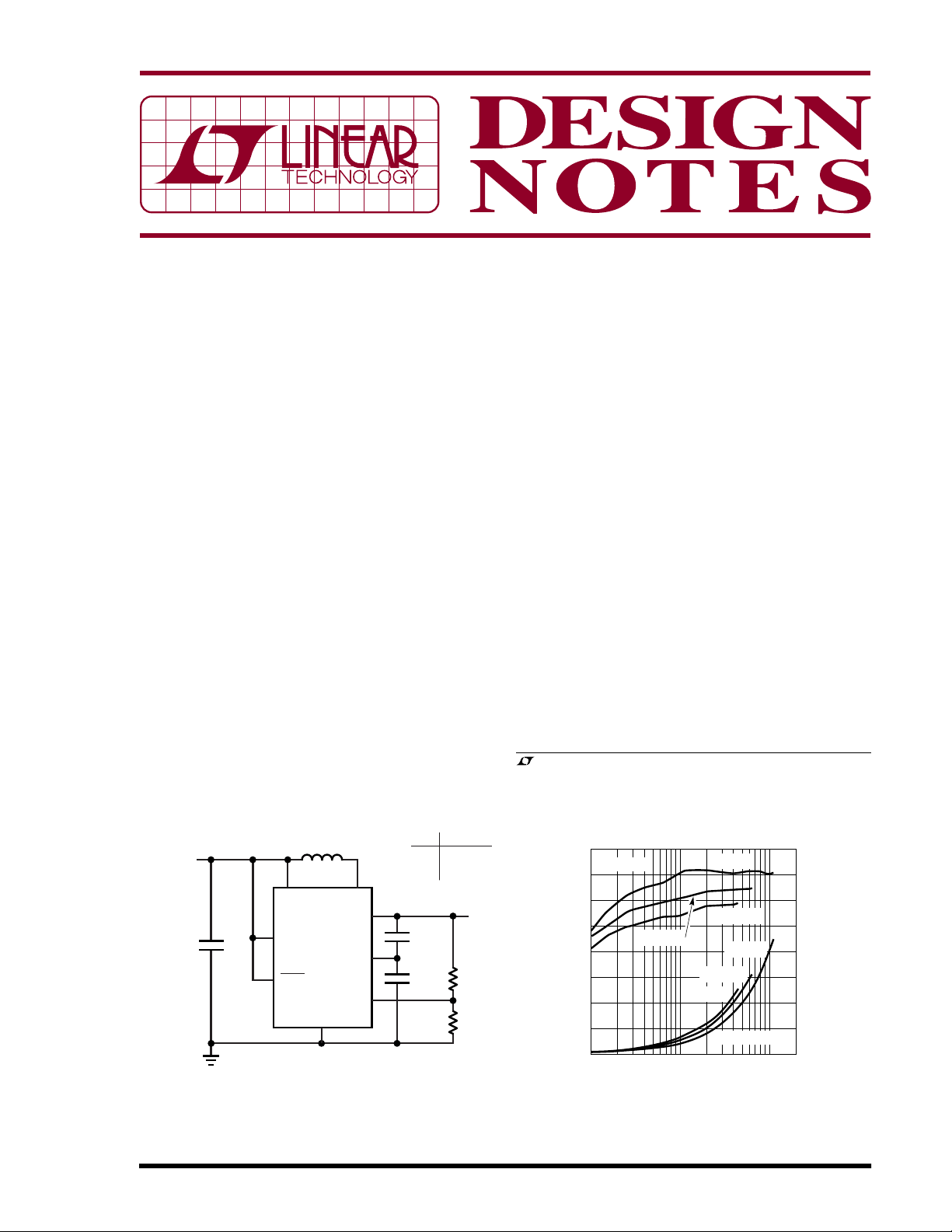
16V Bias Supply
Figure 1 shows a 16V bias supply that can provide 6.5mA
at an efficiency of 77% from a lithium-ion battery (V
=
IN
3.6V) as shown in Figure 2. The circuit uses a 22µH
surface mount chip inductor with a 1210 footprint and a
0.33µF output capacitor with an 0805 footprint. The entire
circuit occupies an area of 51mm
2
. Smaller components
can be used to further reduce the circuit area at the
expense of efficiency. This supply can be used to bias
small LCD panels and small passive organic LED (OLED)
panels as well.
, LTC, LT and Burst Mode are registered trademarks of Linear Technology
Corporation. ThinSOT is a trademark of Linear Technology Corporation.
2.5V TO 6V
03/05/358
L
V
IN
C
IN
1µF
CIN: TAIYO YUDEN LMK107BJ105MA
C
OUT
C
DIS
L: MURATA LQH32CN220K
22µH
V
IN
CTRL
SHDN
: TAIYO YUDEN GMK212BJ334MG
: TAIYO YUDEN EMK107BJ224MA
LT3464
GND
SW
OUT
CAP
FB
C
0.22µF
C
0.33µF
Figure 1. Efficient 16V Bias Supply Using
0805 Output Capacitor and 1210 Choke
V
INIOUT(MAX)
2.5V 4.5mA
3.6V 6.5mA
6V 11mA
DIS
OUT
3.48M
294k
DN358 F01
V
16V
OUT
DN358 F02
80
70
60
POWER LOSS (mW)
50
40
30
20
10
0
85
EFFICIENCY
80
75
70
65
60
EFFICIENCY (%)
55
50
45
0.1
VIN = 6V
VIN = 2.5V
VIN = 3.6V
11020
LOAD CURRENT (mA)
VIN = 6V
VIN = 3.6V
VIN = 2.5V
POWER LOSS
Figure 2. Efficiency and Power Loss of 16V Output
LT3464 Boost Converter (Figure 1 Circuit)
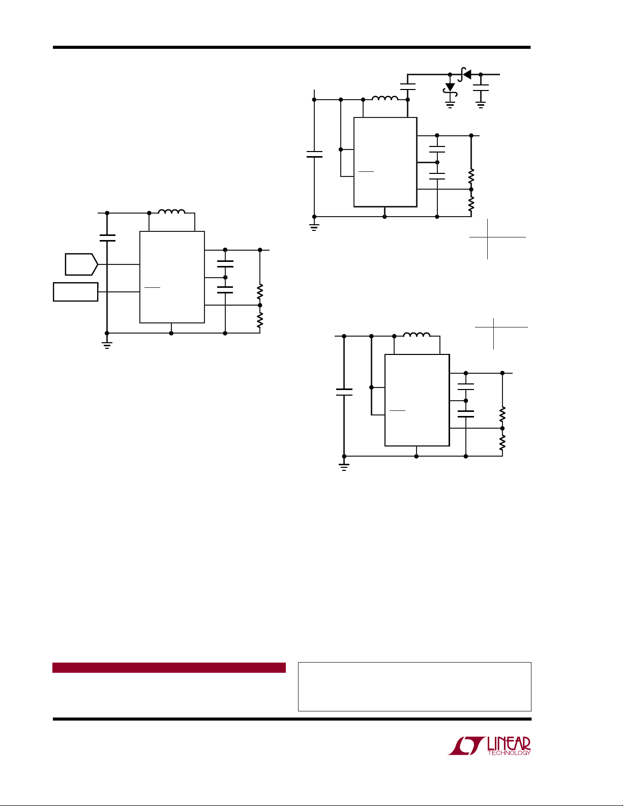
20V Bias Supply with Variable Output Voltage
Manual adjustment of the bias voltage is required in some
LCD applications in order to vary the contrast. The
LT3464 CTRL pin eases this task. When a DC voltage of
1.25V or less is applied to the control pin, the internal
reference is overridden, allowing external control of the
bias voltage from (V
– 0.8V) to nominal V
IN
. Figure 3
OUT
shows a DAC-controlled bias supply. Other methods of
driving the control pin include using a filtered PWM signal
or a potentiometer
V
IN
2.5V TO 6V
DAC
MICRO-
CONTROLLER
Figure 3. 20V Nominal Bias Supply with
DAC Controlled Output Voltage and Shutdown
.
L
22µH
C
1µF
IN
7
V
IN
1
CTRL
LT3464
8
SHDN
GND
CIN: TAIYO YUDEN LMK107BJ105MA
: TAIYO YUDEN GMK212BJ334MG
C
OUT
: TAIYO YUDEN EMK107BJ224MG
C
DIS
L: MURATA LQH32CN220K
6
SW
OUT
CAP
FB
4
3
C
DIS
0.22µF
5
C
OUT
0.33µF
2
V
20V
4.53M
301k
DN358 F03
OUT
±20V Bias Supply
A dual, ±20V bias supply is shown in Figure 4. The +20V
rail is regulated and an inverting charge pump tapped
from its switch node forms a quasi-regulated –20V
output. For a 10:1 difference in load currents, the two
outputs are regulated within 5% of each other. The full
load efficiency is 77% at an input voltage of 3.6V. One
benefit of this circuit is that both outputs are isolated from
the input during shutdown; the positive output is isolated
by the internal disconnect switch and the negative output
is isolated by the charge pump capacitor C
CP
.
34V Bias Supply
The 36V rating of the main switch allows output voltages
up to 34V as illustrated in Figure 5. The 34V bias supply
shown can supply 3.5mA at 76% efficiency from a 3.6V
V
IN
2.5V TO 6V
7
V
IN
1
C
1µF
CIN: TAIYO YUDEN LMK107BJ105MA
C
OUT1
C
OUT2
D1, D2: CENTRAL CMDSH-3
L: MURATA LQH32CN220K
CTRL
IN
8
SHDN
, C
, CCP: TAIYO YUDEN GMK212BJ224MG
DIS
: TAIYO YUDEN GMK316BJ105ML
L
22µH
LT3464
GND
D1
C
CP
0.22µF
6
SW
3
OUT
5
CAP
2
FB
4
C
DIS
0.22µF
C
OUT1
0.22µF
D2
V
OUT
–20V
C
OUT2
1µF
V
OUT
20V
4.53M
301k
I
OUT(MAX)
VINBOTH RAILS
2.5V 1.5mA
3.6V 2.5mA
6V 4mA
DN358 F04
Figure 4. ±20V Bias Supply with
Output Disconnect on Both Rails
V
2.5V TO 6V
L
IN
C
IN
1µF
CIN: TAIYO YUDEN LMK107BJ105MA
C
OUT
C
DIS
L: MURATA LQH32CN470K
47µH
7
V
IN
1
CTRL
LT3464
8
SHDN
GND
: TAIYO YUDEN UMK316BJ474ML
: TAIYO YUDEN GMK212BJ224MG
6
SW
OUT
CAP
FB
4
3
5
2
V
INIOUT(MAX)
2.5V 2.5mA
3.6V 3.5mA
6V 5.5mA
C
DIS
0.22µF
C
OUT
0.47µF
2.61M
100k
DN358 F05
V
34V
OUT
Figure 5. 34V Bias Supply Using the LT3464
input. The 47µH inductor has a 1210 footprint and the
0.47µF output capacitor has a 1206 footprint. The circuit
occupies an area of only 55mm2.
Conclusion
The LT3464 provides a compact, complete solution for
generating high voltage, low current bias supplies.
Data Sheet Download
http://www.linear.com
Linear Technology Corporation
1630 McCarthy Blvd., Milpitas, CA 95035-7417
(408) 432-1900 ● FAX: (408) 434-0507 ● www.linear.com
For applications help,
call (408) 432-1900, Ext. 2759
dn358f LT/TP 0305 409K • PRINTED IN THE USA
© LINEAR TECHNOLOGY CORPORATION 2005
 Loading...