

查询LT3463A供应商
FEATURES
LT3463/LT3463A
Dual Micropower
DC/DC Converters
with Schottky Diodes
U
DESCRIPTIO
■
Generates Well-Regulated Positive and
Negative Outputs
■
Low Quiescent Current:
20µA (per Converter) in Active Mode
<1µA in Shutdown Mode
■
Internal 42V Power Switches
■
Internal 42V Schottky Diodes
■
Low V
■
Input Voltage Range: 2.4V to 15V
■
High Output Voltages: Up to ±40V
■
Low Profile (0.8mm) 3mm x 3mm DFN Package
Switch: 180mV at 150mA
CESAT
U
APPLICATIO S
■
CCD Bias
■
LCD Bias
■
Handheld Computers
■
Digital Cameras
U
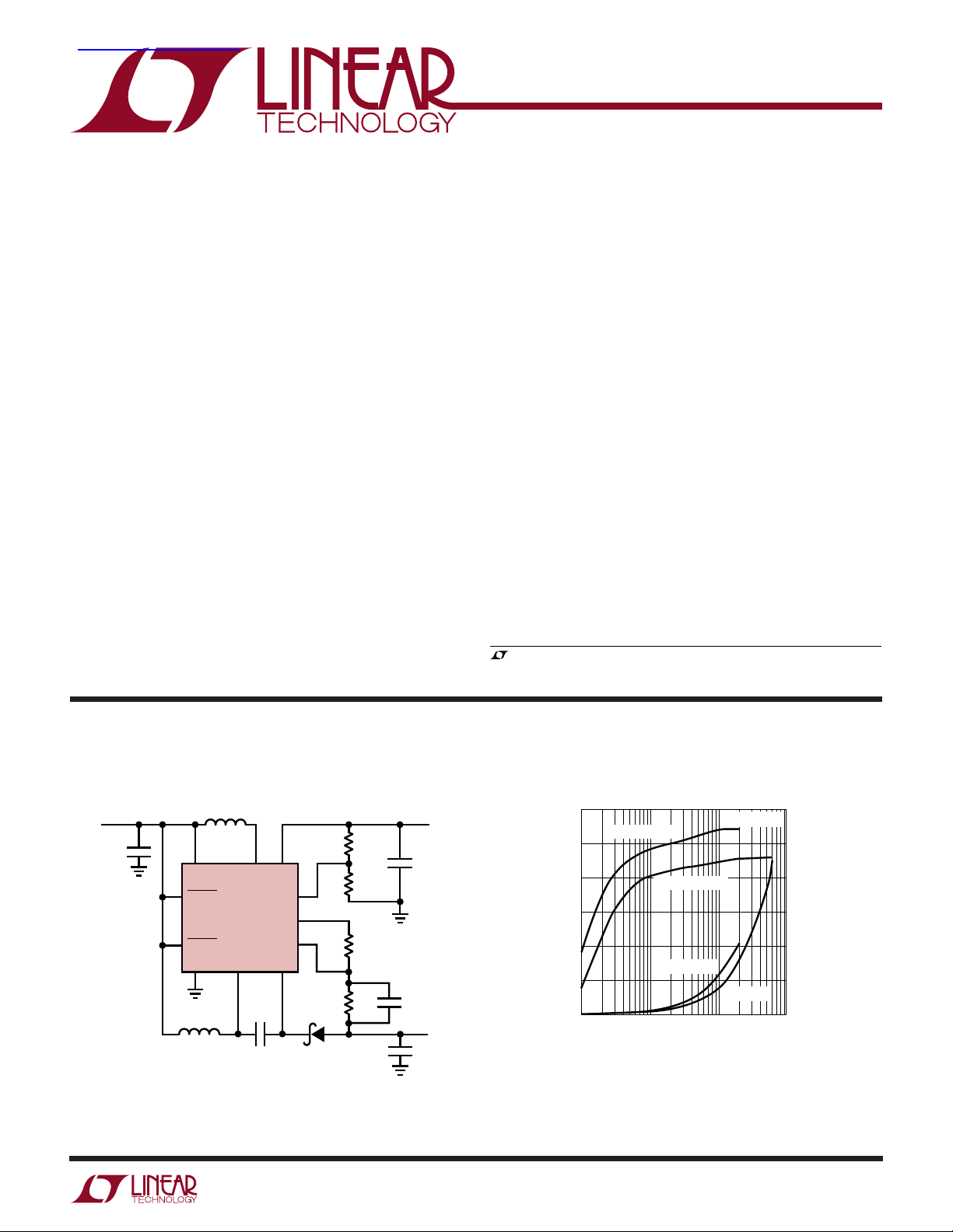
TYPICAL APPLICATIO
The LT®3463/LT3463A are dual micropower DC/DC converters with internal Schottky diodes in a 10-lead 3mm ×
3mm DFN package. Negative and positive LT3463 converters have a 250mA current limit. The LT3463A positive
converter also has a 250mA limit, while the negative
converter has a 400mA limit. Both devices have an input
voltage range of 2.4V to 15V, making them ideal for a wide
variety of applications. Each converter features a quiescent current of only 20µA, which drops to under 1µA in
shutdown. A current limited, fixed off-time control scheme
conserves operating current, resulting in high efficiency
over a broad range of load current. The 42V switch enables
high voltage outputs up to ±40V to be easily generated
without the use of costly transformers. The low 300ns offtime permits the use of tiny, low profile inductors and
capacitors to minimize footprint and cost in space-conscious portable applications.
, LTC and LT are registered trademarks of Linear Technology Corporation.
V
2.7V
TO 5V
IN
4.7µF
CCD Bias Supply (15V, –8V)
10µH
V
IN
SHDN2
GND SW2 D2
10µH
SW1
LT3463A
1µF
V
OUT1
FB1SHDN1
V
REF
FB2
1M
90.9k
154k
1M 10pF
4.7µF
3463 TA01a
2.2µF
V
OUT1
15V
10mA
V
OUT2
–8V
50mA
Efficiency and Power Loss
80
15V EFFICIENCY
75
70
65
EFFICIENCY (%)
60
55
50
0.1
VIN = 3.6V
–8V EFFICIENCY
15V LOSS
–8V LOSS
1 10 100
LOAD CURRENT (mA)
3463 TA01b
240
200
POWER LOSS (mW)
160
120
80
40
0
3463f
1
LT3463/LT3463A
TOP VIEW
DD PACKAGE
10-LEAD (3mm × 3mm) PLASTIC DFN
10
9
6
7
8
4
5
3
2
1
FB1
SHDN1
SHDN2
V
REF
FB2
V
OUT1
SW1
V
IN
SW2
D2
11
ABSOLUTE AXI U RATI GS
(Note 1)
VIN, SHDN1, SHDN2 Voltage ................................... 15V
SW1, SW2, V
D2 Voltage ............................................................. –42V
FB1, FB2 Voltage Range .............................. –0.3V to 2V
Junction Temperature........................................... 125°C
Operating Ambient Temperature Range
(Note 2) .............................................. –40°C to 85°C
Storage Temperature Range ................. –65°C to 125°C
ELECTRICAL CHARACTERISTICS
temperature range, otherwise specifications are at TA = 25°C. VIN = 2.5V, V
PARAMETER CONDITIONS MIN TYP MAX UNITS
Minimum Input Voltage 2.2 2.4 V
Total Quiescent Current For Both Switchers, Not Switching 40 60 µA
Shutdown Current V
V
Pin Voltage With 124kΩ to GND ● 1.23 1.25 1.27 V
REF
V
Pin Voltage Line Regulation With 124kΩ to GND 0.05 0.10 %/V
REF
FB1 Comparator Trip Voltage High to Low Transition ● 1.225 1.25 1.275 V
FB1 Comparator Hysteresis 8mV
FB1 Line Regulation 2.5V < VIN < 15V 0.05 0.10 %/V
FB1 Pin Bias Current (Note 3) V
FB2 Comparator Trip Voltage Low to High Transition ● 0312mV
FB2 Comparator Hysteresis 8mV
FB2 Line Regulation (V
FB2 Pin Bias Current (Note 4) V
SW1 Switch Off Time V
SW2 Switch Off Time V
Switch V
CESAT
Switch Current Limit (SW1) 180 250 320 mA
Switch Current Limit (SW2) LT3463 180 250 320 mA
Swith Leakage Current (SW1, SW2) Switch Off, VSW = 42V 0.01 1 µA
Schottky Forward Voltage (V
Schottky Reverse Leakage Current V
SHDN1 Pin Current V
SHDN2 Pin Current V
SHDN1/SHDN2 Start-Up Threshold 0.3 1 1.5 V
Note 1: Absolute Maximum Ratings are those values beyond which the life
of a device may be impaired.
Note 2: The LT3463/LT3463A are guaranteed to meet performance
specifications from 0°C to 70°C. Specifications over the –40°C to 85°C
2
W
Voltage ....................................... 42V
OUT1
– V
REF
(SW1, SW2) I
) 2.5V < VIN < 15V 0.05 0.10 %/V
FB2
, D2) ID = 150mA 750 mV
OUT1
WW
U
UUW
PACKAGE/ORDER I FOR ATIO
ORDER PART
NUMBER
LT3463EDD
LT3463AEDD
DD PART MARKING
T
= 125°C, θJA = 43°C/W, θJC = 3°C/W
JMAX
EXPOSED PAD (PIN 11) IS GND
AND MUST BE SOLDERED TO PCB
Consult LTC Marketing for parts specified with wider operating temperature ranges.
The ● denotes the specifications which apply over the full operating
= 2.5V unless otherwise noted.
SHDN
= V
SHDN1
= 1.3V ● 20 50 nA
FB1
= –0.1V ● 20 50 nA
FB2
– VIN = 4V 300 ns
OUT1
– VIN = 0V 1.5 µs
V
OUT1
< 0.1V 300 ns
FB2
= 1V 1.5 µs
V
FB2
= 150mA 180 mV
SW
LT3463A 320 400 460 mA
– VSW = 42V 1 5 µA
OUT1
= –42V 1 5 µA
V
D2
= 2.5V 4 10 µA
SHDN1
= 2.5V 4 10 µA
SHDN2
= 0V 0.1 1 µA
SHDN2
operating ambient temperature range are assured by design,
characterization and correlation with statistical process controls.
Note 3: Bias current flows into the FB1 pin.
Note 4: Bias current flows out of the FB2 pin.
LAFC
LBJK
3463f
UW
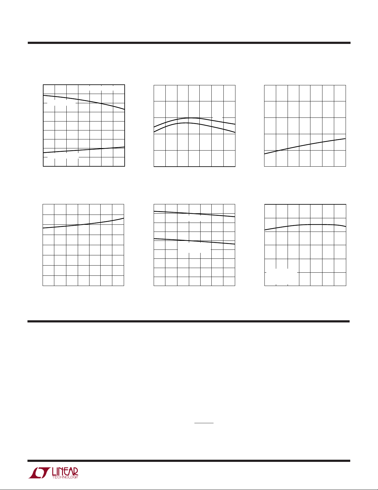
TYPICAL PERFOR A CE CHARACTERISTICS
V
and V
CESAT
900
800
I
700
600
VOLTAGE (V)
500
DIODE
400
300
AND V
200
CESAT
V
100
0
= 150mA
DIODE
I
= 150mA
SWITCH
–50 100
050–25 25 75 125
TEMPERATURE (°C)
Voltage
DIODE
FOR BOTH SWITCHERS
3463 G01
V
and V
REF
1.27
1.26
1.25
VOLTAGE (V)
FB1
1.24
AND V
REF
V
1.23
1.22
–50 100
Voltage V
FB1
V
FB1
050–25 25 75 125
TEMPERATURE (°C)
V
REF
3463 G02
LT3463/LT3463A
Voltage
FB2
10
8
6
4
VOLTAGE (mV)
FB2
V
2
0
–50 25 75
–25 0
TEMPERATURE (°C)
50 100 125
3463 G03
Switch Off Time
400
350
300
250
200
150
SWITCH OFF TIME (ns)
100
50
0
–50
050
–25 25 75 125
100
TEMPERATURE (°C)
3463 G04
Switch Current Limit
450
400
350
300
250
200
150
100
SWITCH CURRENT LIMIT (mA)
50
0
–25 25 75 125
–50
LT3463A SW2
LT3463 SW1, SW2
LT3463A SW1
050
TEMPERATURE (°C)
UUU
PI FU CTIO S
V
(Pin 1): Output Voltage Switcher 1. This is the
OUT1
cathode of an internal Schottky diode whose anode is
connected to the SW1 pin.
Quiescent Current
60
50
40
30
20
QUIESCENT CURRENT (µA)
NOT SWITCHING
10
= 1.3V
V
FB1
V
= –0.1V
FB2
100
3463 G05
0
–50
–25 0
50 100 125
25 75
TEMPERATURE (°C)
3463 G06
D2 (Pin 5): Diode for Switcher 2. This is the anode of an
internal Schottky diode whose cathode connected to the
GND pin.
SW1 (Pin 2): Switch Pin for Switcher 1. This is the
collector of the internal NPN switch. Minimize the metal
trace area connected to this pin to minimize EMI.
VIN (Pin 3): Input Supply Pin. Bypass this pin with a
capacitor as close to the device as possible.
SW2 (Pin 4): Switch Pin for Switcher 2. This is the
collector of the internal NPN switch. Minimize the metal
trace area connected to this pin to minimize EMI.
FB2 (Pin 6): Feedback Pin for Switcher 2. Set the output
voltage by selecting values for R3 and R4.
V
(Pin 7): Voltage Reference Pin (1.25V). This pin is
REF
used along with FB2 to set the negative output voltage for
Switcher 2.
SHDN2 (Pin 8): Shutdown Pin for Switcher 2. Pull this pin
above 1.5V to enable Switcher 2. Pull below 0.3V to turn
it off. Do not leave this pin floating.
3463f
3

LT3463/LT3463A
U
UU
PI FU CTIO S
SHDN1 (Pin 9): Shutdown Pin for Switcher 1. Pull this pin
above 1.5V to enable Switcher 1. Pull below 0.3V to turn
it off. Do not leave this pin floating.
FB1 (Pin 10): Feedback Pin for Switcher 1. Set the output
voltage by selecting values for R1 and R2.
W
BLOCK DIAGRA
V
OUT1
V
IN
C1
3
V
IN
9
SHDN1SHDN1
L1
300ns
ONE-SHOT
V
2
SW1
OUT1
V
OUT2
C2
C3
1
V
OUT1
D1
Q1
GND (Pin 11): Exposed Pad. Solder this exposed pad
directly to the local ground plane. This pad must be
electrically connected for proper operation.
C4
D3
5
D2
D2
L2
V
IN
4
SW2
8
Q2
300ns
ONE-SHOT
1.25V
V
REF
7
SHDN2SHDN2
R2
FB1
10
R1
LT3463: R
LT3463A: R
–
+
= RS2 = 0.1Ω
S1
= 0.1Ω, RS2 = 0.063Ω
S1
A2A1
SWITCHER 1
+
R
S1
–
25mV
Figure 1. Block Diagram
U
OPERATIO
The LT3463 uses a constant off-time control scheme to
provide high efficiency over a wide range of output current. Operation can be best understood by referring to the
block diagram in Figure 1. When the voltage at the FB1 pin
is slightly above 1.25V, comparator A1 disables most of
the internal circuitry. Output current is then provided by
capacitor C2, which slowly discharges until the voltage at
the FB1 pin goes below the hysteresis point of A1 (typical
hysteresis at the FB1 pin is 8mV). A1 then enables the
internal circuitry, turns on power switch Q1, and the
FB2
+
+
R
S2
25mV1.25V
GND
11
–
A4 A3
SWITCHER 2
6
–
3463 F01
V
OUT2
current in inductor L1 begins ramping up. Once the switch
current reaches 250mA, comparator A2 resets the oneshot, which turns off Q1 for 300ns. Q1 turns on again and
the inductor currents ramp back up to 250mA, then A2
again resets the one-shot. This switching action continues
until the output voltage is charged up (until the FB1 pin
reaches 1.25V), then A1 turns off the internal circuitry and
the cycle repeats. The second switching regulator is an
inverting converter (which generates a negative output)
but the basic operation is the same.
R3
R4
4
3463f

LT3463/LT3463A
L
VV
I
t
OUT D
LIM
OFF
=
+
2
U
WUU
APPLICATIO S I FOR ATIO
Choosing an Inductor
Several recommended inductors that work well with the
LT3463 are listed in Table 1, although there are many other
manufacturers and devices that can be used. Consult each
manufacturer for more detailed information and for their
entire selection of related parts. Many different sizes and
shapes are available. Use the equations and recommendations in the next few sections to find the correct inductance
value for your design.
Table 1. Recommended Inductors
MAX MAX HEIGHT
µ
PART L (
CMD4D06 4.7 750 0.22 0.8 Sumida
CDRH3D16 10 500 0.19 1.8 Sumida
LPO4812 4.7 600 0.16 1.2 Coilcraft
LQH32C 10 450 0.39 1.8 Murata
LQH31C 4.7 340 0.85 1.8 Murata
Inductor Selection—Boost Regulator
The formula below calculates the appropriate inductor
value to be used for a boost regulator using the LT3463 (or
at least provides a good starting point). This value provides a good tradeoff in inductor size and system performance. Pick a standard inductor close to this value. A
larger value can be used to slightly increase the available
output current, but limit it to around twice the value
calculated below, as too large of an inductance will increase the output voltage ripple without providing much
additional output current. A smaller value can be used
(especially for systems with output voltages greater than
12V) to give a smaller physical size. Inductance can be
calculated as:
VV V
OUT
L
=
where VD = 0.5V (Schottky diode voltage), I
(or 400mA) and t
H) IDC (mA) DCR(Ω) (mm) MANUFACTURER
10 500 0.46 (847) 956-0666
22 310 1.07 www.sumida.com
22 310 0.36
10 400 0.30 (847) 639-6400
22 280 0.64 www.coilcraft.com
15 300 0.75 (714) 852-2001
22 250 0.92 www.murata.com
−+
IN MIN
()
I
LIM
= 300ns; for designs with varying V
OFF
D
t
OFF
= 250mA
LIM
IN
such as battery powered applications, use the minimum
VIN value in the above equation. For most regulators with
output voltages below 7V, a 4.7µH inductor is the best
choice, even though the equation above might specify a
smaller value.
For higher output voltages, the formula above will give
large inductance values. For a 3V to 20V converter (typical
LCD Bias application), a 21µH inductor is called for with
the above equation, but a 10µH inductor could be used
without much reduction in the maximum output current.
Inductor Selection—Inverting Regulator
The formula below calculates the appropriate inductor
value to be used for an inverting regulator using the
LT3463 (or at least provides a good starting point). This
value provides a good tradeoff in inductor size and system
performance. Pick a standard inductor close to this value
(both inductors should be the same value). A larger value
can be used to slightly increase the available output
current, but limit it to around twice the value calculated
below, as too large of an inductance will increase the
output voltage ripple without providing much additional
output current. A smaller value can be used (especially for
systems with output voltages greater than 12V) to give a
smaller physical size. Inductance can be calculated as:
where VD = 0.5V (Schottky diode voltage), I
(or 400mA) and t
= 300ns.
OFF
= 250mA
LIM
For higher output voltages, the formula above will give
large inductance values. For a 3V to 20V converter (typical
LCD bias application), a 49µH inductor is called for with
the above equation, but a 10µH or 22µH inductor could be
used without much reduction in the maximum output
current.
Inductor Selection—Inverting Charge Pump Regulator
For the inverting regulator, the voltage seen by the internal
power switch is equal to the sum of the absolute value of
the input and output voltages, so that generating high
3463f
5

LT3463/LT3463A
VV
R
R
VV
R
R
OUT
OUT12
125 1
2
1
125
4
3
=+
=
.
–.
U
WUU
APPLICATIO S I FOR ATIO
output voltages from a high input voltage source will often
exceed the 50V maximum switch rating. For instance, a
12V to – 40V converter using the inverting topology would
generate 52V on the SW pin, exceeding its maximum
rating. For this application, an inverting charge pump is
the best topology.
The formula below calculates the approximate inductor
value to be used for an inverting charge pump regulator
using the LT3463. As for the boost inductor selection, a
larger or smaller value can be used. For designs with
varying VIN such as battery powered applications, use the
minimum VIN value in the equation below.
VV V
−+
OUT
L
=
Capacitor Selection
The small size and low ESR of ceramic capacitors makes
them ideal for LT3463 applications. Use only X5R and X7R
types because they retain their capacitance over wider
voltage and temperature ranges than other ceramic types.
A 1µF input capacitor and a 0.22µF or 0.47µF output
capacitor are sufficient for most applications. Table 2
shows a list of several ceramic capacitor manufacturers.
Consult the manufacturers for more detailed information
on their entire selection of ceramic capacitors. For applications needing very low output voltage ripple, larger
output capacitor values can be used.
IN MIN
()
I
LIM
D
t
OFF
inrush current include a larger more abrupt voltage step at
VIN, a larger output capacitor tied to the outputs, and an
inductor with a low saturation current.
While the internal diode is designed to handle such events,
the inrush current should not be allowed to exceed 1 amp.
For circuits that use output capacitor values within the
recommended range and have input voltages of less than
5V, inrush current remains low, posing no hazard to the
device. In cases where there are large steps at VIN and/or
a large capacitor is used at the outputs, inrush current
should be measured to ensure safe operation.
Setting the Output Voltages
The output voltages are programmed using two feedback
resistors. As shown in Figure 1, resistors R1 and R2
program the positive output voltage (for Switcher 1), and
resistors R3 and R4 program the negative output voltage
(for Switcher 2) according to the following formulas:
R1 and R3 are typically 1% resistors with values in the
range of 50k to 250k.
Board Layout Considerations
Table 2. Recommended Ceramic Capacitor Manufacturers
MANUFACTURER PHONE URL
AVX 843-448-9411 www.avxcorp.com
Kemet 408-986-0424 www.kemet.com
Murata 814-237-1431 www.murata.com
Taiyo Yuden 408-573-4150 www.t-yuden.com
Inrush Current
When VIN is increased from ground to operating voltage
while the output capacitor is discharged, an inrush current
will flow through the inductor and integrated Schottky
diode into the output capacitor. Conditions that increase
6
As with all switching regulators, careful attention must be
paid to the PCB board layout and component placement.
To maximize efficiency, switch rise and fall times are made
as short as possible. To prevent electromagnetic interference (EMI) problems, proper layout of the high frequency
switching path is essential. The voltage signal of the SW
pin has sharp rising and falling edges. Minimize the length
and area of all traces connected to the SW pin and always
use a ground plane under the switching regulator to
minimize interplane coupling. In addition, the ground
connection for the feedback resistor R1 should be tied
directly to the GND pin and not shared with any other
component, ensuring a clean, noise-free connection.
3463f

TYPICAL APPLICATIO
V
IN
2.7V
TO 5V
PACKAGE DESCRIPTIO
U
1µF
LT3463/LT3463A
Dual Output ±20V Converter
L1
10µH
C1
321
V
SW1
OUT1
10
FB1
LT3463
SW2
11
4
C4
0.1µF
7
V
REF
6
FB2
D2
5
9
8
V
IN
SHDN1
SHDN2
GND
L2
10µH
R2
1M
R1
66.5k
R3
61.9k
R4
1M
D1
C3
0.47µF
C2
0.47µF
3463 TA02
V
OUT1
20V
9mA
V
OUT2
–20V
9mA
U
10-Lead Plastic DFN (3mm × 3mm)
(Reference LTC DWG # 05-08-1699)
0.675 ±0.05
3.50 ±0.05
NOTE:
1. DRAWING TO BE MADE A JEDEC PACKAGE OUTLINE M0-229 VARIATION OF (WEED-2).
CHECK THE LTC WEBSITE DATA SHEET FOR CURRENT STATUS OF VARIATION ASSIGNMENT
2. DRAWING NOT TO SCALE
3. ALL DIMENSIONS ARE IN MILLIMETERS
4. DIMENSIONS OF EXPOSED PAD ON BOTTOM OF PACKAGE DO NOT INCLUDE
MOLD FLASH. MOLD FLASH, IF PRESENT, SHALL NOT EXCEED 0.15mm ON ANY SIDE
1.65 ±0.05
(2 SIDES)2.15 ±0.05
PACKAGE
OUTLINE
0.25 ± 0.05
2.38 ±0.05
RECOMMENDED SOLDER PAD PITCH AND DIMENSIONS
(2 SIDES)
0.50
BSC
TOP MARK
(SEE NOTE 6)
DD Package
PIN 1
0.200 REF
R = 0.115
TYP
3.00 ±0.10
(4 SIDES)
0.75 ±0.05
5. EXPOSED PAD SHALL BE SOLDER PLATED
6. SHADED AREA IS ONLY A REFERENCE FOR PIN 1 LOCATION ON THE
TOP AND BOTTOM OF PACKAGE
1.65 ± 0.10
(2 SIDES)
0.00 – 0.05
2.38 ±0.10
(2 SIDES)
BOTTOM VIEW—EXPOSED PAD
106
15
0.25 ± 0.05
0.50 BSC
0.38 ± 0.10
(DD10) DFN 1103
Information furnished by Linear Technology Corporation is believed to be accurate and reliable.
However, no responsibility is assumed for its use. Linear Technology Corporation makes no representation that the interconnection of its circuits as described herein will not infringe on existing patent rights.
3463f
7

LT3463/LT3463A
TYPICAL APPLICATIO
2.7V
TO 5V
U
CCD Bias Supply
L1
V
IN
C1
4.7µF
C1: TAIYO YUDEN JMK212BJ475MG
C2: TAIYO YUDEN EMK316BJ225ML
C3: TAIYO YUDEN LMK316BJ475ML
C4: TAIYO YUDEN EMK212BJ105MG
C5: AVX 06035A100KAT2A
D1: DIODES, INC B0540W
L1, L2: MURATA LQH32CN100K53
10µH
321
V
11
SW1
LT3463A
SW2
4
C4
1µF
OUT1
FB1
V
REF
FB2
D2
9
8
V
IN
SHDN1
SHDN2
GND
L2
10µH
R2
1M
10
7
6
5
R1
90.9k
R3
154k
R4
1M
D1
C3
4.7µF
C2
2.2µF
C5
10pF
3463 TA01a
V
OUT1
15V
10mA
V
OUT2
–8V
50mA
Typical Waveforms for 15V Output Typical Waveforms for –8V Output
V
V
SW1
10V/DIV
V
OUT1
AC-COUPLED
50mV/DIV
200mA/DIV
I
L1
2µs/DIV
3463 TA04
SW2
5V/DIV
V
OUT2
AC-COUPLED
50mV/DIV
I
200mA/DIV
L2
RELATED PARTS
PART NUMBER DESCRIPTION COMMENTS
LT1615/LT1615-1 300mA/80mA (ISW), High Efficiency Step-Up DC/DC Converters VIN: 1V to 15V, V
ThinSOT Package
LT1944 Dual Output 350mA (ISW), Constant Off-Time, VIN: 1.2V to 15V, V
High Efficiency Step-Up DC/DC Converter MS Package
LT1944-1 Dual Output 150mA (ISW), Constant Off-Time, VIN: 1.2V to 15V, V
High Efficiency Step-Up DC/DC Converter MS Package
LT1945 Dual Output, Pos/Neg, 350mA (ISW), VIN: 1.2V to 15V, V
Constant Off-Time, High Efficiency Step-Up DC/DC Converter MS Package
LT3464 85mA (ISW), High Efficiency Step-Up DC/DC Converter VIN: 2.3V to 10V, V
with Integrated Schottky and PNP Disconnect ThinSOT Package
OUT(MAX)
2µs/DIV
: 34V, IQ: 20µA, ISD: <1µA,
: 34V, IQ: 20µA, ISD: <1µA,
OUT(MAX)
: 34V, IQ: 20µA, ISD: <1µA,
OUT(MAX)
: ±34V, IQ: 20µA, ISD: <1µA,
OUT(MAX)
: 34V, IQ: 25µA, ISD: <1µA,
OUT(MAX)
3463 TA05
8
Linear Technology Corporation
1630 McCarthy Blvd., Milpitas, CA 95035-7417
(408) 432-1900 ● FAX: (408) 434-0507
●
www.linear.com
3463f
LT/TP 0404 1K • PRINTED IN USA
LINEAR TECHNOLOGY CORPORATION 2003
 Loading...