

查询LT3439供应商
FEATURES
■
Reduced Conducted and Radiated EMI
■
Single Resistor Control of Output Switch Voltage
and Current Slew Rates
■
Cross Conduction Prevention Circuitry
■
Two 1A Current Limited Power Switches
■
Low Minimum Supply Voltage: 2.8V
■
Low Shutdown Current: <20µA
■
50% Duty Cycle
■
20kHz to 250kHz Oscillator Frequency
■
Synchronizable to 300kHz
■
Overcurrent and Overtemperature Protected
U
APPLICATIO S
■
Low Noise Isolated Supplies
■
Radio and Telecom Supplies
■
Distributed Supplies
■
Medical Instruments
■
Precision Instruments
■
Low Noise Filament Supplies
LT3439
Slew Rate Controlled
Ultralow Noise1A Isolated
DC/DC Transformer Driver
U
DESCRIPTIO
The LT®3439 is a push-pull DC/DC transformer driver that
reduces conducted and radiated electromagnetic interference (EMI). Ultralow noise and EMI are achieved by
controlling the output switch voltage and current slew
rates. Slew rates are user adjustable to optimize output
noise versus efficiency. The LT3439 can reduce high
frequency harmonic content by as much as 40dB with only
a minor decrease in efficiency.
The LT3439 includes two 1A current limited power switches
to ensure start-up under heavy loads. It also includes an
oscillator that can be synchronized to an external clock for
more accurate placement of switcher harmonics. Protection features include current limiting, undervoltage lockout, thermal shutdown and cross conduction prevention
circuitry.
The LT3439 is available in a thermally enhanced 16-pin
TSSOP with an exposed backside.
, LTC and LT are registered trademarks of Linear Technology Corporation.
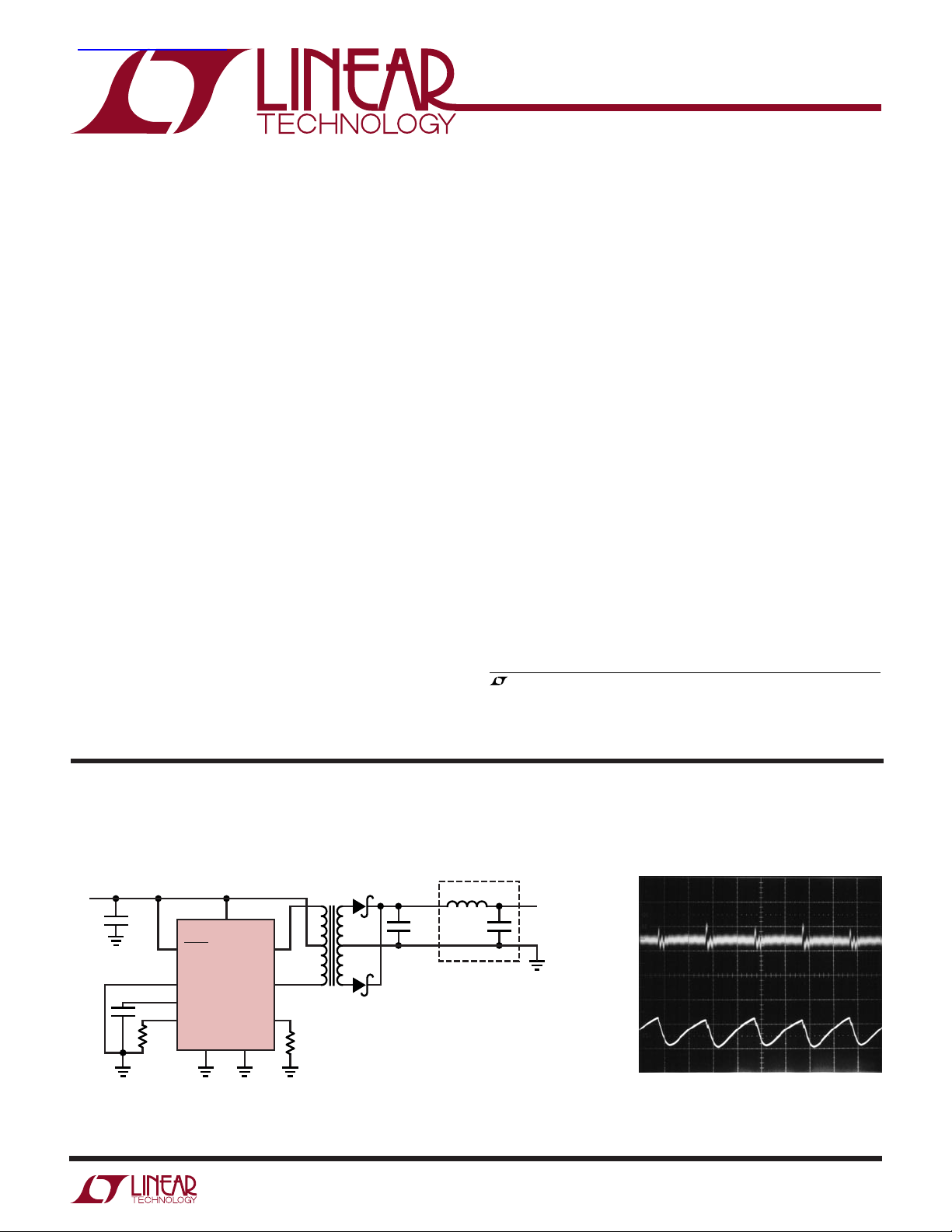
TYPICAL APPLICATIO
Low Noise 5V to 5V Push-Pull DC/DC Transformer
V
IN
5V
C
IN
22µF
10V
680pF
16.9k
11
5
6
V
SHDN
LT3439
SYNC
C
T
R
T
GND PGND
10
13
IN
COL A
COL B
R
1, 16
3
14
47
SL
34k
3439 TA01
U
OPTIONAL
D1
T1
•
•
•
•
A
D2
C
C1, C2: TDK C4532X5R0J476M
D1, D2: MBR0520
L1: TDK SLF6028T-330MR69
T1: COILTRONICS 15835
L1 33µH
C1
47µF
6.3V
: MURATA GRM235Y5V226Z10
IN
47µF
6.3V
B
C2
V
OUT
5V
500mA
200µV/DIV
20mV/DIV
B
A
5V Output Noise
5µs/DIV 3439 TA01b
sn3439 3439fs
1
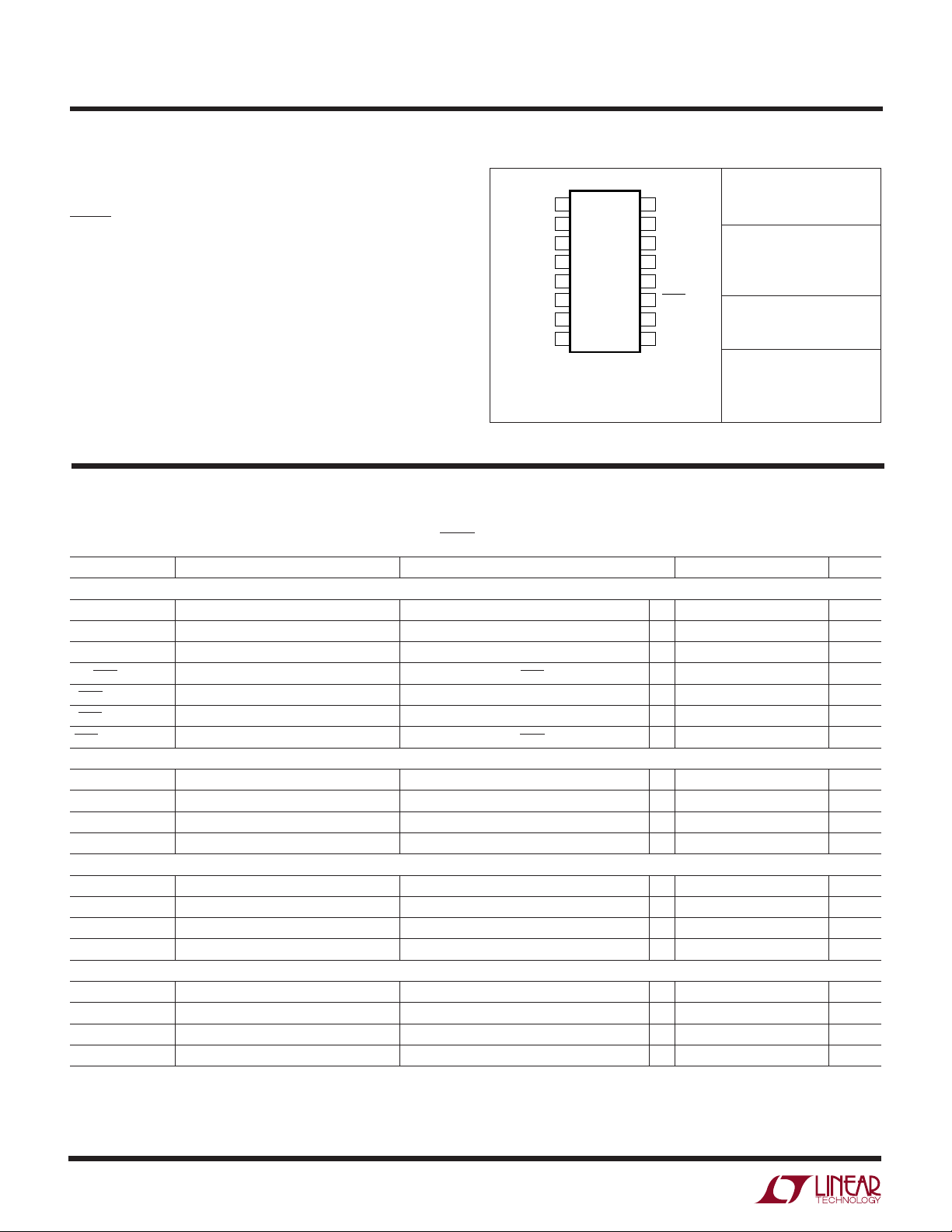
LT3439
FE PACKAGE
16-LEAD PLASTIC TSSOP
1
2
3
4
5
6
7
8
TOP VIEW
16
15
14
13
12
11
10
9
PGND
NC
COL A
R
SL
SYNC
C
T
R
T
NC
PGND
NC
COL B
V
IN
NC
SHDN
GND
NC
WWWU
ABSOLUTE AXI U RATI GS
PACKAGE/ORDER I FOR ATIO
UU
W
(Note 1)
VIN Voltage ............................................................. 20V
COL A, COL B Voltage............................................. 35V
ORDER PART
NUMBER
SHDN, SYNC Voltage.............................................. 20V
Maximum Junction Temperature ......................... 150°C
LT3439EFE
Operating Junction Temperature Range
(Note 2) ............................................ –40°C to 125°C
Storage Temperature Range ................ –65°C to 150°C
Lead Temperature (Soldering, 10 sec)................. 300°C
FE PART
MARKING
3439EFE
T
= 125°C, θJA = 40°C/W
JMAX
NOTE: BACKSIDE OF PACKAGE CONNECTED TO GND
Consult LTC Marketing for parts specified with wider operating temperature ranges.
ELECTRICAL CHARACTERISTICS
The ● denotes specifications which apply over the full operating temperature range, otherwise specifications are at TA = 25°C.
VIN = 5V; RT = 16.9k; CT = 680pF; RSL = 16.9k; COL A, COL B, SHDN pins open, unless otherwise noted.
SYMBOL PARAMETER CONDITIONS MIN TYP MAX UNITS
Supply and Shutdown
V
IN
V
IN(MIN)
I
VIN
I
VIN(SHDN)
V
SHDN(ON)
V
SHDN(OFF)
I
SHDN
Oscillator and Sync
f
MAX
f
SYNC
V
SYNC
R
SYNC
Output Switches (COL A, COL B)
DC Switch Duty Cycle ● 50 %
BV Output Switch Breakdown Voltage 2.8V ≤ VIN ≤ 17.5V ● 35 50 V
R
ON
I
LIM(MAX)
Slew Control
V
SLEWR
V
SLEWF
I
SLEWR
SLEWF
I
Note 1: Absolute Maximum Ratings are those values beyond which the life
of a device may be impaired.
Operating Range ● 2.8 17.5 V
Minimum Input Voltage 2.55 2.7 V
Supply Current 2.8V ≤ VIN ≤ 17.5V ● 12 mA
Supply Current in Shutdown Mode 2.8V ≤ VIN ≤ 17.5V, V
= 0V 5 20 µA
SHDN
Shutdown Turn-On Threshold 2.8V ≤ VIN ≤ 17.5V ● 1.3 1.4 V
Shutdown Turn-Off Threshold 2.8V ≤ VIN ≤ 17.5V ● 1.20 1.26 V
Shutdown Pin Current Hysteresis 2.8V ≤ VIN ≤ 17.5V, V
= 1.4V ● 10 20 40 µA
SHDN
Oscillator Frequency ● 250 kHz
Synchronization Frequency Range ● 300 kHz
SYNC Pin Threshold ● 1.4 2.25 V
SYNC Pin Input Resistance 40 kΩ
Output Switch On Resistance I
COLA
or I
= 0.75A ● 0.5 0.95 Ω
COLB
Switch Current Limit 1.2 1.4 1.65 A
Output Voltage Slew Rising Edge Collector A or B 17 V/µs
Output Voltage Slew Falling Edge Collector A or B 17 V/µs
Output Current Slew Rising Edge Collector A or B 5 A/µs
Output Current Slew Falling Edge Collector A or B 5 A/µs
Note 2: The LT3439E is guaranteed to meet performance specifications
from 0°C to 70°C. Specifications over the –40°C to 125°C operating
junction temperature range are assured by design, characterization and
correlation with statistical process controls.
sn3439 3439fs
2
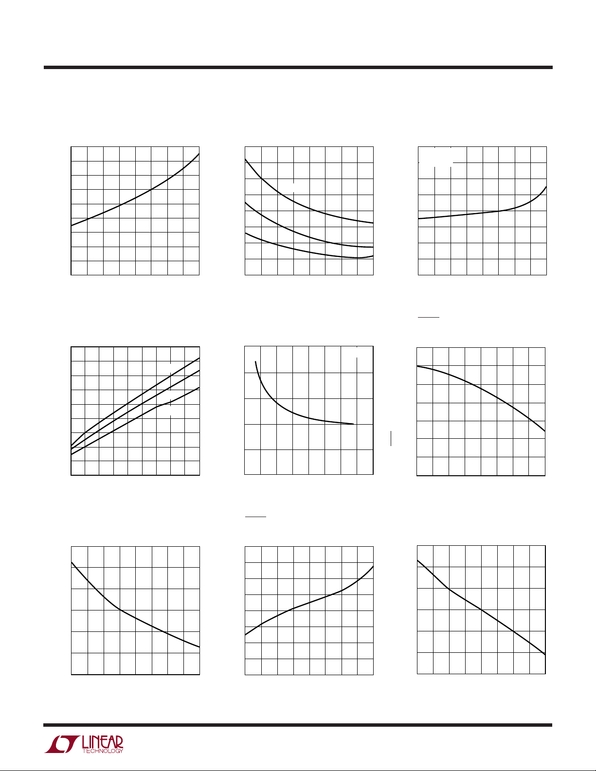
UW
TEMPERATURE (°C)
–50
1.0
VOLTAGE THRESHOLD (V)
1.1
1.2
1.3
1.4
050
100
150
3439 G09
1.5
1.6
–25 25
75
125
TEMPERATURE (°C)
–50
SHDN PIN CURRENT (µA)
18
20
22
25
3439 G06
16
14
–25 0 15050 75 100 125
12
10
24
TYPICAL PERFOR A CE CHARACTERISTICS
LT3439
Minimum Input Voltage
vs Temperature
2.750
2.700
2.650
2.600
2.550
2.500
2.450
INPUT VOLTAGE (V)
2.400
2.350
2.300
–50
–25
0
TEMPERATURE (°C)
Switch Voltage Drop
vs Switch Current
0.9
0.8
0.7
0.6
0.5
0.4
0.3
SWITCH VOLTAGE (V)
0.2
0.1
0
0.1 0.2 0.3
0.4 0.5 0.6 1.0
SWITCH CURRENT (A)
25 50 75 100
125°C
85°C
25°C
0.7 0.8 0.9
125 150
3439 G01
3439 G04
Supply Current in Shutdown Mode
vs Temperature
16
14
12
10
8
6
SUPPLY CURRENT (µA)
4
2
0
–50
–25
0
17.5V
5V
2.7V
25 50 75 100
TEMPERATURE (°C)
Supply Current vs Slew Resistor
25
20
15
10
SUPPLY CURRENT (mA)
5
0
10000
0
20000
SLEW RESISTOR (Ω)
30000
125 150
3439 G02
TA = 25°C
3439 G05
40000
Oscillator Frequency
vs Temperature
120
RT = 16.9k
= 680pF
C
T
115
110
105
100
95
90
OSCILLATOR FREQUENCY (kHz)
85
80
–50
–25
0
25 50 75 100
TEMPERATURE (°C)
SHDN Pin Hysteresis Current
vs Temperature
125 150
3439 G03
2.0
1.8
1.6
1.4
1.2
CURRENT LIMIT (A)
1.0
0.8
–50
Current Limit vs Temperature
50
–25 0
25 75 150
TEMPERATURE (°C)
100 125
3439 G07
SHDN Pin Voltage Threshold
vs Temperature
1.35
1.34
1.33
1.32
1.31
1.30
1.29
THRESHOLD VOLTAGE (V)
1.28
1.27
–50
–25
0
25 50 75 100
TEMPERATURE (°C)
SYNC Pin Voltage Threshold
vs Temperature
125 150
3439 G08
sn3439 3439fs
3

LT3439
U
UU
PI FU CTIO S
PGND (Pins 1, 16): Power ground is connected to the
emitter of the power switches via an internal sense resistor. It has large currents flowing through it and should be
connected to a good quality ground plane.
COL A, COL B (Pins 3, 14): These are the open collectors
of the output power switches. They are connected to the
outer terminals of the center tap transformer. Large currents flow into these pins so external traces should be kept
as short as possible.
RSL (Pin 4): The slew control resistor sets the maximum
current and voltage slew rate for the collectors A and B.
The minimum resistor value is 3.4k for fast slewing and the
maximum resistor is 34k for slow slewing. For more
details, see “Slew Rate Setting” in the Applications Information section of this data sheet.
SYNC (Pin 5): The SYNC pin can be used to synchronize
the oscillator to an external clock. RT and CT should be set
such that the oscillator clock frequency is approximately
10% below the external clock frequency. If unused, this
pin should be tied to GND. For more details, see “Oscillator
Sync” in the Applications Information section of this data
sheet.
CT (Pin 6): The oscillator capacitor pin is used in conjunction with the RT pin to set the oscillator frequency. For
RT = 16.9k, CT can be calculated as follows:
CT(nF) = 70/f
OSC
(kHz)
RT (Pin 7): The oscillator resistor pin is used to set the
charge and discharge currents of the oscillator capacitor.
The nominal value is 16.9k. The resistance can be adjusted
between ±25% of nominal for better frequency accuracy.
SHDN (Pin 11): The SHDN pin is used to shut down the
part. Grounding this pin will disable all internal circuitry.
Increasing the SHDN voltage above the turn-on threshold
will enable the part. At the turn-on threshold, approximately 20µA of current is sourced out of the pin. This
current, in conjunction with the Thevenin resistance on the
pin, sets up the hysteresis. This allows the user to set the
undervoltage lockout (UVLO) of the supply and the amount
of start-up hysteresis with a resistor divider off of the input
voltage. Above 2.1V on the SHDN pin, the hysteresis
current is reduced to zero. If unused the pin can be left
floating or tied directly to the input voltage.
GND (Pin 10): Signal Ground. The oscillator, slew control
circuitry and the internal regulator are referred to signal
ground. Internally, signal ground is tied to substrate and
the exposed backside of the device. Connect the GND pin
to the ground plane and keep the connection free of large
currents.
VIN (Pin 13): This is the supply pin for the part and should
be bypassed with a 4.7µF or greater, low ESR capacitor.
When VIN ≤ 2.5V, an internal undervoltage lockout circuit
will trip and turn both outputs off.
The transformer operating frequency and the frequency
of each output is one half of the frequency of the oscillator.
4
sn3439 3439fs

BLOCK DIAGRA
LT3439
W
D1
T1
14
PGND
•••
•
16
1
3439 BD
V
IN
31311
SHDN V
IN
LDO
REGULATOR
T
R
T
7
C
T
6
5
R
T
C
T
SYNC
INTERNAL V
OSCILLATOR
CC
LT3439
Q
GND
SLEW
CONTROL
R
SL
4
R
SL
FF
QB
10
COLA
+
–
COLB
OUTPUT
DRIVERS
R
SENSE
V
OUT
C
OUT
D2
U
OPERATIO
Push-Pull Topology
The push-pull DC transformer topology is a very straightforward switching power supply. The two switches are
turned on out of phase at 50% duty cycles. During the
switch on time, VIN is applied across the primary side of
the transformer. The voltage on the secondary side of the
transformer is simply VIN times the turns ratio. The diodes
rectify the secondary voltage and generate the output
voltage. The output capacitor is for hold-up and filtering.
Some of the topology’s advantages are: 1) Stepping up or
down the input voltage can easily be done by setting the
turns ratio. 2) The transformer provides isolation between
the input and output. 3) Each switch cycle applies V
across the transformer in opposite polarities. Therefore,
the transformer core never saturates and a separate reset
circuit is not necessary.
The push-pull topology is not without its concerns. An
imbalance in the two sides of the transformer can
IN
eventually cause the transformer to saturate. Also, during the turn-off of the switches, the leakage inductance
causes a large undesirable voltage spike. The LT3439
slew control feature addresses both of these concerns
and is discussed in the Applications Information section.
Slew Control
Control of voltage and current slew rate is maintained via
two feedback loops. One loop controls the output switch
collector voltage dV/dt and the other loop controls the
emitter current dI/dt. Output slew control is achieved by
comparing the two currents generated by these slewing
events to a current set by the external resistor RSL. The two
control loops work together to provide a smooth transition
from voltage slew control to current slew control.
Internal Regulator
Most of the control circuitry operates from an internal 2.4V
low dropout regulator that is powered from VIN. VIN can
sn3439 3439fs
5

LT3439
OPERATIO
U
vary from 2.8V to 17.5V with very little change in device
performance. When the part is in shutdown mode, the
internal regulator is turned off, drawing less than 20µA of
current from VIN.
Overcurrent Protection
A linearly controlled current limit circuit is provided to
protect the circuit from excessive currents and to facilitate
start-up into a highly capacitive load. Upon reaching current limit, the switching cycle is not terminated, instead the
base drive to the output transistor is regulated to maintain
the maximum current over the entire switch cycle. Very high
power dissipation in the switches occurs during this mode
of operation. If the current limit is enabled for a long enough
period of time, over temperature protection shutdown will
be enabled to protect the device.
WUUU
APPLICATIO S I FOR ATIO
Reducing EMI from switching power supplies has traditionally invoked fear in designers. Many switchers are
designed solely on efficiency and, as such, produce waveforms filled with high frequency harmonics that propagate
through the rest of the supply.
The LT3439 provides control of two of the primary variables for controlling EMI while switching inductive loads:
switch voltage slew rate and switch current slew rate. The
use of this part will reduce noise and EMI over conventional switch mode controllers. Because these variables
are under control, a supply built with this part will exhibit
far less tendency to create EMI and less chance of running
into problems during production.
It is beyond the scope of this data sheet to get into EMI
fundamentals. AN70, “A Monolithic Switching Regulator
with 100µV Output Noise” contains much information
concerning noise in switching regulators and should be
consulted.
Overtemperature Protection
When the IC has exceeded the maximum temperature the
part will trigger the overtemperature protection circuit
where both output drivers are turned off.
Undervoltage Lockout Protection
When VIN is below 2.55V the part will go into undervoltage
lockout mode where both output drivers are turned off.
No Load Operation
The operation of the supply is stable all the way down to
zero load and a preload is not required.
harmonics. Using quality external components is important to ensure oscillator frequency stability. A current
defined by external resistor RT charges and discharges
the capacitor CT creating a saw tooth waveform where the
outputs’ states change at the peak. The frequency of each
output is one half of the frequency of the oscillator.
By having both components external, the user has greater
flexibility in setting the frequency and the frequency is less
susceptible to any temperature variations in the device.
The external capacitance CT is chosen by:
CT(nF) = 1183/[f
where f
For RT equal to 16.9k, this simplifies to:
CT(nF) = 70/f
e.g., CT = 1nF for f
Nominally, RT should be set to 16.9k.
is the desired oscillator frequency.
OSC
OSC
(kHz) • RT(kΩ)]
OSC
(kHz)
= 70kHz
OSC
Oscillator Frequency
The internal oscillator generates the switching frequency
that determines the fundamental positioning of the
6
Low tolerance and low temperature coefficient components are recommended.
sn3439 3439fs

WUUU
V
RR
R
V
ON
AB
B
SHDN
=
+
•
APPLICATIO S I FOR ATIO
Oscillator SYNC
The oscillator can be synchronized to an external clock.
Set the RC timing components for an oscillator frequency
10% below the desired sync frequency.
It is recommended that the SYNC pin be driven with a
square wave that has an amplitude greater than 2V, a pulse
width greater than 1µs and a rise time less than 500ns. The
rising edge of the sync waveform triggers the change in
the state of the outputs.
LT3439
R
A
R
B
3439 AI01
SHDN
V
IN
VON is the input voltage at which the supply will turn on and
V
is the SHDN pin turn-on threshold, typically 1.3V.
SHDN
Slew Rate Setting
Setting the LT3439 maximum slew rate is easy. The
external resistor to ground on the RSL pin sets the maximum slew rate. To determine the maximum slew rate
connect a 50k resistor pot with a 3.4k series resistance to
the RSL pin. Start at the lowest resistance setting and
increase the pot until the noise level meets your requirements. Note that slower slewing waveforms will lower the
power supply efficiency. Consult Linear Technology Application Note 70, “A Monolithic Switching Regulator with
100µV Output Noise” for recommended noise measure-
ment techniques.
Shutdown
The SHDN pin is used to shut down the part. Grounding
this pin will disable all internal circuitry.
Increasing the SHDN voltage above the turn-on threshold,
approximately 1.3V, will enable the part. At the turn-on
threshold approximately 20µA of current is sourced out of
the pin. This current, in conjunction with the Thevenin
resistance on the pin, sets up the amount of hysteresis.
This allows the user to set the turn-on voltage of the supply
and the start-up hysteresis with a resistor divider. The
hysteresis can be used to prevent the part from shutting
down due to input voltage sag from an initial high current
draw. When the SHDN pin is greater than 2.1V, the
hysteresis current is reduced to zero.
In addition to the current hysteresis, there is also approximately 35mV of voltage hysteresis on the SHDN pin.
V
∆
VR
V
HYST
voltage. I
=
HYST A
is the actual hysteresis voltage seen at the input
is the current hysteresis sourced by the IC
SHDN
•
RR
SHDN
+
||
AB
at the turn-on threshold, typically 20µA. ∆V
I
SHDN
is the
SHDN
voltage hysteresis seen at the SHDN pin at the turn-on
threshold, typically 35mV.
The resistors can be calculated as follows:
VV VV
()
R
=
A
VV VV
()
R
=
B
•–•
HYST
HYST
SHDN
IV
•
SHDN SHDN
•–•
SHDN
IVV
•–
()
SHDN
ON
ON
ON
∆
∆
SHDN
SHDN
SHDN
For example if the turn-on voltage was to be set at 5V with
0.5V of hysteresis:
VVVmV
05 13 5 35
.•.– •
()
R
=
A
VVVmV
05 13 5 35
.•.– •
()
R
=
B
20 5 1 3
AV
µ
20 1 3
•.
AV V
µ
•–.
()
=
=
18 27
.
642
.
k
k
The nearest 1% values would be 18.2k and 6.49k.
A resistor in series with the SHDN pin could further change
hysteresis without changing the turn-on voltage.
Thermal Considerations
If a resistor divider is used to set the turn on threshold the
resistors are determined by the following equations:
Decreasing the noise by lowering the slew rate of the
output switches does not come for free. Lower slew rates
sn3439 3439fs
7

LT3439
WUUU
APPLICATIO S I FOR ATIO
mean greater switching losses in the internal output
switches. However, efficiency is only modestly reduced
for a large improvement in EMI.
Care should be taken to ensure that the worst-case input
voltage and load current conditions do not cause an
excessive die temperature. The total power dissipation of
the IC is dominated by three loss terms, regulator losses,
saturation losses and switching losses. The following
formulas may be used to approximate these losses:
1. Regulator Dissipation:
60
I
PVmA
VIN IN
=+
12
where I is the average switch current.
2. Switch Saturation Dissipation:
P
VSAT
= (V
SAT
)(I)
3. Switch Switching Dissipation:
6
–
PVIf
10
=
SW IN OSC
•••
2 3 10 10 8
–. • • .
()
1 7 10 65 8
–. • • .
()
I
4
–
R
+
SL
V
3
–
+
R
SL
+
Total IC power dissipation (PD) is the sum of these three
terms. Die junction temperature can be computed as
follows:
TJ = T
where T
+ (PD)(θJA)
AMB
is the ambient temperature, TJ is the junction
AMB
temperature and θJA is the thermal resistance from junction to ambient.
The LT3439 comes in the 16-pin TSSOP with exposed
backside package that has a very low junction-to-ambient
thermal resistance (θJA) of approximately 40°C/W.
Transformer Design
Table 1 lists recommended center tapped transformers for
a variety of input voltage, output voltage and power
combinations.
Table 1
NOMINAL NOMINAL
INPUT OUTPUT OUTPUT COILTRONICS
VOLTAGE VOLTAGE POWER PART NUMBER
5V 12V 1.5W CTX02-13716-X1
5V 12V 3.0W CTX02-13665-X1
5V ±15V 1.5W CTX02-13713-X1
5V ±15V 3.0W CTX02-13664-X1
5V 12V 1.5W CTX02-13834-X3
5V 12V 10W CTX02-13949-X1
12V –12V 6W CTX02-16076
These transformers will yield slightly high output voltages
so that they can accommodate an LDO regulator on the
output.
If your application is not listed, the LTC Applications group
is available to assist in the choice and/or the design of the
transformer.
In the design/selection of the transformer the following
characteristics are critical and should be considered.
Turns Ratio
The turns ratio of the transformer determines the output
voltage. The following equation can be used as a first pass
to calculate the turns ratio:
NNVV
S
=
P
+
OUT F
–
VV
IN SW
where VF is the forward voltage of the output diode and
VSW is the voltage drop across the internal switches (see
Typical Performance curves).
Sufficient margin should be added to the turns ratio to
account for voltage drops due to transformer winding
resistances. Also, if using an LDO for regulating the output
voltage, don’t forget to take into account the voltage drop
that should be added to V
OUT
.
Magnetizing Current
The primary inductance of the transformer causes a ripple
current that is independent of load current. The ripple
current manifests itself in the output voltage through the
parasitic resistances of the supply. Increasing the transformer magnetizing inductance can reduce the ripple
sn3439 3439fs
8

WUUU
N
N
S
P
=+=122 15 141.%.
APPLICATIO S I FOR ATIO
LT3439
current. This can be accomplished by adding more turns
onto a given core or selecting a new core with a higher
inductance per turn squared characteristic (AL).
The following equation can be used to set the transformer
primary inductance:
t
LV
=
PRI IN
tON can be calculated by 1/f
ON
∆
I
.
OSC
∆I is somewhat arbitrary but a general rule of thumb is to
set it between 10% to 30% of I
where I
PRI
is calculated
PRI
as follows:
VI
•
I
PRI
OUT OUT
=
V Eff
IN
Eff can be estimated at 70%.
Winding Resistance
Resistance in either the primary or secondary winding will
reduce overall efficiency and degrade load regulation. If
efficiency or load regulation is unsatisfactory, verify that
the voltage drops in the transformer windings are not
excessive.
of the switching cycle do not match, the transformer’s flux
level walks up the BH curve and the transformer goes into
saturation. This is undesirable because the effective magnetizing inductance drops off and the magnetizing current
increases rapidly. Fortunately, there are parasitics in the
circuit that counteract the transformer saturation. When
the transformer begins to saturate the magnetizing current increases in one half of the switching cycle and
therefore, the IR drops increase thereby reducing the volt/
second product of that half cycle. The transformer balance
is maintained. Also, the losses in the transformer and the
main switches have positive temperature coefficients eliminating the potential for thermal runaway. The LT3439 can
compensate for small circuit imbalances, however care
should be taken to balance both sides of the circuit
including transformer design and PCB layout.
Transformer Design Example
The following is an example of the design of a DC transformer for a 5V to 5V at 500mA supply.
Supply specs: VIN = 5V, V
f
= 100kHz
OSC
OUT
= 5V, I
= 500mA,
OUT
Assume: VF = 0.5V (forward voltage of output diode)
Efficiency ≈ 70%
Leakage Inductance
When the output switches turn off, the transformer leakage inductance causes a voltage spike on the output
switch collector. The size of the voltage spike is proportional to the magnitude of the leakage inductance and to
the square of the load current (energy stored in the leakage
inductance). The voltage spike should be limited so that it
does not exceed the voltage breakdown of the output
switches. This can be accomplished by reducing the
transformer’s leakage inductance or by reducing the maximum slew rate. The voltage slew control will limit the
voltage spike by dissipating the leakage energy in the
power switches.
Transformer Imbalance
A common concern for the push-pull topology is transformer imbalance. If the volt/second products of each half
Calculate the primary switch current (I
VI
••
I
PRI
OUT OUT
== =
V Eff
IN
VmA
5 500
V
•%
570
):
PRI
.
0 714
A
The “Switch Voltage Drop vs Switch Current” Typical
Performance curve gives a typical value of the switch
voltage drop (VSW) for a given switch current (I
example, I
≈ 0.7A, therefore VSW ≈ 0.5V.
PRI
). In this
PRI
Next, calculate the turns ratio:
NNVV
S
=
P
+
OUT F
VV
–
IN SW
VV
+
505
=
505
.
VV
–.
=
.
122
Add 15% margin to account for winding resistance of the
transformer:
sn3439 3439fs
9

LT3439
WUUU
APPLICATIO S I FOR ATIO
The primary inductance is then calculated:
1
f
LV
=
PRI IN
∆= = =
Next, build a transformer with the calculated values of
turns ratio and primary inductance. Minimize resistance in
the windings. The turns ratio can be tweaked to get the
specified output voltage.
Capacitors
The DC transformer topology runs effectively at 100%
duty cycle (50% each side). This means that the input
supply current is approximately constant. Therefore, large
“hold-up type” capacitors are not necessary. A low value
(>4.7µF), low ESR ceramic will be adequate to filter high
frequency noise at the input.
The output capacitors supply energy to the output load only
during switch transitions. Therefore, large capacitance
values are not necessary. Low ESR, surface mount capacitors such as ceramic, OS-CON of POSCAPs are recommended. An additional LC filter can be added in addition to
the output capacitor to further reduce output noise.
OSC
==µ
I
∆
PRI
PRI
1
kHz
100
5
0 15 0 714 0 107
0 107
.
.•. .I 15% of I
A
H
467
AA
Optional LC Filter
An optional LC filter, as shown on the Typical Application
on the first page of this data sheet, should be included if
ultralow noise and ripple are required. It is recommended
that the corner frequency of the filter should be set a
decade below the switching frequency so that the switch
noise is attenuated by a factor of 100. For example, if the
f
= 100kHz, then f
OSC
f
CORNER
Output Voltage Regulation
The output voltage of the DC transformer topology is
unregulated. Variations in the input voltage will cause the
output voltage to vary because the output voltage is a
function of the input voltage and the transformer turn
ratio. Also, variations in the output load will cause the
output voltage to change because of circuit parasitics,
such as the transformer DC resistance and power switch
on resistance. If regulation is necessary, a post regulator
such as a linear regulator can be added to the output of the
supply. See the Typical Applications for examples of
adding a linear regulator.
2•π
CORNER
1
LC
= 10kHz where:
Transformer winding capacitance between the isolated
primary and secondary have parasitic currents that can
cause noise on the grounds. Providing a high frequency,
low impedance path between the primary and secondary
gives the parasitic currents a local return path. A 2.2nF, 1kV
ceramic capacitor is recommended.
Switching Diode Selection
A fast recovery, surface mount diode such as a Schottky
is recommended. The proximity of the diodes to the
transformer outputs is important and should be as close
as possible with short, wide traces connecting them.
More Help
AN70: “A Monolithic Switching Regulator with 100µV
Output Noise” contains much information concerning
applications and noise measurement techniques.
AN19: “LT1070 Design Manual”
AN29: “Some Thoughts on DC-DC Converters” also have
general knowledge on switching regulators.
An LTC SwitcherCADTM model is available to verify design
performance.
The LTC Applications department is always ready to lend
a helping hand.
SwitcherCAD is a trademark of Linear Technology Corporation.
sn3439 3439fs
10
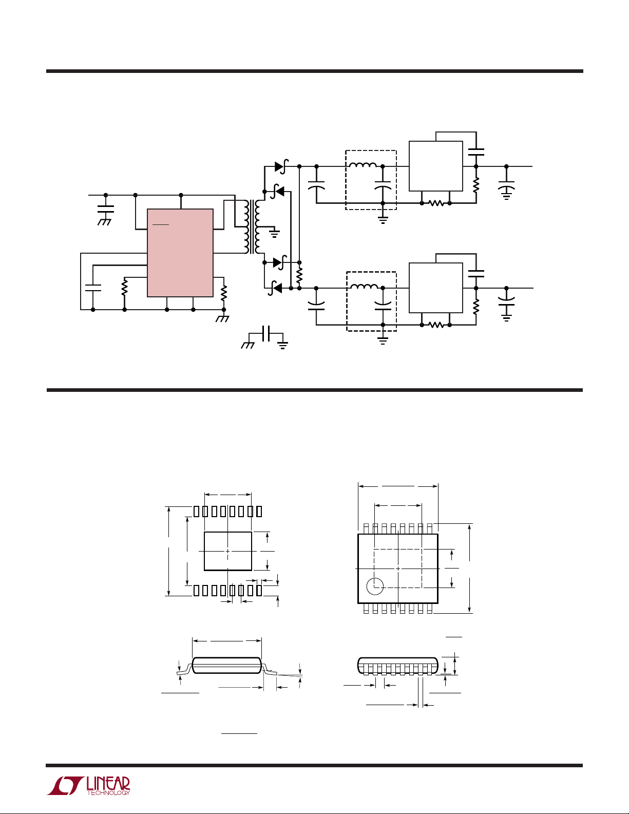
TYPICAL APPLICATIO
LT3439
U
Low Noise 5V to ±12V Push-Pull DC Transformer
V
IN
5V
C1: TAIYO YUDEN JMK212BJ475KG
C3-C6: SANYO OS-CON 20SVQP47M
C9, C10: SANYO OS-CON 16SVQPA39M
C11: AVX 1206AC222MA11A
D1-D4: MMBD914
L1, L2: COILCRAFT DT1608C-333
T1: COILTRONICS CTX02-16030
C
T
820pF
C1
4.7µF
R
T
16.9k
11
SHDN
5
SYNC
6
C
R
13
V
IN
LT3439
T
T
GND PGND
10
COLA
COLB
R
1, 16
SL
PACKAGE DESCRIPTIO
3
14
47
D1
+ + +
R8
10k
R
SI
16.9k
D2
T1
•
•
•
•
D3
D4
C11
2.2nF
1kV
U
FE Package
16-Lead Plastic TSSOP (4.4mm)
(Reference LTC DWG # 05-08-1663)
Exposed Pad Variation BA
2.74
(.108)
OPTIONAL
L1
C3
47µFC447µF
OPTIONAL
L2
C5
47µF
47µF
C6
+ +
4.90 – 5.10*
(.193 – .201)
2.74
(.108)
16 1514 13 12 11
BYP
LT1761-BYP
IN OUT
GND
ADJ
R2
49.9k
BYP
LT1964-BYP
IN OUT
GND
ADJ
R4
49.9k
10 9
C7
0.01µF
R1
442k
C8
0.01µF
R3
442k
3439 TA02
+
C9
39µF
C10
39µF
V
OUT
12V
80mA
V
OUT
–12V
80mA
6.60 ±0.10
4.50 ±0.10
RECOMMENDED SOLDER PAD LAYOUT
0.09 – 0.20
(.0036 – .0079)
NOTE:
1. CONTROLLING DIMENSION: MILLIMETERS
2. DIMENSIONS ARE IN
3. DRAWING NOT TO SCALE
Information furnished by Linear Technology Corporation is believed to be accurate and reliable.
However, no responsibility is assumed for its use. Linear Technology Corporation makes no representation that the interconnection of its circuits as described herein will not infringe on existing patent rights.
SEE NOTE 4
0.65 BSC
4.30 – 4.50*
(.169 – .177)
0.45 – 0.75
(.018 – .030)
MILLIMETERS
(INCHES)
2.74
(.108)
0.45 ±0.05
1.05 ±0.10
1345678
2
° – 8°
0
0.65
(.0256)
BSC
0.195 – 0.30
(.0077 – .0118)
4. RECOMMENDED MINIMUM PCB METAL SIZE
FOR EXPOSED PAD ATTACHMENT
*DIMENSIONS DO NOT INCLUDE MOLD FLASH. MOLD FLASH
SHALL NOT EXCEED 0.150mm (.006") PER SIDE
2.74
(.108)
1.10
(.0433)
MAX
0.05 – 0.15
(.002 – .006)
FE16 (BA) TSSOP 0203
6.40
BSC
sn3439 3439fs
11

LT3439
TYPICAL APPLICATIO
U
Low Noise 12V to –12V, 6W Push-Pull DC Transformer
V
12V
OPTIONAL
D1
•
•
C1: TDK C3216X5R1C475K
C3, C4: TDK C4532X5R1E156M
C5: TEK C3216X5R1C475K
D1, D2: MBRA130LT3
L1: COILCRAFT DO1608C-333
T1: COILTRONICS CTX02-16076
C3
15µF
D2
R
SI
16.9k
T1
•
•
IN
C1
4.7µF
C
T
680pF
C2
0.1µF
R
16.9k
11
SHDN
5
SYNC
6
C
R
T
13
V
IN
LT3439
T
T
GND PGND
10
COLA
COLB
R
1, 16
3
14
47
SL
L2
33µH
C4
15µF
IN
I
I
LIM2
LIM4
GND
LT1175
R1
150k
OUT
SENSE
R2
324k
C5
4.7µF
3439 TA03
V
OUT
–12V
500mA
RELATED PARTS
PART NUMBER DESCRIPTION COMMENTS
LT1533 Slew Rate Controlled Ultralow Noise 1A Switching Regulator VIN: 2.7V to 23V, IQ (Supply): 12mA, ISD: <12µA, SO-16, Low
Noise: <100µV
Current Slew Rates
LT1534/LT1534-1 Slew Rate Controlled Ultralow Noise 2A Switching Regulators VIN: 2.7V to 23V, IQ (Supply): 12mA, ISD: <12µA, SO-16, Low
Noise: <2mV
Current Slew Rates
LT1683 Slew Rate Controlled Ultralow Noise Push-Pull Controller VIN: 2.7V to 20V, IQ (Supply): 25mA, ISD: <24µA, SSOP-20, Low
Noise: <200µV
Current Slew Rates
LT1738 Slew Rate Controlled Ultralow Noise DC/DC Controller VIN: 2.7V to 20V, IQ (Supply): 12mA, ISD: <24µA, SSOP-20, Greatly
Reduced Conducted and Radiated EMI, Independent Control of
Switch Voltage and Current Slew Rates
LT1763 500mA, Low Noise Micropower, LDO VIN: 1.8V to 20V, V
0.30V, I
Q
: <1µA, SO-8, Low Noise: <20µV
I
SD
LT1764/LT1764A 3A, Low Noise, Fast Transient Response, LDOs VIN: 2.7V to 20V, V
0.34V, I
Q
DD, TO220-5, Low Noise: <40µV
Ceramic Capacitors
LT1962 300mA, Low Noise Micropower, LDO VIN: 1.8V to 20V, V
0.27V, I
Q
: <1µA, MS8, Low Noise: <20µV
I
SD
LT1963/LT1963A 1.5A, Low Noise, Fast Transient Response, LDOs VIN: 2.1V to 20V, V
0.34V, I
Q
DD, TO220-5, SOT-223, SO-8, Low Noise: <40µV
Stable with Ceramic Capacitors
LT1964 200mA, Low Noise Micropower, Negative LDO VIN: –0.9V to –20V, V
0.34V, I
Q
Low Noise: <30µV
ThinSOT is a trademark of Linear Technology Corporation.
Linear Technology Corporation
12
1630 McCarthy Blvd., Milpitas, CA 95035-7417
(408) 432-1900 ● FAX: (408) 434-0507
●
www.linear.com
, Independent Control of Switch Voltage and
P-P
, Independent Control of Switch Voltage and
P-P
, Independent Control of Switch Voltage and
P-P
: 1.22V, Dropout Voltage (V at I
(Supply): 30µA, V
(Supply): 1mA, V
(Supply): 30µA, V
(Supply): 1mA, V
(Supply): 30µA, V
OUT(MIN)
OUT(MIN)
OUT(MIN)
OUT(MIN)
OUT(MIN)
RMSP-P
: 1.5V, 1.8V, 2.5V, 3V, 3.3V, 5V,
OUT
RMSP-P
: 1.21V, Dropout Voltage (V at I
: 1.8V, 2.5V, 3.3V, ISD: <1µA,
OUT
, “A” Version Stable with
RMSP-P
: 1.22V, Dropout Voltage (V at I
: 1.5V, 1.8V, 2.5V, 3V, 3.3V, 5V,
OUT
RMSP-P
: 1.21V, Dropout Voltage (V at I
: 1.5V, 1.8V, 2.5V, 3.3V, ISD: <1µA,
OUT
: –1.21V, Dropout Voltage (V at I
: Adj, –5V, ISD: <3µA, ThinSOTTM,
OUT
, Stable with Ceramic Capacitors
LT/TP 0303 2K • PRINTED IN USA
LINEAR TECHNOLOGY CORP ORATION 2002
RMSP-P
):
OUT
):
OUT
):
OUT
):
OUT
, “A” Version
OUT
sn3439 3439fs
):
 Loading...