

Page 1
advertisement
Monolithic Step-Down Regulator Withstands The Rigors of
Automotive Environments and Consumes Only 100µA of
Quiescent Current – Design Note 378
Rich Philpott
Introduction
Automobile electronic systems place high demands on
today’s DC/DC converters. They must be able to precisely
regulate an output voltage in the face of wide temperature
and input voltage r anges—including load dump tr ansients
in excess of 60V and cold crank voltage drops to 4V. The
converter must also be able to minimize battery drain in
always-on systems by maintaining high effi ciency over a
broad load current range. Similar demands are made by
many 48V nonisolated t elecom applications, 40V FireWire
peripherals and battery-powered applications with auto
plug adaptors. The LT3437’s best in class performance
meets all of these requirements in a small thermally
enhanced 3mm × 3mm DFN package.
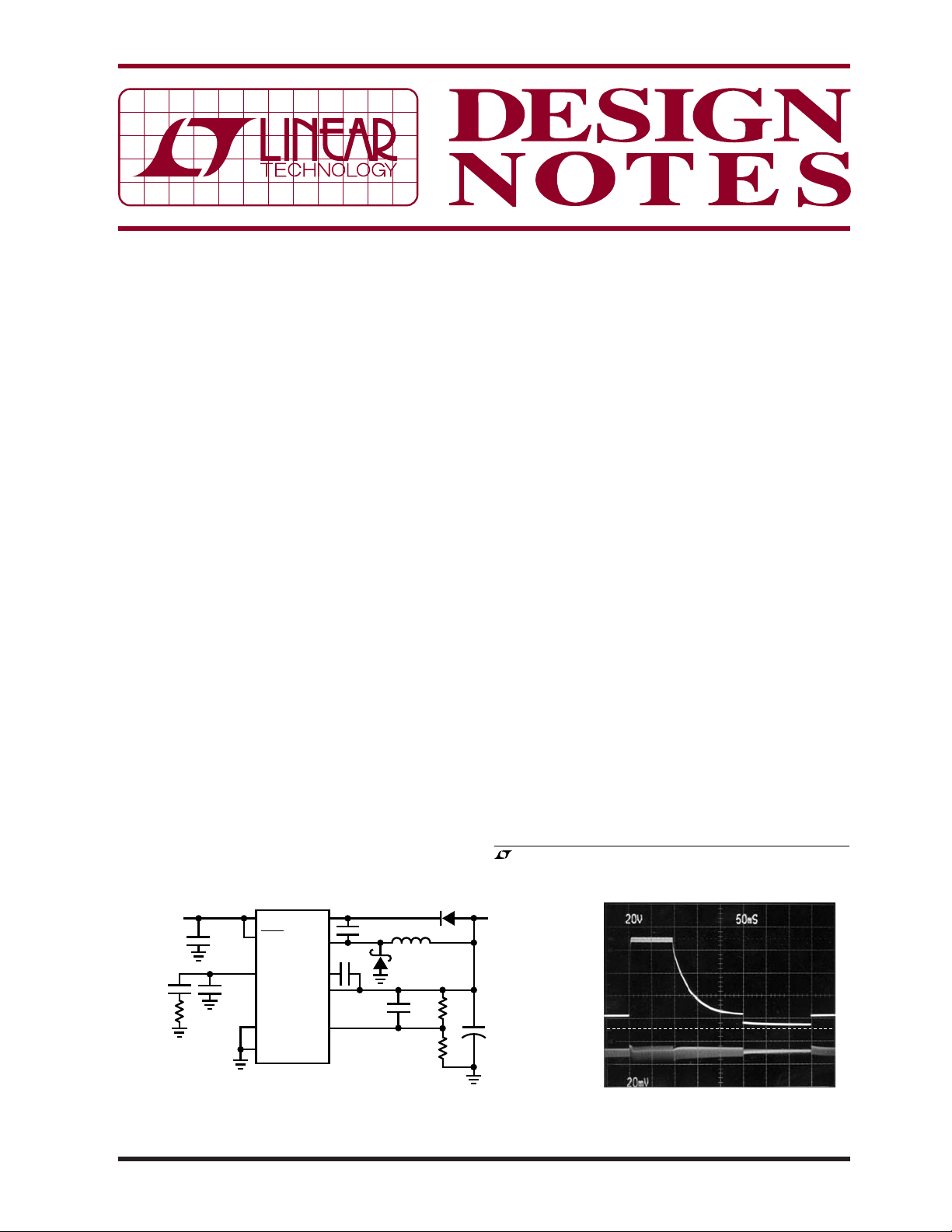
Features of the LT3437
The LT®3437 is a 200kHz fi xed frequency, 500mA
monolithic buck switching regulator. Its 3.3V to 80V
input voltage range makes the LT3437 ideal for harsh
automotive environments. Micropower bias current and
®
Burst Mode
operation help to maintain high effi ciency
over the entire load range and result in a no load quiescent current of only 100µA for the circuit in Figure 1. The
LT3437 has an undervoltage lockout and a shutdown pin
with an accurate threshold for a <1µA quiescent current
shutdown mode.
V
3.75V TO 80V*
IN
2.2µF
100V
CER
1500pF
24k
*FOR INPUT VOLTAGES ABOVE 60V SOME RESTRICTIONS MAY APPLY.
SEE ABSOLUTE MAXIMUM RATINGS IN DATA SHEET
330pF
V
IN
SHDN
V
C
SYNC
GND
LT3437
BOOST
SW
C
V
BIAS
100µH
0.1µF
0.1µF
SS
27pF
FB
10MQ100N
BAS21
165k
100k
+
External synchronization can be implemented by driving
the SYNC pin with a logic-level input. The SYNC pin also
doubles as Burst Mode defeat for applications where
lower output ripple is desired over light load effi ciency. A
single capacitor prov ides soft-star t capability w hich limits
inrush current and output vol tage overshoot during star tup
and recovery from brown-out situations. The LT3437 is
available in either a low profi le 3mm × 3mm 10-pin DFN
or 16-pin TSSOP package both with an exposed pad
leadframe for low thermal resistance.
Brutal Input Transients
Figure 2 shows the LT3437’s reaction to the severe input
transients that are possible in an automotive environment. Here, the input voltage rises from a nominal 12V
to 80V in a 100ms load dump pulse, then drops to 4V in
a 150ms cold crank pulse. The 200kHz fi xed frequency
and current mode topology of the LT3437 allow it to take
it all in its stride—response to the input transients are
less than 1% of the regulated voltage.
The fuzziness seen on the output voltage is due to the
ESR of the output capacitor and the change in inductor
current ripple as the input voltage transitions between
, LTC, LT and Burst Mode are registered trademarks of Linear Technology
Corporation. All other trademarks are the property of their respective owners.
V
OUT
3.3V
250mA
100µF
6.3V
TANT
DN378 F01
V
20V/DIV
V
OUT
20mV/DIV
AC COUPLED
IN
0V
LOAD DUMP
COLD CRANK
50ms/DIV
DN378 F02
12/05/378
Figure 1. 14V to 3.3V Step-Down Converter
with 100µA No Load Quiescent Current
Figure 2. Output Voltage Response to Load
Dump and Cold Crank Input Transients
Page 2
levels. This ripple can be eliminated by changing the
output capacitor type from tantalum to ceramic.
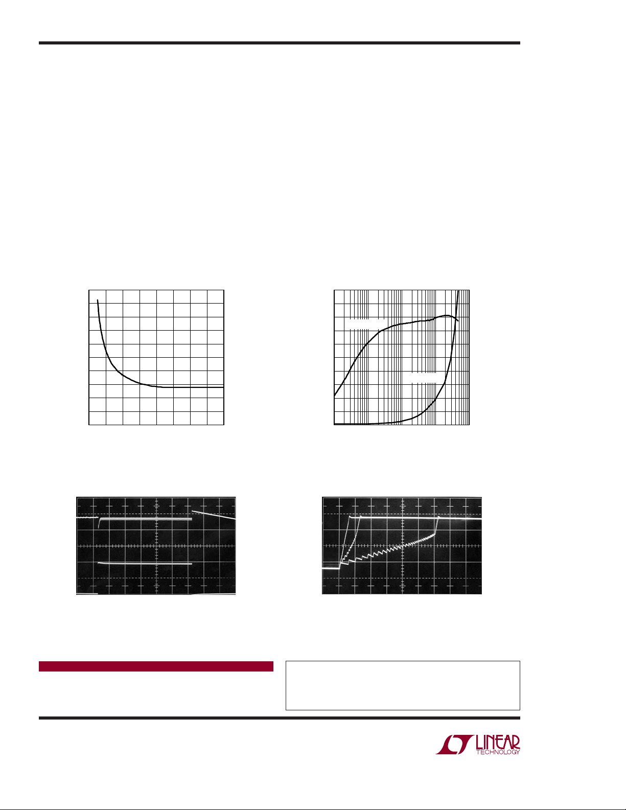
Low Quiescent Currents
Many of today’s automotive applications are migrating to
always-on systems which require low average quiescent
current to prolong battery life. Loads are switched off
or reduced during low demand periods, then activated
for short periods. Quiescent current for the application
circuit in Figure 1 is less than 1µA in shutdown mode,
and a mere 100µA (Figure 3) for an input voltage of 12V
under a no load condition. The LT3437 provides excellent
step response from a no-load to load situation as shown
in Figure 4. Automatic Burst Mode
operation ensures
effi ciency over the entire load range as seen in Figure 5.
Burst Mode
operation can be defeated if lower ripple is
desired over light load effi ciency by pulling the SYNC pin
high or driving it with an ex ternal clock.
200
180
160
140
120
100
80
60
SUPPLY CURRENT (µA)
40
20
0
0
10 20 30 40 50 60 70
INPUT VOLTAGE (V)
80
DN378 F03
Soft-Start Capability
The rising slope of the output voltage is determined by
the output voltage and a single capacitor. Initially, when
the output voltage is close to zero, the slope of the output
is determined by the soft-start capacitor. As the output
voltage increases, the output slope is increased to full
bandwidth near the regulated voltage. Since the circuit
is always active, inrush current and voltage overshoot
are minimized for startup and recovery from overload
(brown-out) conditions. Figure 6 illustrates the effect of
several soft-start capacitor values.
Conclusion
The LT3437’s wide input range, low quiescent current,
robust design and small thermally enhanced packages
make it an ideal solution for all automotive and wide input
voltage, low quiescent current applications.
100
90
80
70
60
50
40
EFFICIENCY (%)
30
20
10
0
EFFICIENCY
POWER LOSS
1 10 100
LOAD CURRENT (mA)
DN378 F05
500
450
400
350
300
250
200
150
100
50
0
1k0.1
POWER LOSS (mW)
Figure 3. Supply Current vs Input Voltage
for Circuit in Figure 1
V
OUT
50mV/DIV
200mA
I
OUT
100mA/DIV
0mA
1ms/DIV
DN378 F04
Figure 4. Output Voltage Response for
0mA to 200mA Load Step
Data Sheet Download
http://www.linear.com
Linear Technology Corporation
1630 McCarthy Blvd., Milpitas, CA 95035-7417
(408) 432-1900
●
FAX: (408) 434-0507 ● www.linear.com
Figure 5. Effi ciency and Power Loss vs
Load Current for the Circuit in Figure 1
CSS = GND
C
V
OUT
1V/DIV
OUT
I
LOAD
V
IN
= 100µF
= 200mA
= 12V
C
SS
= 0.01µF
1ms/DIVC
= 0.1µF
SS
DN378 F06
Figure 6. Output Voltage Soft-Start
For applications help,
call (408) 432-1900, Ext. 2759
dn378f LT/TP 1205 409K • PRINTED IN THE USA
© LINEAR TECHNOLOGY CORPORATION 2005
 Loading...