

advertisement
60V, 3A Step-Down DC/DC Converter Has Low Dropout and
100µA Quiescent Current
– Design Note 352
Keith Szolusha
Introduction
High voltage bipolar monolithic step-down converters are
usually optimized for high efficiency at
rents, often at the expense of light load efficiency and
operation near dropout. The problem is that a 2mA
quiescent current at zero load drains batteries in applications that spend long periods of time at minimum load
current. One common solution for reducing quiescent
current and improving battery run-time is a shutdown
function, but shutdown drops the output voltage to zero.
Shutdown is not acceptable in systems where a constant
regulated output voltage is required for light load applications, system diagnostics and ready-to-use load transients. In some systems, a regulated output voltage is
needed at very low input voltage (low dropout). Simply
shutting down the converter to zero output to avoid output
droop is not always an option.
®
The LT
3434, 3A monolithic buck switching regulator is
designed to optimize efficiency over
age levels, both high and low. Micropower bias current
and Burst Mode® operation enable it to consume merely
100µA at zero load and 12V input. The high efficiency
bipolar NPN power switch (0.1Ω) provides up to 85%
efficiency at a 2A load current. Combined with high duty
high
output cur-
all
current and volt-
cycle, the low dropout of the switch maintains a regulated
3.3V output down to 4V input at all load currents. This is
important for automotive cold-crank operation.
The LT3434’s 3.3V to 60V input voltage range makes it
ideal for 14V and 42V automotive battery-fed applications
with both 4V cold crank and high input voltage transients
(up to 60V). The 3A switch current rating provides maximum load currents of up to 2.5A. The LT3434 maintains
output regulation down to 4V input for 3.3V output and
down to 3.3V input for 2.5V or lower output voltages.
The high input voltage and low quiescent current make
this an ideal choice for many 48V nonisolated telecom
applications, 40V FireWire
®
peripherals and multisource
battery-powered applications with autoplug adaptors.
The LT3434 can survive load-dump input transients up to
60V that are common in these systems.
It also includes other important features to shrink solution size, simplify configuration and improve system
robustness:
• Fixed 200kHz switching frequency provides low output
ripple, high efficiency and the ability to provide wide
, LTC, LT and Burst Mode are registered trademarks of Linear Technology
Corporation. FireWire is a registered trademark of Apple Computer, Inc.
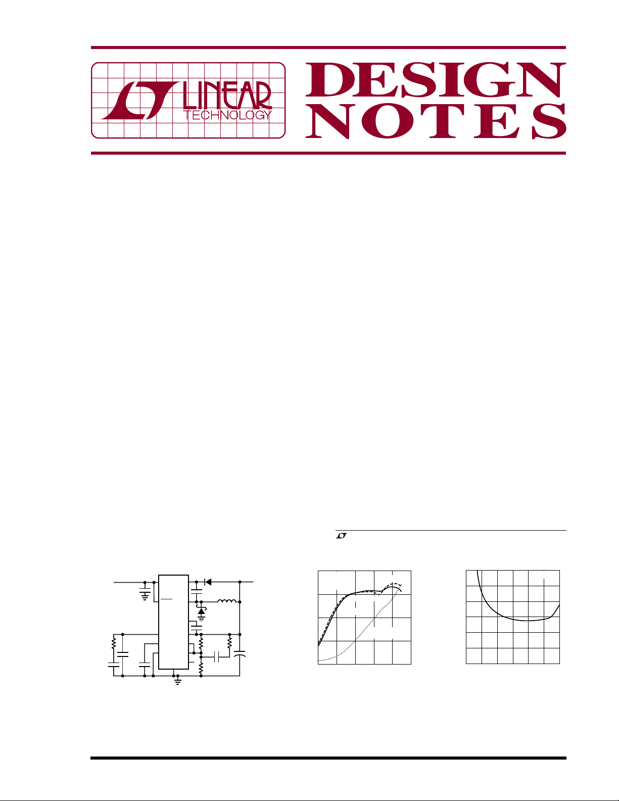
DIODES INC.
V
IN
4V TO 60V
4.7µF 100V
TDK C5750X7R2A475M
CERAMIC
R1
4.7k
470pF
0.01µF
0.01µF
V
IN
SHDN
V
C
C
T
SYNC
LT3434
GND
BOOST
V
BIAS
PGFB
1N4448W
33µH
COOPER
0.68µF
DIODES INC.
B360
0.01µF
165k
1%
10pF
100k
1%
UP3B-330
24k
SW
C
SS
FB
PG
+
DN352 F01
V
OUT
3.3V
2A
100µF
6.3V ×2
KEMET
A700D107M006ATE
ALUMINUM
ORGANIC
Figure 1. LT3434 Wide Input Voltage Range
DC/DC Converter Application to 3.3V Output at
2A Load Current Featuring Burst Mode
Operation for Light Load Operation and 4V Low
Dropout Operation
11/04/352
100
VIN = 12V
L = 33µH
C
OUT
75
50
EFFICIENCY (%)
25
0
0.0001
= 100µF
V
OUT
0.001
LOAD CURRENT (A)
EFFICIENCY
= 3.3V
0.01
V
TYPICAL POWER
LOSS
0.1 1
10
= 5V
OUT
1
POWER LOSS (W)
0.1
0.01
0.001
10
DN352 F02
Figure 2. The Efficiency of Figure 1
is Typically Greater Than 75%. At
Light Loads, Suppy Current is
Minimized with Burst Mode
Operation
150
125
100
75
50
SUPPLY CURRENT (µA)
25
0
0
10
20
INPUT VOLTAGE (V)
30 40
V
= 3.3V
OUT
50
60
DN352 F03
Figure 3. With Zero Load
Current, the Supply Current to
the LT3434 is Extremely Low,
Typically Below 100µA (VIN ≥
12V)
input voltage range solutions. The LT3434 can be
synchronized at frequencies up to 700kHz.
• The shutdown pin provides a 2.38V undervoltage lockout threshold as well as a 0.4V threshold for micropower
shutdown (<1µA).
• A single capacitor provides soft-start capabilities and
limits inrush current and output voltage overshoot in
sensitive applications.
A power good flag and power good comparator provide
•
the system with an indication that the output voltage,
the input voltage or some other line is above a desired
voltage.
• The LT3434 is provided in a small 16-pin TSSOP thermally enhanced package for excellent thermal
performance.
Burst Mode Operation
Figure 1 shows a typical wide input voltage range step-down
application to 3.3V output DC/DC converter. Burst Mode
operation reduces light load quiescent current by disabling
switching for a number of switch cycles and placing the part
briefly in micropower shutdown until switching begins
again. Bursts of switch pulses are enough to maintain
output voltage regulation at light load. Figure 2 shows that
the efficiency is high for nominal loads, between 100mA
and 2A, and that at light load the quiescent current only sips
from the battery during long periods of system inactivity.
Figure 3 shows that for most typical input voltages, zero
load quiescent current is below 100µA.
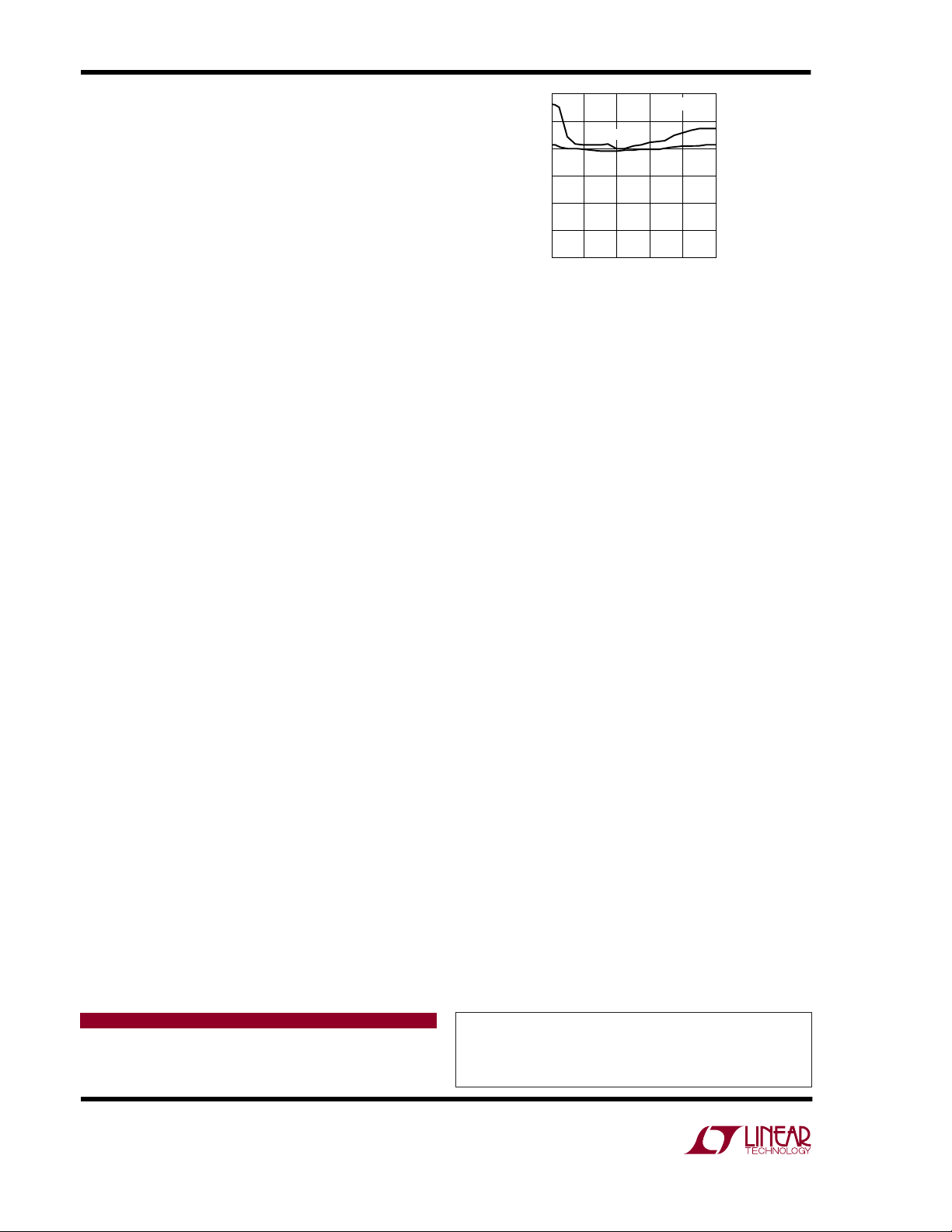
Low Dropout
The LT3434 provides extremely low dropout with high
maximum duty cycle (90%) and low power switch
on-resistance (0.1Ω). Figure 4 demonstrates how the
LT3434 maintains 3.3V output regulation with an input
voltage down to 4V over the entire load current range. The
minimum input voltage required to start up the output is
slightly higher, as shown in Figure 4. Starting up the LT3434
at a duty cycle lower than maximum helps get the boost
voltage high enough to run the power switch in low V
CE(SAT)
operation before entering extremely low dropout.
Soft-Start
Only a single capacitor (CSS in Figure 1) is required for
soft-start. Soft-start avoids the problems created by
large inrush currents at start-up, where switchers without
(V)
V
6
5
4
3
IN
2
1
0
0
START-UP
RUN
0.4 0.8 1.2 1.6
LOAD CURRENT (A)
V
= 3.3V
OUT
2
DN352 F04
Figure 4. Low Dropout Operation for 3.3V Output is as
Low as 4V Over the Entire Load Current Range. Start-Up
Requires Slightly Higher Input Voltage
soft-start try to go from zero to regulation by consuming
as much current as possible from the source and casting
it into the output capacitor and load. This surge of current
can both drag down a battery source voltage and cause
overshoot in the output voltage. The soft-start capacitor
for the LT3434 holds the peak current level clamp low,
allowing it to slowly rise upon start-up. An external softstart capacitor removes the inrush current surge and
limits output voltage overshoot by controlling the output
voltage ramp-up rate.
Power Good
For systems that rely upon having a well regulated power
source or that follow a particular power-up sequence, the
LT3434 provides a power good flag with programmable
delay. The delay is programmed by C
power good feedback pin exceeds 90% of V
, starting when the
T
(1.25V).
REF
By tying the power good feedback pin (PGFB) directly to
the feedback pin (FB), the power good comparator returns
a “good” signal only when the output voltage has reached
90% and the C
voltage exceeds its internal clamp. The
T
power good feedback pin can also be tied to the input
voltage, an external source or a resistor divider on any of
these sources.
Conclusion
The LT3434 is a wide input voltage range, 200kHz, monolithic 3A, step-down DC/DC converter. High input voltage,
high power switch capabilities, low quiescent current, low
dropout and excellent package thermal conductivity make
this an extremely useful and versatile IC that is simple to
use in many step-down applications.
Data Sheet Download
http://www.linear.com
Linear Technology Corporation
1630 McCarthy Blvd., Milpitas, CA 95035-7417
(408) 432-1900 ● FAX: (408) 434-0507 ● www.linear.com
For applications help,
call (408) 432-1900, Ext. 2759
dn352f LT/TP 1104 409K • PRINTED IN THE USA
© LINEAR TECHNOLOGY CORPORATION 2004
 Loading...