

advertisement
High Input Voltage Monolithic Switcher Steps Up and Down
Using a Single Inductor – Design Note 330A
Jay Celani
Introduction
Ultrawide input voltage requirements are a common
design problem for DC/DC converter applications, but
when that range includes voltages both above and below
the output voltage, the converter must perform both
step-up and step-down functions. The LT
®
3433 is a high
voltage monolithic DC/DC converter that incorporates
two switch elements, allowing for a unique topology that
accommodates both step-up and step-down conversion
using a single inductor.
The LT3433 uses a 200kHz constant frequency, current
mode architecture and operates with input voltages from
4V to 60V. An internal 1% accurate voltage reference
allows programming of precision output voltages up to 20V
using an external resistor divider. Burst Mode
®
operation
improves efficiencies during light-load conditions, reducing the device’s quiescent current to 100µA during no-load
conditions. A soft-start feature reduces output overshoot
and inrush currents during start-up, and both current limit
foldback and frequency foldback are employed to control
inductor current runaway during start-up and short-circuit
conditions. The LT3433 is available in a 16-pin fused TSSOP
exposed pad package which provides a small footprint and
excellent thermal characteristics.
When the converter input voltage is significantly higher
than the output voltage, the LT3433 operates as a modified buck converter using a boosted-drive high side switch.
If the converter input voltage becomes close enough to
the output voltage to require a duty cycle greater than 75%
in buck mode, the LT3433 automatically enables a second
switch. This second switch pulls the output side of the
switched inductor to ground during the “switch on” time,
creating a bridged switching configuration.
During bridged switching, the LT3433 merges the elements
of buck and boost DC/DC converters as shown in Figure␣ 1.
In the simplest terms, a buck DC/DC converter switches
the V
switches the V
side of the inductor, while a boost converter
IN
side of the inductor. Combining the
OUT
elements of both topologies achieves both step-up and
step-down functionality using a single inductor, so voltage conversion can continue when VIN approaches or is
less than V
OUT
.
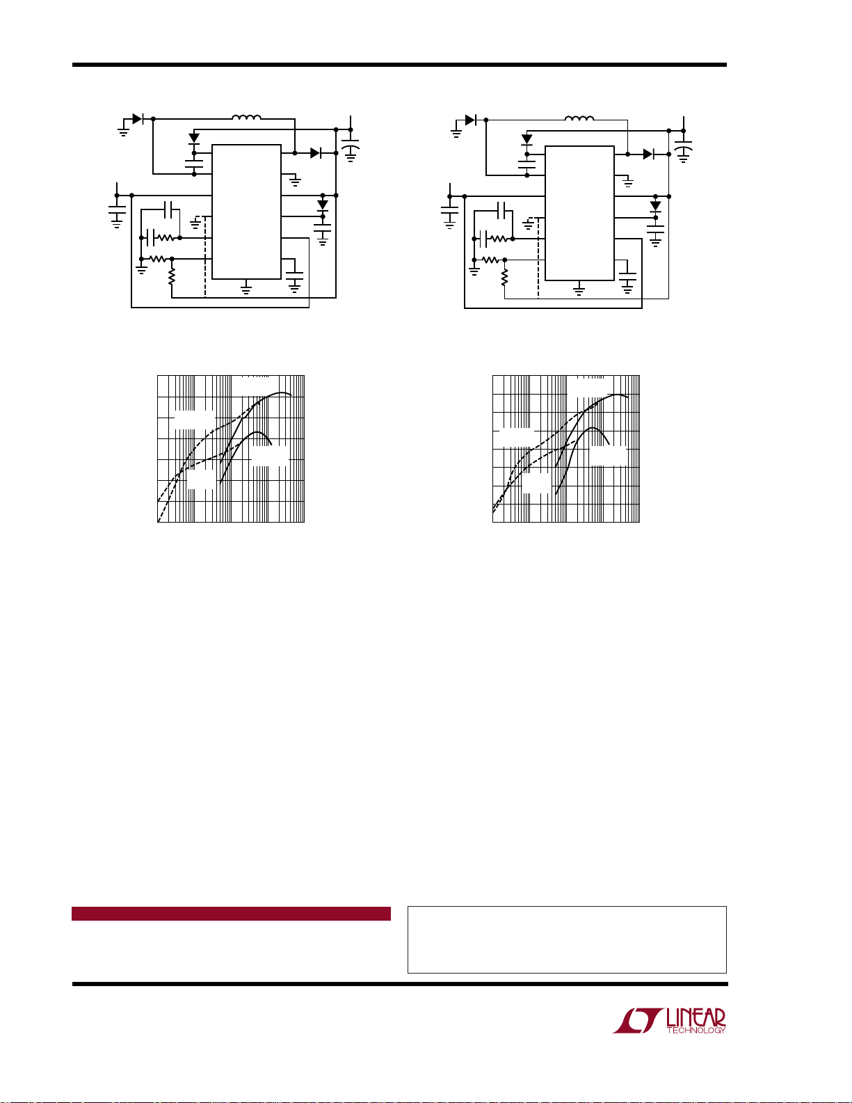
4V-60V Input to 5V Output
DC/DC Automotive Converter
A 4V-60V to 5V DC/DC converter is shown in Figure 2. This
converter is well suited for 12V automotive battery applications, maintaining output voltage regulation with battery line voltages from 4V cold crank through 60V load
dump. The threshold for bridged mode operation is about
8V, so the converter will operate primarily in buck mode
except during a cold crank condition. During buck operation, this converter can provide load currents up to 350mA
with input voltages up to 60V. Operating with a nominal
13.8V input, this LT3433 converter accommodates loads
of 400mA and produces efficiencies up to 82%.
When the input voltage drops below 8V, the converter
switches into bridged operation to maintain output voltage regulation. Because the LT3433 switch current limit is
, LTC, LT and Burst Mode are registered trademarks of Linear Technology
Corporation.
SW
V
IN
C
(1a) Step-Down (VIN > V
V
IN
C
(1b) Step-Up (VIN < V
SW
V
IN
C
(1c) Step-Up/Step-Down (VIN > V
Figure 1. The LT3433 Merges the Elements of
Step-Up and Step-Down DC/DC Converters
L
D
IN
L
IN
L
DSW
IN
D
SW
OUT
D
OUT
V
OUT
C
OUT
)
OUT
V
OUT
C
OUT
)
V
OUT
C
OUT
DN330A F01
or VIN < V
OUT
)
02/04/330A
B160A
100µH
CoEv DU1352-101M
4V ≤ V
8.5V ≤ V
V
OUT
5V
≤ 8.5V: 125mA
IN
≤ 60V: 350mA
IN
B160A
220µH
TDK SLF12565T-221M1R0
8V ≤ V
18V ≤ V
V
OUT
12V
≤ 18V: 125mA
IN
≤ 60V: 380mA
IN
2.2µF
100V
CERAMIC
1N4148
V
IN
4V TO 60V
330pF
1nF
100k
305k
68k
0.1µF
10V
(BURST)
(NO
BURST)
V
SW_H
V
BURST_EN
V
V
SW_L
BST
PWRGND
LT3433
V
IN
C
FB
SGND
OUT
V
BIAS
SHDN
1N4148
0.1µF
SS
Figure 2. 4V-60V to 5V DC/DC Converter
90
80
VIN = 13.8V
70
60
50
EFFICIENCY (%)
40
30
20
BURST
VIN = 4V
BURST
0.1 10 100 1000
1
OUTPUT CURRENT (mA)
VIN = 13.8V
NO BURST
VIN = 4V
NO BURST
DN330A F03
10V
B120A
0.01µF
DN330A F02
+
47µF
10V
MODE SWITCH
H-L: 7.9V
V
IN
L-H: 8.3V
V
IN
2.2µF
100V
CERAMIC
1N4148
V
(BURST)
(NO
BST
SW_H
LT3433
V
IN
BURST_EN
V
C
V
FB
SGND
V
IN
8V TO 60V
330pF
1nF
20k
176k
0.47µF
50V
68k
BURST)
Figure 4. 8V-60V to 12V Converter
100
90
80
70
VIN = 20V
BURST
60
50
EFFICIENCY (%)
40
30
20
VIN = 8V
BURST
0.1 10 100 1000
1
OUTPUT CURRENT (mA)
VIN = 20V
NO BURST
SW_L
PWRGND
V
OUT
V
BIAS
SHDN
VIN = 8V
NO BURST
+
B120A
1N4148
0.1µF
10V
SS
0.01µF
DN330A F04
DN330A F05
47µF
25V
MODE SWITCH
H-L: 16.6V
V
IN
L-H: 17V
V
IN
Figure 3. 4V-60V to 5V Conversion Efficiency
fixed, converter load capability is reduced while operating
in bridged mode. With an input of 4V, the converter
accommodates loads up to 125mA. Not only does this
LT3433 converter operate across a large range of DC input
voltages, but it also maintains tight output regulation
during input transients. When subjected to a 1ms 13.8V
to 4V input transition to simulate a cold crank condition,
regulation is maintained to 1% with a 125mA load.
8V-60V Input to 12V Output DC/DC Converter
As converter output voltages increase, switch current
and duty-cycle limitations prevent operation with V
at
IN
the extreme low end of the LT3433 operational range.
The 12V output converter shown in Figure 4 can provide
load current up to 125mA with an input voltage as low as
8V. This is suitable for 12V automotive applications
without cold-crank requirements, as well as many other
Data Sheet Download
http://www.linear.com/go/dnLT3433
Figure 5. 8V-60V to 12V Conversion Efficiency
applications such as those powered by inexpensive wall
adapters. This converter operates in buck mode with
input voltages above 17V, accommodating loads up to
380mA. This converter accommodates loads up to 435mA
and produces efficiencies above 89% at 20V input.
Conclusion
The LT3433 simplifies ultrawide input range DC/DC voltage conversion, enabling simple and inexpensive solutions
to a variety of design problems. Automatic transitioning
between buck and bridged modes of operation provides
seamless output regulation for wide input voltage ranges
and input voltage transients. The use of a small footprint
TSSOP package, a single inductor and few external components reduce board space requirements, increase efficiency and improve thermal characteristics.
For applications help,
call (408) 432-1900, Ext. 2759
Linear Technology Corporation
1630 McCarthy Blvd., Milpitas, CA 95035-7417
(408) 432-1900 ● FAX: (408) 434-0507 ● www.linear.com
dn330Af LT/TP 0204 344K • PRINTED IN THE USA
LINEAR TECHNOLOGY CORPORATION 2004
 Loading...