

查询LT3420EDD供应商
Chargers with Automatic Refresh
FEATURES
■
Charges 220µF to 320V in 3.7 Seconds
from 5V (LT3420)
■
Charges 100µF to 320V in 3.5 Seconds
from 5V (LT3420-1)
■
Charges Any Size Photoflash Capacitor
■
Supports Operation from Two AA Cells or Any
Supply from 1.8V to 16V
■
Controlled Peak Switch Current: 1.4A (LT3420)
1.0A (LT3420-1)
■
Controlled Input Current: 840mA (LT3420)
450mA (LT3420-1)
■
Uses Standard Transformers
■
Efficient Flyback Operation (>75% Typical)
■
Adjustable Output
■
Automatic Refresh
■
Charge Complete Indicator
■
No High Voltage Zener Diode Required
■
No Output Voltage Divider Required
■
Small 10-Lead MSOP Package
■
Small 10-Lead (3mm × 3mm) DFN Package
U
APPLICATIO S
■
Digital Camera Flash Unit
■
Film Camera Flash Unit
■
High Voltage Power Supplies
LT3420/LT3420-1
Photoflash Capacitor
U
DESCRIPTIO
The LT®3420/LT3420-1 charge high voltage photoflash
capacitors quickly and efficiently. Designed for use in both
digital and film cameras, these devices use a flyback
topology to achieve efficiencies up to four times better
than competing flash modules. A unique adaptive off-time
control algorithm* maintains current-limited continuous
mode transformer operation throughout the entire charge
cycle, eliminating the high inrush current often found in
modules.
The LT3420/LT3420-1 output voltage sensing scheme*
monitors the flyback voltage to indirectly regulate the
output voltage, eliminating an output resistor divider or
discrete zener diode. This feature allows the capacitor to
be held at a fully charged state without excessive power
consumption. Automatic refresh (which can be defeated)
allows the capacitor to remain charged while consuming
an average input current of about 2mA, at a user-defined
refresh rate. A logic high on the CHARGE pin initiates
charging, while the DONE pin signals that the capacitor is
fully charged.
The LT3420/LT3420-1 are available in 10-Lead MSOP and
(3mm × 3mm) DFN packages.
, LTC and LT are registered trademarks of Linear Technology Corporation. All other
trademarks are the property of their respective owners. *Protected by U.S. Patents
including 6518733.
U
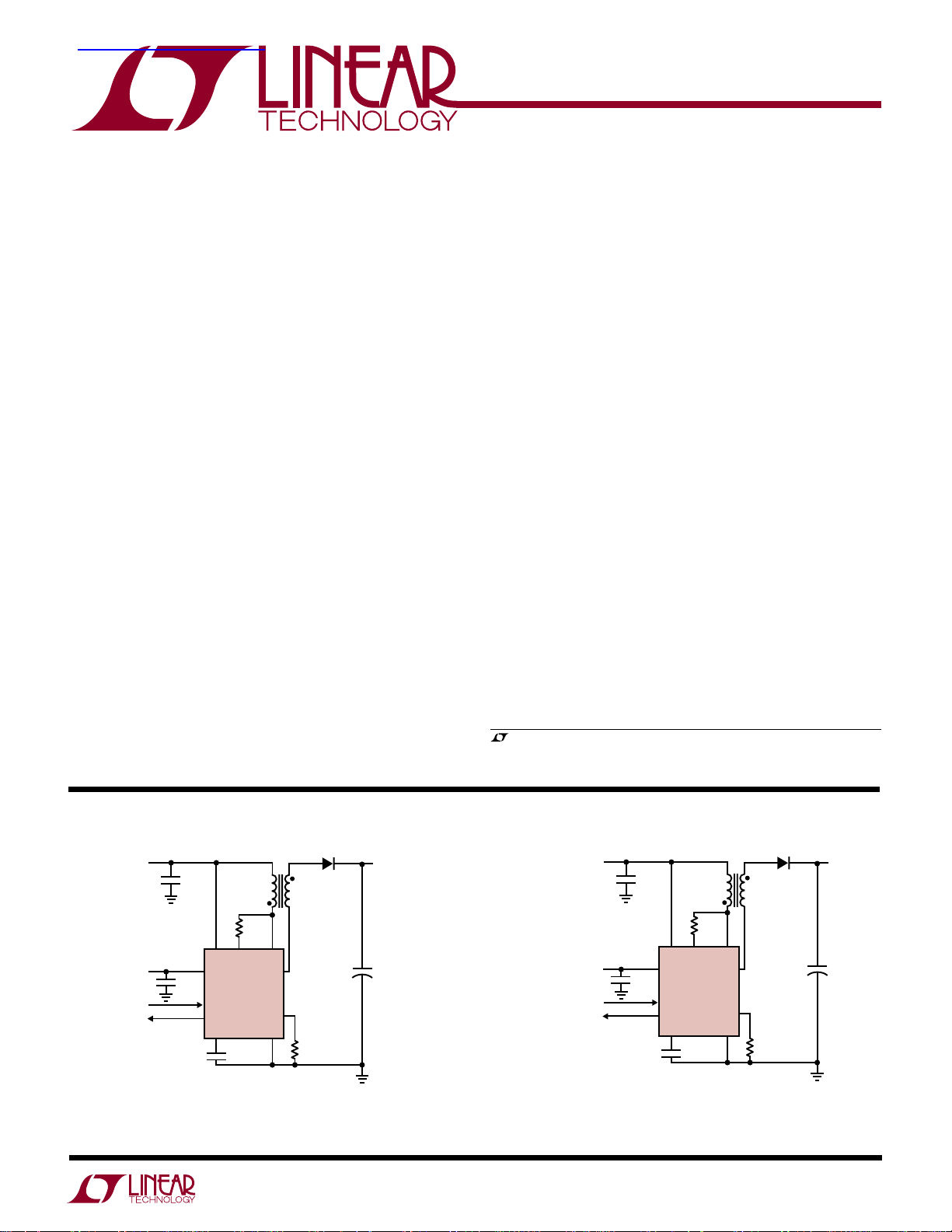
TYPICAL APPLICATIO
T1
LT3420
0.1µF
51.1k
1:12
8
5,6
3,4
632
SW
SEC
R
REF
GND
1
7
PHOTOFLASH
1
2k
D1
220µF
330V
CAPACITOR
C3
+
V
BAT
1.8V TO 6V
INPUT CURRENT
≈350mA
V
2.5V TO 10V
CHARGE
DONE
C1, C2: 4.7µF, X5R or X7R, 10V
C3: RUBYCON 220µF PHOTOFLASH CAPACITOR
T1: TDK SRW10EPC-U01H003 FLYBACK TRANSFORMER
D1: VISHAY GSD2004S SOT-23
DUAL DIODE. DIODES CONNECTED IN SERIES
C1
4.7µF
V
BATRFB
C2
4.7µF
4
V
9
CHARGE
8
DONE
C
CC
T
10 5
CC
Figure 1. High Charge Rate LT3420 Photoflash Circuit
320V
DANGER HIGH VOLTAGE
OPERATION BY HIGH VOLTAGE
3420 F01
TRAINED PERSONNEL ONLY
T1
60.4k
LT3420-1
0.1µF
1:10
(3mm TALL)
4
3
632
SW
SEC
1
R
REF
GND
5
6
7
PHOTOFLASH
CAPACITOR
2k
D1
100µF
330V
320V
C3
+
3420 F02
V
BAT
1.8V TO 6V
INPUT CURRENT
≈450mA
V
2.5V TO 6V
CHARGE
DONE
C1, C2: 4.7µF, X5R or X7R, 6.3V
C3: RUBYCON 100µF PHOTOFLASH CAPACITOR
T1: KIJIMA MUSEN SBL-5.6S-2
D1: VISHAY GSD2004S SOT-23
DUAL DIODE. DIODES CONNECTED IN SERIES
C1
4.7µF
V
BATRFB
C2
4.7µF
4
V
9
CHARGE
8
DONE
C
CC
T
10 5
CC
Figure 2. Small Size LT3420-1 Photoflash Circuit
3420fb
1

LT3420/LT3420-1
WW
W
U
ABSOLUTE AXI U RATI GS
(Note 1)
V
Voltage .............................................................. 16V
CC
Voltage ............................................................ 16V
V
BAT
SW Voltage (Note 2)
LT3420 ................................................................ 38V
LT3420-1............................................................ 50V
SEC Current ...................................................... ±200mA
RFB Current ........................................................... ±3mA
R
Voltage ........................................................... 2.5V
REF
CHARGE Voltage...................................................... 16V
CT Voltage .............................................................. 1.5V
U
W
PACKAGE/ORDER INFORMATION
TOP VIEW
R
1
REF
V
2
BAT
3
R
FB
4
V
CC
5
GND
10-LEAD (3mm × 3mm) PLASTIC DFN
T
JMAX
DD PACKAGE
= 125°C, θJA = 43°C/W, θJC = 3°C/W
EXPOSED PAD IS GND (PIN 11)
AND MUST BE SOLDERED TO PCB
10
C
CHARGE
9
11
DONE
8
7
SEC
6
SW
T
ORDER PART
NUMBER
LT3420EDD
LT3420EDD-1
DD PART
MARKING
LBJW
LBJX
DONE Voltage .......................................................... 16V
Current into DONE Pin .......................................... ±1mA
Maximum Junction Temperature .......................... 125°C
Operating Ambient Temperature Range
(Note 3) .............................................. –40°C to 85°C
Storage Temperature Range ................. –40°C to 125°C
Lead Temperature (Soldering, 10 sec)
(For MS Package only) ..................................... 300°C
U
ORDER PART
TOP VIEW
1
R
REF
V
2
BAT
R
3
FB
V
4
CC
GND
5
MS PACKAGE
10-LEAD PLASTIC MSOP
T
= 125°C, θJA = 100°C/W, θJC = 45°C/W
JMAX
(4-LAYER BOARD)
10
9
8
7
6
C
T
CHARGE
DONE
SEC
SW
NUMBER
LT3420EMS
LT3420EMS-1
MS PART MARKING
LTYH
LTAJG
Consult LTC Marketing for parts specified with wider operating temperature ranges.
ELECTRICAL CHARACTERISTICS
temperature range, otherwise specifications are at TA = 25°C. VCC = V
PARAMETER CONDITIONS MIN TYP MAX UNITS
Minimum Operating Voltage, V
Maximum Operating Voltage, V
VCC UVLO Hysteresis 40 mV
Minimum V
Maximum V
V
UVLO Hysteresis 275 mV
BAT
R
Threshold Voltage 0.98 1.00 1.02 V
REF
R
Pin Bias Current V
REF
Quiescent Current V
Quiescent Current in Shutdown V
Voltage 1.6 1.8 V
BAT
Voltage 16 V
BAT
CC
CC
The ● denotes the specifications which apply over the full operating
= 3.3V, V
BAT
= 0V, Switching 2 4 µA
RREF
V
= V
RFB
RREF
CHARGE
– 0.2V (Note 4)
BAT
= 1.1V, Not Switching 90 130 µA
= 0V, VIN = 3.3V 0.01 1 µA
= VCC unless otherwise noted. (Note 3)
CHARGE
● 2.2 2.5 V
● 0.975 1.025 V
16 V
3420fb
2
LT3420/LT3420-1
ELECTRICAL CHARACTERISTICS
temperature range, otherwise specifications are at T
The ● denotes the specifications which apply over the full operating
= 25°C. VCC = V
A
= 3.3V, V
BAT
= VCC unless otherwise noted. (Note 3)
CHARGE
PARAMETER CONDITIONS MIN TYP MAX UNITS
Primary Side Current Limit LT3420 (Note 5) 1.20 1.4 1.60 A
LT3420-1 (Note 5) 0.75 0.9 1.05 A
Secondary Side Current Limit LT3420 (Note 5) 20 40 50 mA
LT3420-1 (Note 5) 5 15 25 mA
Leakage Blanking Pulse Width LT3420 200 ns
LT3420-1 0 ns
Refresh Timer Charge/Discharge Current VCT = 0.75V 1.5 2.5 3.5 µA
Refresh Timer Upper Threshold 0.9 1.0 1.1 V
Refresh Timer Lower Threshold 0.45 0.5 0.55 V
Switch V
CESAT
LT3420, SW = 1A (Note 5) 220 340 mV
LT3420-1, SW = 0.5A (Note 5) 130 230 mV
Switch Leakage Current VSW = 38V (LT3420), VSW = 50V (LT3420-1) 0.01 1 µA
CHARGE Input Voltage High 1.5 V
CHARGE Input Voltage Low 0.2 V
CHARGE Pin Bias Current V
V
= 3V 4.5 15 µA
CHARGE
= 0V 0.01 0.1 µA
CHARGE
DONE Output Signal High 100k from VCC to DONE 3.3 V
DONE Output Signal Low 33µA into DONE Pin 100 200 mV
Note 1: Absolute Maximum Ratings are those values beyond which the life
of a device may be impaired.
Note 2: Rated breakdown with LT3420 in power delivery mode and power
switch off.
Note 3: The LT3420/LT3420-1 are guaranteed to meet performance
operating temperature range are assured by design, characterization and
correlation with statistical process controls.
Note 4: Bias current flows out of R
Note 5: Current limit and V
to static test for DD package.
specifications from 0°C to 70°C. Specifications over the –40°C to 85°C
UW
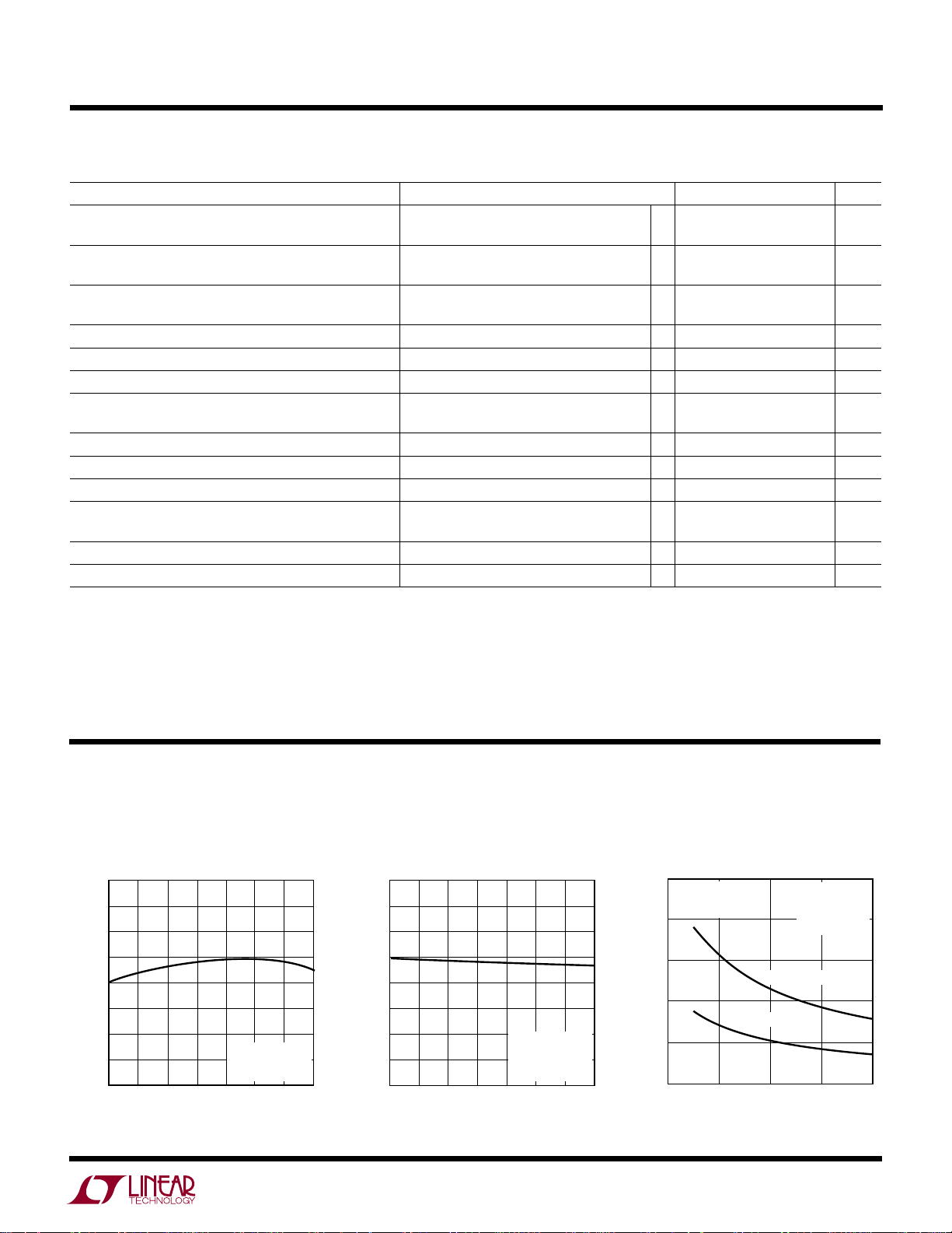
TYPICAL PERFOR A CE CHARACTERISTICS
Graphs apply to both the LT3420 and LT3420-1 unless otherwise noted.
Output Voltage in Refresh Mode,
LT3420
335
330
325
320
(V)
315
OUT
V
310
305
300
295
–50
050
–25 25 75 125
TEMPERATURE (°C)
FIGURE 1 CIRCUIT
V
CC
V
BAT
= 3.3V
= 3.3V
100
3420 G01
Output Voltage in Refresh Mode,
LT3420
335
330
325
320
(V)
315
OUT
V
310
305
300
295
2.5
FIGURE 1 CIRCUIT
V
CC
V
BAT
TA = 25°C
4.03.53.0 5.55.04.5 6.0
VIN (V)
= V
= V
pin.
FB
guaranteed by design and/or correlation
CESAT
Charge Time, LT3420
10
FIGURE 1 CIRCUIT
UNLESS OTHERWISE
NOTED.
8
6
TIME (s)
4
C
= 100µF
OUT
IN
IN
3420 G02
2
0
2
V
CHARGED
OUT
FROM
50V TO 320V
= 25°C
T
A
C
= 220µF
OUT
453
V
(V)
BAT
6
3420 G03
3420fb
3
LT3420/LT3420-1
TEMPERATURE (°C)
–50
CURRENT (mA)
100
3420 G09
050
60
55
50
45
40
35
30
25
20
–25 25 75 125
TEMPERATURE (°C)
–50
CURRENT (mA)
100
3420 G12
050
35
30
25
20
15
10
5
–25 25 75 125
UW
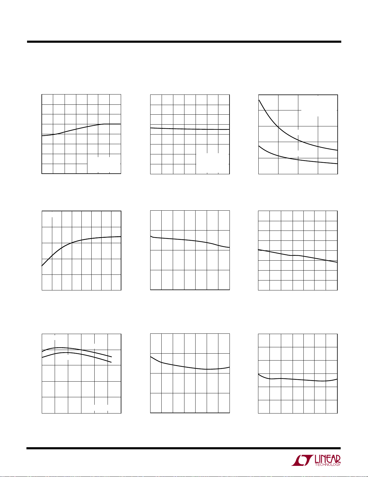
TYPICAL PERFOR A CE CHARACTERISTICS
Graphs apply to both the LT3420 and LT3420-1 unless otherwise noted.
Output Voltage in Refresh Mode,
LT3420-1
335
330
325
320
(V)
315
OUT
V
310
305
300
295
–50
050
–25 25 75 125
TEMPERATURE (°C)
FIGURE 2 CIRCUIT
V
CC
V
BAT
Charge Pin Input Current
10
TA = 25°C
8
6
4
CURRENT (µA)
2
= 3.3V
= 3.3V
100
3420 G04
Output Voltage in Refresh Mode,
LT3420-1
335
330
325
320
(V)
315
OUT
V
310
305
300
295
2.5
FIGURE 2 CIRCUIT
V
V
TA = 25°C
VIN (V)
CC
BAT
Primary Current Limit, LT3420
1.7
1.5
1.3
CURRENT (A)
1.1
= V
IN
= V
IN
5.03.0 4.03.5 4.5 6.0
5.5
3420 G05
Charge Time, LT3420-1
10
8
6
TIME (s)
4
2
0
C
2
3
OUT
C
OUT
= 40µF
V
BAT
FIGURE 2 CIRCUIT
CHARGED
V
OUT
FROM 50V TO 320V
= 25°C
T
A
= 100µF
4
(V)
Secondary Current Limit, LT3420
5
6
3420 G06
4
0
2
34
CHARGE PIN VOLTAGE (V)
6
57 10
Efficiency of Figure 1 Circuit,
LT3420
90
TA = 25°C
V
OUT
VIN = 5V
(V)
80
VIN = 3.3V
70
60
EFFICIENCY (%)
50
40
50 150 350250
100 200 300
VCC = V
89
3420 G07
= V
BAT
IN
3420 G10
0.9
–25 25 75
–50
0
TEMPERATURE (°C)
50
Primary Current Limit, LT3420-1
1.2
1.1
1.0
CURRENT (A)
0.9
0.8
–25 25 75
–50
0
TEMPERATURE (°C)
50
100
100
125
3420 G08
Secondary Current Limit, LT3420-1
125
3420 G11
3420fb
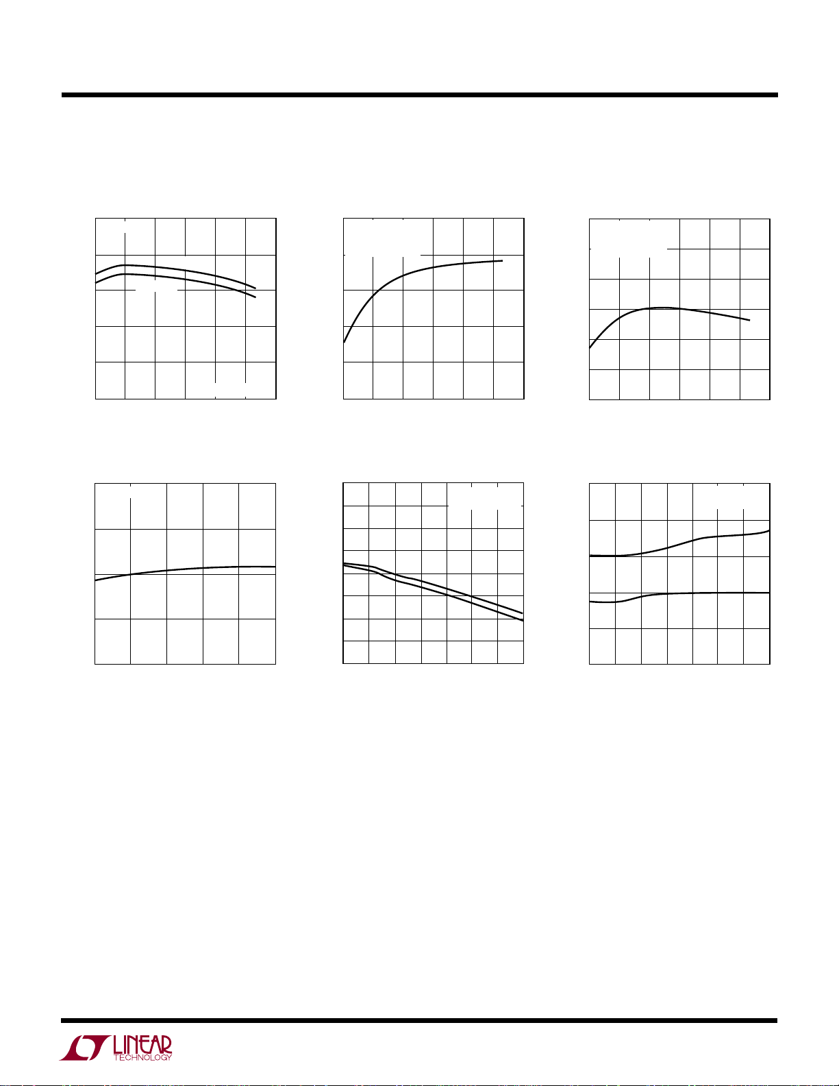
UW
TEMPERATURE (°C)
–50
V
BAT
PIN VOLTAGE (V)
100
3420 G18
050–25 25 75 125
2.0
1.8
1.6
1.4
1.2
1.0
V
+
V
–
ENABLE VOLTAGE
IS HYSTERETIC
TYPICAL PERFOR A CE CHARACTERISTICS
Graphs apply to both the LT3420 and LT3420-1 unless otherwise noted.
Efficiency for Figure 2 Circuit,
LT3420-1 Input Current, LT3420
90
TA = 25°C
80
70
60
EFFICIENCY (%)
50
40
50 150 350250
140
120
100
80
QUIESCENT CURRENT (µA)
60
2.5
VIN = 3.3V
100 200 300
V
TA = 25°C
4.0 7.0
5.5 8.5
VIN = 5V
(V)
OUT
VCC (V)
VCC = V
BAT
= V
IN
3420 G13
10
3420 G16
1000
FIGURE 1 CIRCUIT
= V
V
T
900
800
700
600
AVERAGE INPUT CURRENT (mA)
500
50 150 350250
V
2.6
2.5
2.4
2.3
2.2
2.1
PIN VOLTAGE (V)
CC
V
2.0
1.9
1.8
–50
= 3.3V
CC
BAT
= 25°C
A
100 200 300
V
OUT
Minimum Operating VoltageQuiescent Current in Refresh Mode V
CC
–
V
050
–25 25 75 125
TEMPERATURE (°C)
(V)
ENABLE VOLTAGE
IS HYSTERETIC
+
V
100
3420 G14
3420 G17
LT3420/LT3420-1
Input Current, LT3420-1
600
FIGURE 2 CIRCUIT
= V
V
550
T
500
450
400
AVERAGE INPUT CURRENT (mA)
350
300
50
= 3.3V
CC
BAT
= 25°C
A
150 200 250
100
Minimum Operating Voltage
BAT
V
(V)
OUT
300 350
3420 G15
3420fb
5

LT3420/LT3420-1
U
UU
PI FU CTIO S
R
(Pin 1): Reference Resistor Pin. Place a resistor (R2)
REF
from the R
(Pin 2): Battery Voltage Input. This pin should be
V
BAT
connected to the power supply or battery, which supplies
power to transformer T1. Must be locally bypassed.
RFB (Pin 3): Feedback Resistor Pin. Place a resistor (R1)
from the SW pin to the R
following formula:
R
1
=++
R
1
=++
V
OUT
N: Transformer Turns Ratio
R
SEC
VD: Diode Forward Voltage Drop
pin to GND. 2k is recommended.
REF
pin. Set R1 according to the
FB
R
2
2
N
R
2
2
N
: Desired Output Voltage
: Transformer Secondary Resistance
RNV V
14 2
(. • ) ( )
[]
()( )
[]
SEC OUT D
RNV V
SEC OUT D
2
(LT3420)
(LT3420-1)
GND (Pin 5): Ground. Tie directly to local ground plane.
SW (Pin 6): Switch Pin. This is the collector of the internal
NPN power switch. Minimize the metal trace area connected to this pin to minimize EMI.
SEC (Pin 7): Transformer Secondary Pin. Tie one end of
the transformer secondary to this pin. Take care to use the
correct phasing of the transformer (Refer to Figures 1
and 2).
DONE (Pin 8): Done Output Pin. Open collector NPN
output. DONE is pulled low whenever the chip is delivering
power to the output and goes high when power delivery
stops.
CHARGE (Pin 9): Charge Pin. Drive CHARGE high (1.5V or
more) to commence charging of the output capacitor.
Drive to 0.2V or less to put the part in shutdown mode.
CT (Pin 10): Refresh Timer Capacitor Pin. Place a capacitor
from the CT pin to GND to set the refresh timer sample rate
according to the following formula:
R2: Resistor from the R
Choice
VCC (Pin 4): Input Supply Pin. Must be locally bypassed
with a 4.7µF or larger ceramic capacitor.
Pin to GND. 2k is a Typical
REF
CT = 2.5 • 10–6 • t
t
REFRESH
EXPOSED PAD (Pin 11) (DD Package only): GND. Must be
soldered to local ground plane on PCB.
: Desired Refresh Period in Seconds.
REFRESH
6
3420fb

W
BLOCK DIAGRA S
V
BAT
DONE
8
REFRESH
10
C3
CHARGE
V
CC
C2
CT
TIMER
ENABLE
QQ
MASTER
LATCH
S
ONE-
9
SHOT
CHIP
4
V
ENABLE
CC
Q5 Q3
BLOCK
ENABLE
R
LT3420/LT3420-1
T1
1:12
C1
R1
R2
R
V
BAT
2 3 1 6
D3
R
FB
REF
R
Q
S
DRIVER
PRIMARY
SW
Q1
D1
SECONDARY
PHOTOFLASH
CAPACITOR
+
Q2
+
A3 A2
–
REFERENCE
ONE-
SHOT
1V
POWER DELIVERY BLOCK
A1
–
Q4
–
+
20mV
+
10mV
+
0.014Ω
–
5
GND
0.25Ω
LT3420
7
SEC
3420 F03
–
V
OUT
+
C4
CHARGE
V
Figure 3. Block Diagram, LT3420
T1
V
BAT
C1
R1
R2
DONE
8
REFRESH
10
CT
C3
CC
C2
TIMER
ENABLE
QQ
MASTER
LATCH
S
ONE-
9
SHOT
CHIP
4
V
ENABLE
CC
Q5 Q3
BLOCK
ENABLE
R
A3 A2
R
V
BAT
2 3 1 6
D3
R
FB
REF
R
Q
S
DRIVER
+
Q2
+
–
REFERENCE
ONE-
SHOT
1V
POWER DELIVERY BLOCK
A1
20mV
–
+
–
Q4
–
10mV
+
+
–
PRIMARY
SW
Q1
0.02Ω
0.66Ω
LT3420-1
1:10
5
GND
7
SEC
3420 F04
D1
SECONDARY
PHOTOFLASH
CAPACITOR
V
OUT
+
C4
Figure 4. Block Diagram, LT3420-1
3420fb
7
LT3420/LT3420-1
U
OPERATIO
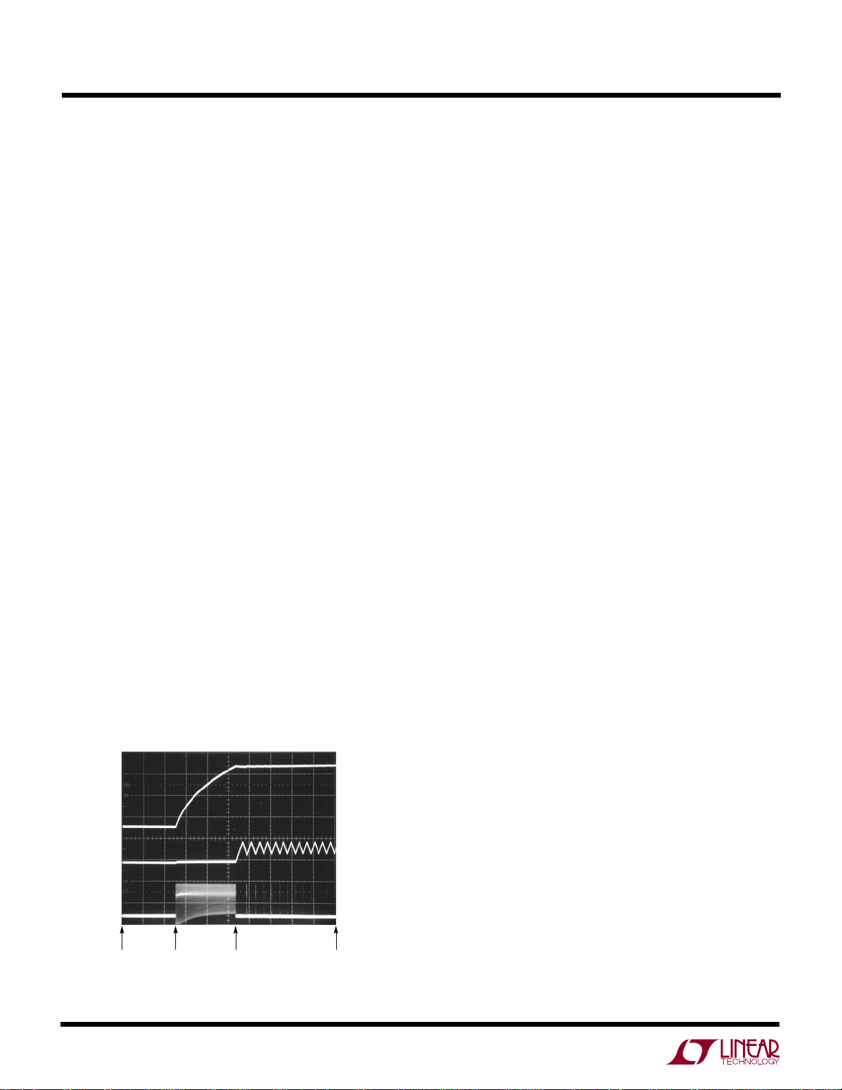
Overview
The following text focuses on the operation of the LT3420.
The operation of the LT3420-1 is nearly identical with the
differences discussed at the end of this section.
The LT3420 uses an adaptive on-time/off-time control
scheme to provide excellent efficiency and precise control
of switching currents. Please refer to Figure 3 for the following overview of the part’s operation. At any given instant,
the master latch determines which mode the LT3420 is in:
“charging” or “refresh”. In charging mode, the circuitry
enclosed by the smaller dashed box is enabled, providing
power to charge photoflash capacitor C1. The output voltage is monitored via the flyback pulse on the primary of the
transformer. When the target output voltage is reached, the
charging mode is terminated and the part enters the refresh
mode. In refresh mode, the power delivery block is disabled,
reducing quiescent current, while the refresh timer is enabled. The refresh timer simply generates a user programmable delay, after which the part reenters the charging
mode. Once in the charging mode, the LT3420 will again
provide power to the output until the target voltage is
reached. Figure 5 is an oscillograph photo showing both the
initial charging of the photoflash capacitor and the subsequent refresh action. The upper waveform is the output
voltage. The middle waveform is the voltage on the CT pin.
The lower waveform shows the input current. The mode of
the part is indicated below the photo.
The user can defeat the refresh timer and force the part
into charging mode by toggling the CHARGE pin
V
OUT
100V/DIV
V
CT
1V/DIV
I
IN
1A/DIV
MODE
SHUTDOWN
Shutdown, Charging and Refresh of Photoflash Capacitor
CHARGING
1s/DIV
REFRESH
3420 F05
(high→low→high). The low to high transition on the
CHARGE pin fires a one-shot that sets the master latch,
putting the part in charging mode. Bringing CHARGE low
puts the part in shutdown. The refresh timer can be
programmed to wait indefinitely by simply grounding the
pin. In this configuration, the LT3420 will only reenter
C
T
the charging mode by toggling the CHARGE pin.
Power Delivery Block
The power delivery block consists of all circuitry enclosed
by the smaller dashed box in Figure 3. This circuit block
contains all elements needed for charging and output
voltage detection. To better understand the circuit operation, follow the subsequent description of one cycle of
operation and refer to Figure 6. Assume that initially there
is no current in the primary or secondary of the transformer, so the output of comparator A1 is low, while that
of A2 is high (note the small offset voltages at the inputs
of A1 and A2). The SR latch is thus set and the power NPN
switch, Q1, is turned on. Current increases linearly in the
primary of the transformer at a rate determined by the V
BAT
voltage and the primary inductance of the transformer. As
the current builds up, the voltage across the 14mΩ
resistor increases. When this voltage exceeds the 20mV
offset voltage of A1, the output of A1 goes high, resetting
the SR latch and turning off Q1. The current needed to
reset the latch is approximately 1.4A (~20mV/14mΩ).
When Q1 turns off, the secondary side current quickly
jumps from zero current to the primary side current divided by N (the turns ratio of transformer T1). In this example, the peak secondary current is 116mA (1.4A/12).
Diode D1 now conducts, providing power to the output.
Since a positive voltage exists across the secondary winding of the transformer, the secondary current decreases
linearly at a rate determined by the secondary inductance
and the output voltage (neglecting the diode voltage drop).
When the secondary side current drops below 40mA
(10mV/0.25Ω), the output of A2 goes high, setting the SR
latch and turning on Q1. The initial primary current is simply the minimum secondary current times N, in this case
0.48A (40mA • 12) . Q1 will now remain on until the primary current again reaches 1.4A. This cycle of operation
repeats itself, automatically adjusting the On and Off timesFigure 5. Demonstrating 3 Operating Modes of LT3420:
3420fb
8

OPERATIO
LT3420/LT3420-1
U
I
SW
1A/DIV
I
SEC
200mA/DIV
V
SW
20V/DIV
2µs/DIV
Figure 6a. Switching Waveforms with
V
= 100V, VCC = V
OUT
BAT
= 3.3V
3420 F06a
of Q1 so that the peak current of Q1 is 1.4A and the minimum secondary current is 40mA (typical values).
The previously described charging cycle must be halted
when the output voltage reaches the desired value. The
LT3420 monitors the output voltage via the flyback pulse
on the SW pin. When Q1 turns off, the secondary side
conducts current turning on diode D1. Since the diode is
conducting and the SEC pin is at nearly ground, the voltage
across the secondary is nearly equal to V
across the primary is therefore close to V
proportional to V
pin. The current flows out of the R
/N flows through R1 and into the R
OUT
pin through a resis-
REF
. The voltage
OUT
/N. A current
OUT
FB
tor creating a ground referred voltage. When this voltage
exceeds an internal 1V reference voltage, the output of
comparator A3 goes high which resets the master latch. The
Q output of the master latch goes low, disabling the entire
power delivery block and enabling the refresh timer.
Leakage Spike Blanking
I
SW
1A/DIV
I
SEC
200mA/DIV
V
SW
20V/DIV
2µs/DIV
Figure 6b. Switching Waveforms with
= 300V, VCC = V
V
OUT
BAT
= 3.3V
3420 F06b
C3, from its initial voltage towards 1V. When the voltage
on C3 reaches 1V, the polarity of the current source changes
and 2.5µA discharges C3. When the voltage on C3 reaches
0.5V, the refresh timer sends a set pulse to the master latch,
which puts the LT3420 into the charging mode.
Interface/Control
The CHARGE pin serves two functions. The first is to
enable or shutdown the part depending on the level of the
pin (high = enable, low = shutdown). The second is to
force the part into the charging mode (low→high transition). The LT3420 also has a DONE pin, which signals
whether or not the part is done charging the photoflash
capacitor. The DONE pin is an open collector NPN switch
(Q5) so an external pull-up resistor is needed. Whenever
the part is in charging mode, DONE will be low. DONE will
go high when the charging mode is complete. Both the
CHARGE and DONE pins can be easily interfaced to a
microprocessor in a digital or film camera.
Another function of the LT3420 is leakage spike blanking
when the power switch, Q1, turns off. Right after Q1 turns
off, a one-shot turns on Q2 for 200ns (typ). With Q2 on,
comparator A3 is disabled. This function may prevent A3
from false tripping on the leakage inductance spike on the
SW pin. In practice, the PNP transistor Q3 filters out the
leakage spike.
Refresh Timer
When the refresh timer is enabled, a 2.5µA current source
is switched on, charging up the external timing capacitor,
LT3420-1 Differences
The LT3420-1 has different primary and secondary current limit levels. The primary current limit level of the
LT3420-1 is 1A (typ) and the secondary current limit is
15mA (typ). The LT3420-1 has no leakage spike blanking
which causes no problems since the PNP transistor, Q3,
provides adequate filtering. Finally, the breakdown voltage
of the SW pin of the LT3420-1 is higher at 50V.
3420fb
9

LT3420/LT3420-1
WUUU
APPLICATIO S I FOR ATIO
COMPONENT SELECTION
Choosing the Right Transformer
The flyback transformer plays a key role in any LT3420/
LT3420-1 application. A poorly designed transformer can
result in inefficient operation. Linear Technology Corporation has worked with a number of transformer manufacturers to develop specific transformers for use with the
LT3420/LT3420-1. These predesigned transformers are
sufficient for a large majority of the applications that may
be encountered. In some cases, the reader may choose to
design his own transformer or may simply be curious about
the issues involved in designing the transformer. The following is a brief discussion of the issues relating to transformer design.
Transformer Turns Ratio
The turns ratio for the transformer, N, should be high
enough so that the absolute maximum voltage rating for
the NPN power switch is not exceeded. When the power
switch turns off, the voltage on the collector of the switch
(SW Pin) will “fly” up to the output voltage divided by N
plus the battery voltage (neglecting the voltage drop
across the rectifying diodes). This voltage should not
exceed the 38V (LT3420) or 50V (LT3420-1) breakdown
rating of the power switch.
Choose the minimum N by the following formula.
Transformer Primary Inductance
A flyback transformer needs to store substantial amounts
of energy in the core during each switching cycle. The
transformer, therefore, will generally require an air gap.
The use of an air gap in the core makes the energy storage
ability, or inductance, much more stable with temperature
and variations in the core material. Most core manufacturers will supply standard sizes of air gaps with a given type
of core, resulting in different A
values. AL is the induc-
L
tance of a particular core per square turns of winding. To
get a certain inductance, simply divide the desired inductance by the A
value and take the square root of the result
L
to find the number of turns needed on the primary of the
transformer.
The LT3420/LT3420-1 detect the output voltage via the
flyback pulse on the SW pin. Since this can only occur
while the power switch is off, an important criteria is that
the value of the primary inductance of the transformer be
larger than a certain minimum value. The switch off time
should be 500ns or larger for the LT3420 and 350ns or
larger for the LT3420-1. The minimum inductance can be
calculated with the following formula:
9
–
••
L
L
500 10
≥
PRI
PRI
•( . – . )
NN
14 004
••
350 10
≥−
•(.–. )
NN
10 0015
V
OUT
()
LT
3420
9
–
V
OUT
()
LT
3420 1
V
N
N
MIN
MIN
OUT
≥
≥−
38
50
–
V
–
V
OUT
V
LT
3420
()
BAT
LT
3420 1
()
BAT
For an LT3420 design, a 5V battery voltage and a 330V
output results in a N
of 10 so a turns ratio of 10 or greater
MIN
should be used.
10
V
: Target Output Voltage
OUT
N: Transformer Turns Ratio
Transformer Leakage Inductance
The leakage inductance of the transformer must be carefully minimized for both proper and efficient operation of
the part. The DC voltage rating of the SW pin on the LT3420
is 38V while on the LT3420-1 it is 50V. These ratings are
for DC blocking voltages only and additional precautions
3420fb

WUUU
APPLICATIO S I FOR ATIO
LT3420/LT3420-1
must be taken into account for the dynamic blocking
voltage capabilities of the LT3420/LT3420-1. The dynamic
blocking voltage capability of both parts is 38V.
Table 1 summarizes the various breakdown voltages of the
SW pin for both parts.
Table 1. SW Pin Voltage Ratings
PART SW PIN DC RATING SW PIN DYNAMIC RATING
LT3420 38V 38V
LT3420-1 50V 38V
Figure 7 shows what to examine in a new transformer
design to determine if the specifications for the SW pin are
met.
The first leakage inductance spike labeled “A” must not
exceed the dynamic rating of the SW pin. If it does exceed
the rating, then the transformer leakage inductance must
be lowered. The flyback waveform after the initial spike
labeled “B” must not exceed the DC rating of the SW pin.
If it does exceed the rating, then the turns ratio of the
transformer must be lowered. In measuring the voltage on
the SW pin, care must be taken in minimizing the ground
loop of the voltage probe. Careless probing will result in
inaccurate readings.
Note also the magnitude of the initial current spike in the
primary of the transformer labeled “C” when the power
switch turns on. If the leakage inductance is lowered to a
very low level, the internal capacitances of the transformer
will be high. This will result in the initial spike of current in
the primary becoming excessively high. The level of “C”
should be kept to 4A or less in a typical design for both the
LT3420 and LT3420-1. Please note that by inserting a loop
of wire in the primary to measure the primary current, the
leakage inductance of the primary will be made artificially
high. This may result in erroneous voltage measurements
on the SW pin.
The measurements shown in Figure 7 should be made
with both V
OUT
and V
at the maximum levels for the
BAT
given application. This results in the highest voltage and
current stress on the SW pin.
Transformer Secondary Capacitance
The total capacitance of the secondary should be minimized for both efficient and proper operation of the LT3420/
LT3420-1. Since the secondary of the transformer undergoes large voltage swings (approaching 600V
P-P
), any
capacitance on the secondary can severely affect the
MUST BE LESS THAN 4A
FOR BOTH THE LT3420
AND LT3420-1
“C”
I
PRI
0A
MUST BE LESS THAN 38V
FOR THE LT3420
“B”
“A”
V
SW
0V
Figure 7. New Transformer Design Check (Not to Scale)
MUST BE LESS THAN 50V
FOR THE LT3420-1
MUST BE LESS THAN 38V
FOR BOTH THE LT3420
AND LT3420-1
3420 F07
3420fb
11

LT3420/LT3420-1
U
WUU
APPLICATIO S I FOR ATIO
efficiency of the circuit. In addition, the effective capacitance on the primary is largely dominated by the actual
secondary capacitance. This is simply a result of any
secondary capacitance being multiplied by N2 when reflected to the primary. Since N is generally 10 or higher, a
small capacitance of 10pF on the secondary is 100 times
larger, or 1.0nF, on the primary. This capacitance forms a
resonant circuit with the primary leakage inductance of the
transformer. As such, both the primary leakage inductance and secondary side capacitance should be minimized.
Table 2 shows various predesigned transformers along
with relevant parameters. Contact the individual transformer manufacturer for additional information or
customization.
Table 2a. Predesigned Transformers, LT3420
PART RATIO (µH) LxWxH (mm) VENDOR
SRW10EPC 1:12 24 10.9x10.8x5.2 TDK
-U01H003 (847) 803-6100
6375-T108 1:12 15 10.8x9.5x3.6 Sumida
SBL-6.4 1:12 17.5 10.3x6.4x5.2 Kijima Musen
Table 2b. Predesigned Transformers, LT3420-1
PART RATIO (µH) LxWxH (mm) VENDOR
SBL-5.6S-2 1:10 15 5.6x8.5x3.0 Kijima Musen
LDT565630T 1:10.2 14.5 5.8x5.8x3.0 TDK
-002 (847) 803-6100
TURNS L SIZE
www.components.tdk.com
(847) 956-0666
www.sumida.com
852-2489-8266
kijimahk@netvigator.com
TURNS L SIZE
852-2489-8266
kijimahk@netvigator.com
www.components.tdk.com
DIODE SELECTION
The rectifying diode(s) should be low capacitance type
with sufficient reverse voltage and forward current ratings. The peak reverse voltage that the diode(s) will see is
approximately:
V
≈ +
PK-R
VNV
()
(• )•.165
OUT BAT
The peak current of the diode is simply:
14
.
I
PK-SEC
I
PK-SEC
For the circuit of Figure 1 with V
and I
PK-SEC
A
=
3420
()
LT
N
10
.
A
= −
3420 1
()
LT
N
of 3.3V, V
BAT
PK-R
is 590V
is 116mA. Table 3 shows various diodes that
can work with the LT3420/LT3420-1. These are chosen for
low capacitance and high reverse blocking voltage. Use
the appropriate number of diodes to achieve the necessary
reverse breakdown voltage.
Table 3
PART VOLTAGE (V) (pF) VENDOR
GSD2004S 2x300 5 Vishay
(Dual diode) (402) 563-6866
BAS21 250 1.5 Philips Semiconductor
(Single diode) (800) 234-7381
MMBD3004S 2x300 5 Diodes Inc.
MAX REVERSE CAPACITANCE
www.vishay.com
www.philips.com
(805) 446-4800
www.diodes.com
12
3420fb

WUUU
APPLICATIO S I FOR ATIO
LT3420/LT3420-1
CAPACITOR SELECTION
The V
and VCC decoupling capacitors should be multi-
BAT
layer ceramic type with X5R or X7R dielectric. This insures
adequate decoupling across wide ambient temperature
ranges. A good quality ceramic capacitor is also recommended for the timing capacitor on the CT pin. Avoid Y5V
or Z5U dielectrics.
Selectively Disabling the LT3420/LT3420-1
The LT3420/LT3420-1 can be disabled at any time, even
during the charge phase. This may be useful when a digital
camera enters a sensitive data acquisition phase. Figure 8
illustrates this feature. Midway through the charge cycle,
the CHARGE pin is brought low, which disables the part.
After the sensitive data operation is complete, the CHARGE
pin is brought high and the charging operation continues.
Measuring Efficiency
Measuring the efficiency of a circuit designed to charge
large capacitive loads is a difficult issue, particularly with
photoflash capacitors. The ideal way to measure the
efficiency of a capacitor charging circuit would be to find
the energy delivered to the output capacitor (0.5 • C • V2)
and divide it by the total input energy. This method does
not work well here because photoflash capacitors are far
from ideal. Among other things, they have relatively high
leakage currents, large amounts of dielectric absorption,
and significant voltage coefficients. A much more accurate, and easier, method is to measure the efficiency as a
function of the output voltage. In place of the photoflash
capacitor, use a smaller, high quality capacitor, reducing
errors associated with the non-ideal photoflash capacitor.
Using an adjustable load, the output voltage can be set
anywhere between ground and the maximum output
voltage. The efficiency is measured as the output power
(V
• I
OUT
) divided by the input power (VIN • IIN). This
OUT
method also provides a good means to compare various
charging circuits since it removes the variability of the
photoflash capacitor from the measurement. The total
efficiency of the circuit, charging an ideal capacitor, would
be the time average of the given efficiency curve, over time
as V
changes.
OUT
Adjustable Input Current
With many types of modern batteries, the maximum
allowable current that can be drawn from the battery is
limited. This is generally accomplished by active circuitry
or a polyfuse. Different parts of a digital camera may
require high currents during certain phases of operation
and very little at other times. A photoflash charging circuit
should be able to adapt to these varying currents by
drawing more current when the rest of the camera is
drawing less, and vice-versa. This helps to reduce the
charge time of the photoflash capacitor, while avoiding the
V
CHARGE
V
OUT
50V/DIV
CHARGE
NO
CHARGE
Figure 8. Halting the Charge Cycle at Any Time
0.5s/DIV
3420 F08
5V/
DIV
3420fb
13
LT3420/LT3420-1
WUUU
APPLICATIO S I FOR ATIO
risk of drawing too much current from the battery. The
input current to the LT3420/LT3420-1 circuit can be
adjusted by driving the CHARGE pin with a PWM (pulse
width modulation) signal. The microprocessor can adjust
the duty cycle of the PWM signal to achieve the desired
level of input current. Many schemes exist to achieve this
function. Once the target output voltage is reached, the
PWM signal should be halted to avoid overcharging the
photoflash capacitor, since the signal at the CHARGE pin
overrides the refresh timer.
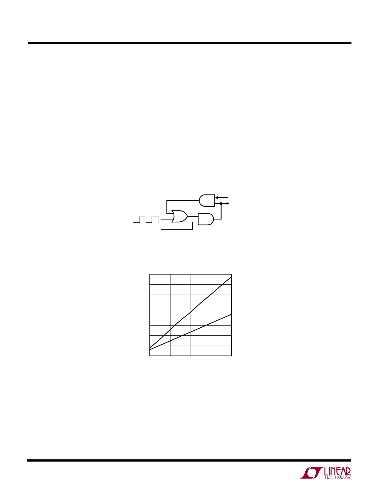
A simple method to achieve adjustable input current is
shown in Figure 9. The PWM signal has a frequency of
1kHz PWM
SIGNAL
ON
Figure 9. Simple Logic for Adjustable Input Current
A2
1kHz. When ON is logic high, the circuit is enabled and the
CHARGE pin is driven by the PWM signal. When the target
output voltage is reached, DONE goes high while CHARGE
is also high. The output of A1 goes high, which forces
CHARGE high regardless of the PWM signal. The part is
now in the Refresh mode. Once the refresh period is over,
the DONE pin goes low, allowing the PWM signal to drive
the CHARGE pin once again. This function can be easily
implemented in a microcontroller. Figure 10 shows the
input current for the LT3420 and LT3420-1 as the duty
cycle of the PWM signal is varied.
A1
A3
DONE
CHARGE
TO
LT3420
CIRCUIT
3420 F09
800
600
400
INPUT CURRENT (mA)
200
0
10
LT3420
LT3420-1
30 50 70
DUTY CYCLE (%)
90
3420 F10
Figure 10. Input Current as Duty Cycle is Varied
14
3420fb

WUUU
APPLICATIO S I FOR ATIO
LT3420/LT3420-1
BOARD LAYOUT
The high voltage operation of the LT3420/LT3420-1
demands careful attention to board layout. You will not
get advertised performance with careless layout. Figures 11 and 12 show the recommended component
placement. Keep the area for the high voltage end of the
secondary as small as possible. Note the larger than
minimum spacing for all high voltage nodes. This is
R2
V
CC
GND
C2
C1
necessary to meet the breakdown specifications for the
circuit board. If the Photoflash capacitor is placed far
from the LT3420/LT3420-1 circuit, place a small (20nF50nF) ceramic capacitor with sufficient voltage rating
close to the part. This insures adequate bypassing.
Remember that LETHAL VOLTAGES ARE PRESENT in
this circuit. Use caution when working with the circuit.
CHARGE DONE
C3
PHOTOFLASH
CAPACITOR
–
+
R1
T1
V
OUT
V
V
GND
V
BAT
BAT
D1B
D1A
3420 F11
Figure 11. Suggested Layout (MS10 Package)
CHARGE DONE
R2
CC
C2
C1
C3
PHOTOFLASH
CAPACITOR
–
+
R1
T1
V
OUT
D1B
D1A
Figure 12. Suggested Layout (DD Package)
3420 F12
3420fb
15

LT3420/LT3420-1
TYPICAL APPLICATIO S
Professional Charger uses Multiple LT3420 Circuits in Parallel to Charge Large Photoflash Capacitors Quickly
U
DANGER HIGH VOLTAGE
OPERATION BY HIGH VOLTAGE
TRAINED PERSONEL ONLY
V
CC
R3
100k
Q1
2N3904
C1, C2, C4, C5, C6, C7: 4.7µF, X5R or X7R, 10V
T1-T3: TDK SRW10EPC-U01H003 FLYBACK TRANSFORMER
D1-D3: VISHAY GSD2004S SOT-23
DUAL DIODE. DIODES CONNECTED IN SERIES
Q1: 2N3904 OR EQUIVALENT
* CAN CHARGE ANY SIZE PHOTOFLASH CAPACITOR
** USE AS MANY SLAVE CHARGERS AS NEEDED.
V
BAT
1.8V TO 6V
V
2.5V TO 10V
CHARGE
V
BAT
R4
100k
V
BAT
V
D1
C1
4.7µF
V
BATRFB
CC
CC
C2
4.7µF
0.1µF
C4
4.7µF
C5
4.7µF
C6
4.7µF
C7
4.7µF
4
9
8
C3
4
9
8
4
9
8
V
CC
CHARGE
DONE
C
V
BATRFB
V
CC
CHARGE
DONE
C
V
BATRFB
V
CC
CHARGE
DONE
C
5, 6 8
3, 4
R1
52.3k
2
36
LT3420
R
T
10 5
2
T
10 5
2
T
10 5
GND
5, 6
3, 4
36
LT3420
R
GND
5, 6
3, 4
36
LT3420
R
GND
SW
SEC
REF
SW
SEC
REF
SW
SEC
REF
T1
1:12
1
7
MASTER
CHARGER
1
R2
2k
8
T2
1:12
1
7
SLAVE**
CHARGER
1
8
T3
1:12
1
1
7
SLAVE**
CHARGER
1
3420 TA01
D2
D3
+
320V
650µF*
350V
PHOTOFLASH
CAPACITOR
16
3420fb

U
TYPICAL APPLICATIO S
LT3420 Photoflash Charging Circuit Uses Small Transformer
DANGER HIGH VOLTAGE
OPERATION BY HIGH VOLTAGE
TRAINED PERSONEL ONLY
1.8V TO 5V
2.5V TO 10V
CHARGE
C1: 4.7µF, X5R or X7R, 6.3V
C2: 4.7µF, X5R or X7R, 10V
C4: RUBYCON 220µF PHOTOFLASH CAPACITOR
D1: VISHAY GSD2004S SOT-23
DUAL DIODE. DIODES CONNECTED IN SERIES
T1: KIJIMA MUSEN SBL-6.4
* MAXIMUM AMBIENT TEMPERATURE OF 60°C DICTATED BY TRANSFORMER
V
BAT
V
DONE
LT3420/LT3420-1
T1*
1:12
3
LT3420
C3
0.1µF
R1
47.5k
2
1
SW
SEC
R
GND
REF
632
1
5
7
PHOTOFLASH
CAPACITOR
R2
2k
D1
220µF
330V
C1
4.7µF
V
BATRFB
CC
C2
4.7µF
9
8
4
V
CC
CHARGE
DONE
C
T
10 5
300V
C4
+
3420 TA02
90
VCC = V
80
70
60
EFFICIENCY (%)
50
40
50
100
Efficiency
= V
BAT
IN
VIN = 3.3V
150 200 250
V
OUT
VIN = 5V
300 350
(V)
3420 TA03
3420fb
17
LT3420/LT3420-1
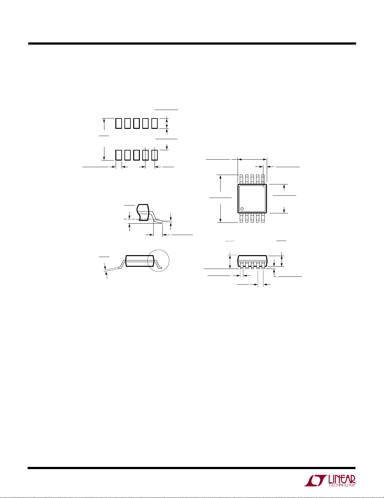
PACKAGE DESCRIPTIO
U
MS Package
10-Lead Plastic MSOP
(Reference LTC DWG # 05-08-1661)
0.889 ± 0.127
± .005)
(.035
5.23
(.206)
MIN
0.305
± 0.038
± .0015)
(.0120
TYP
RECOMMENDED SOLDER PAD LAYOUT
0.254
(.010)
GAUGE PLANE
0.18
(.007)
NOTE:
1. DIMENSIONS IN MILLIMETER/(INCH)
2. DRAWING NOT TO SCALE
3. DIMENSION DOES NOT INCLUDE MOLD FLASH, PROTRUSIONS OR GATE BURRS.
MOLD FLASH, PROTRUSIONS OR GATE BURRS SHALL NOT EXCEED 0.152mm (.006") PER SIDE
4. DIMENSION DOES NOT INCLUDE INTERLEAD FLASH OR PROTRUSIONS.
INTERLEAD FLASH OR PROTRUSIONS SHALL NOT EXCEED 0.152mm (.006") PER SIDE
5. LEAD COPLANARITY (BOTTOM OF LEADS AFTER FORMING) SHALL BE 0.102mm (.004") MAX
3.20 – 3.45
(.126 – .136)
DETAIL “A”
DETAIL “A”
0.50
(.0197)
BSC
0° – 6° TYP
0.53 ± 0.152
(.021 ± .006)
SEATING
PLANE
3.00 ± 0.102
(.118 ± .004)
(NOTE 3)
4.90 ± 0.152
(.193 ± .006)
(.043)
0.17 – 0.27
(.007 – .011)
TYP
1.10
MAX
12
0.50
(.0197)
BSC
8910
3
7
6
45
0.497 ± 0.076
(.0196 ± .003)
REF
3.00 ± 0.102
(.118 ± .004)
(NOTE 4)
0.86
(.034)
REF
0.127
± 0.076
(.005 ± .003)
MSOP (MS) 0603
18
3420fb

PACKAGE DESCRIPTIO
LT3420/LT3420-1
U
DD Package
10-Lead Plastic DFN (3mm × 3mm)
(Reference LTC DWG # 05-08-1699)
0.675 ±0.05
3.50 ±0.05
1.65 ±0.05
(2 SIDES)2.15 ±0.05
PACKAGE
OUTLINE
0.25 ± 0.05
RECOMMENDED SOLDER PAD PITCH AND DIMENSIONS
PIN 1
TOP MARK
(SEE NOTE 6)
0.200 REF
NOTE:
1. DRAWING TO BE MADE A JEDEC PACKAGE OUTLINE M0-229 VARIATION OF (WEED-2).
CHECK THE LTC WEBSITE DATA SHEET FOR CURRENT STATUS OF VARIATION ASSIGNMENT
2. DRAWING NOT TO SCALE
3. ALL DIMENSIONS ARE IN MILLIMETERS
4. DIMENSIONS OF EXPOSED PAD ON BOTTOM OF PACKAGE DO NOT INCLUDE
MOLD FLASH. MOLD FLASH, IF PRESENT, SHALL NOT EXCEED 0.15mm ON ANY SIDE
5. EXPOSED PAD SHALL BE SOLDER PLATED
6. SHADED AREA IS ONLY A REFERENCE FOR PIN 1 LOCATION ON THE
TOP AND BOTTOM OF PACKAGE
0.50
BSC
2.38 ±0.05
(2 SIDES)
3.00 ±0.10
(4 SIDES)
0.75 ±0.05
1.65 ± 0.10
(2 SIDES)
0.00 – 0.05
R = 0.115
TYP
2.38 ±0.10
(2 SIDES)
BOTTOM VIEW—EXPOSED PAD
106
15
0.25 ± 0.05
0.50 BSC
0.38 ± 0.10
(DD10) DFN 1103
Information furnished by Linear Technology Corporation is believed to be accurate and reliable.
However, no responsibility is assumed for its use. Linear Technology Corporation makes no representation that the interconnection of its circuits as described herein will not infringe on existing patent rights.
3420fb
19

LT3420/LT3420-1
TYPICAL APPLICATIO
LT3420-1 Photoflash Circuit Uses Tiny (3mm Tall) Transformer
U
60.4k
5
8
SW
SEC
R
GND
REF
T1
1:10.2
632
4
1
7
PHOTOFLASH
CAPACITOR
1
2k
D1
100µF
330V
320V
Charge Time
10
8
C3
+
3420 TA04
6
TIME (s)
4
2
0
C
2
3
OUT
C
OUT
= 40µF
V
BAT
V
CHARGED
OUT
FROM 50V TO 320V
= 100µF
4
(V)
5
6
3420 TA05
V
BAT
1.8V TO 6V
DANGER HIGH VOLTAGE
OPERATION BY HIGH VOLTAGE
TRAINED PERSONEL ONLY
V
CC
2.5V TO 6V
CHARGE
DONE
C1, C2: 4.7µF, X5R or X7R, 6.3V
C3: RUBYCON 100µF PHOTOFLASH CAPACITOR
T1: TDK LDT565630T-002 FLYBACK TRANSFORMER
D1: VISHAY GSD2004S SOT-23
DUAL DIODE. DIODES CONNECTED IN SERIES
C1
4.7µF
C2
4.7µF
9
8
4
V
BATRFB
V
CC
CHARGE
DONE
C
LT3420-1
T
10 5
0.1µF
RELATED PARTS
PART NUMBER DESCRIPTION COMMENTS
LTC®3400/LTC3400B 600mA (ISW), 1.2MHz, Synchronous Step-Up V
DC/DC Converters I
LTC3401/LTC3402 1A/2A (ISW), 3MHz, Synchronous Step-Up V
DC/DC Converters MS Package
LTC3405/LTC3405A 300mA (I
), 1.5MHz, Synchronous Step-Down 95% Efficiency, V
OUT
DC/DC Converters I
LTC3406/LTC3406B 600mA (I
), 1.5MHz, Synchronous Step-Down 95% Efficiency, V
OUT
DC/DC Converters I
LTC3407 Dual 600mA (I
), 1.5MHz, Synchronous Step-Down 95% Efficiency, V
OUT
DC/DC Converter I
LTC3411 1.25A (I
), 4MHz, Synchronous Step-Down 95% Efficiency, V
OUT
DC/DC Converter I
LTC3425 5A (ISW), 8MHz, Multiphase Synchronous Step-Up 95% Efficiency, V
DC/DC Converter I
LTC3440/LTC3441 600mA/1A (I
), 2MHz/1MHz, Synchronous Buck-Boost 95% Efficiency, V
OUT
DC/DC Converters I
LT3464 85mA (ISW), Constant Off-Time, High Efficiency V
Step-Up DC/DC Converter with Integrated Schottky ThinSOT Package
and Output Disconnect
LTC3467 1.1A (ISW), 1.3MHz, High Efficiency Step-Up V
DC/DC Converter ThinSOT Package
LTC3468/LTC3468-1/ Photoflash Capacitor Charger in ThinSOT Fast Photoflash Charge Times; 4.6sec for LT3468, 5.5sec for
LTC3468-2 LT3468-1, 5.7sec for LT3468-2
ThinsSOT is a trademark of Linear Technology Corporation.
Linear Technology Corporation
20
1630 McCarthy Blvd., Milpitas, CA 95035-7417
(408) 432-1900 ● FAX: (408) 434-0507 ● www.linear.com
= 0.85V to 5V, V
IN
= <1µA, ThinSOTTM Package
SD
= 0.5V to 5V, V
IN
= <1µA, ThinSOT Package
SD
= <1µA, ThinSOT Package
SD
= <1µA, ThinSOT Package
SD
= <1µA, MS Package
SD
= <1µA, QFN Package
SD
= <1µA, MS Package
SD
= 2.3V to 10V, V
IN
= 2.4V to 16V, V
IN
OUT(MAX)
OUT(MAX)
= 2.7V to 6V, V
IN
= 2.5V to 5.5V, V
IN
= 2.5V to 5.5V, V
IN
= 2.5V to 5.5V, V
IN
= 0.5V to 4.5V, V
IN
= 2.5V to 5.5V, V
IN
OUT(MAX)
OUT(MAX)
= 5V, IQ = 19µA/300µA,
= 6V, IQ = 38µA, ISD = <1µA,
= 0.8V , IQ = 20µA,
OUT(MIN)
= 0.6V, IQ = 20µA,
OUT(MIN)
= 0.6V, IQ = 40µA,
OUT(MIN)
= 0.8V, IQ = 60µA,
OUT(MIN)
= 5.25V, IQ = 12µA,
OUT(MIN)
= 2.5V, IQ = 25µA,
OUT(MIN)
= 34V, IQ = 25µA, ISD = <0.5µA,
= 40V, IQ = 1.2mA, ISD = <1µA,
LT/LT 0305 REV B • PRINTED IN USA
© LINEAR TECHNOLOGY CORPORATION 2002
3420fb
 Loading...