

查询LT3020供应商
LTC3409
FEATURES
■
1.6V to 5.5V Input Voltage Range
■
Internal Soft-Start
■
Selectable 1.7MHz or 2.6MHz Constant Frequency
Operation
■
Internal Oscillator can be Synchronizable to an
External Clock, 1MHz to 3MHz Range
■
High Efficiency: Up to 95%
■
Very Low Quiescent Current: Only 65µA During
Burst Mode® Operation
■
600mA Output Current (VIN = 1.8V, V
■
750mA Peak Inductor Current
■
No Schottky Diode Required
■
Low Dropout Operation: 100% Duty Cycle
■
0.613V Reference Voltage
■
Stable with Ceramic Capacitors
■
Shutdown Mode Draws <1µA Supply Current
■
Current Mode Operation for Excellent Line and Load
OUT
= 1.2V)
Transient Response
■
Overtemperature Protection
■
Available in a Low Profile (0.75mm) 8-Lead
(3mm × 3mm) DFN Package
U
APPLICATIO S
■
Cellular Phones
■
Digital Cameras
■
MP3 Players
600mA Low V
Buck
IN
Regulator in 3mm × 3mm DFN
U
DESCRIPTIO
The LTC®3409 is a high efficiency, monolithic synchronous buck regulator using a constant frequency, current
mode architecture. The output voltage is adjusted via an
external resistor divider.
Fixed switching frequencies of 1.7MHz and 2.6MHz are
supported. Alternatively, an internal PLL will synchronize
to an external clock in the frequency range of 1MHz to
3MHz. This range of switching frequencies allows the use
of small surface mount inductors and capacitors, including ceramics.
Supply current during Burst Mode operation is only 65µA
dropping to <1µA in shutdown. The 1.6V to 5.5V input
voltage range makes the LTC3409 ideally suited for single
cell Li-Ion, Li-Metal and 2-cell alkaline, NiCd or NiMH
battery-powered applications. 100% duty cycle capability
provides low dropout operation, extending battery life in
portable systems. Burst Mode operation can be userenabled, increasing efficiency at light loads, further extending battery life.
The internal synchronous switch increases efficiency and
eliminates the need for an external Schottky diode. Internal soft-start offers controlled output voltage rise time at
start-up without the need for external components.
, LTC and LT are registered trademarks of Linear Technology Corporation.
Burst Mode is a registered trademark of Linear Technology Corporation.
All other trademarks are the property of their respective owners.
Protected by U.S. Patents, including 5481178, 6580258, 6304066, 6127815,
6498466, 6611131.
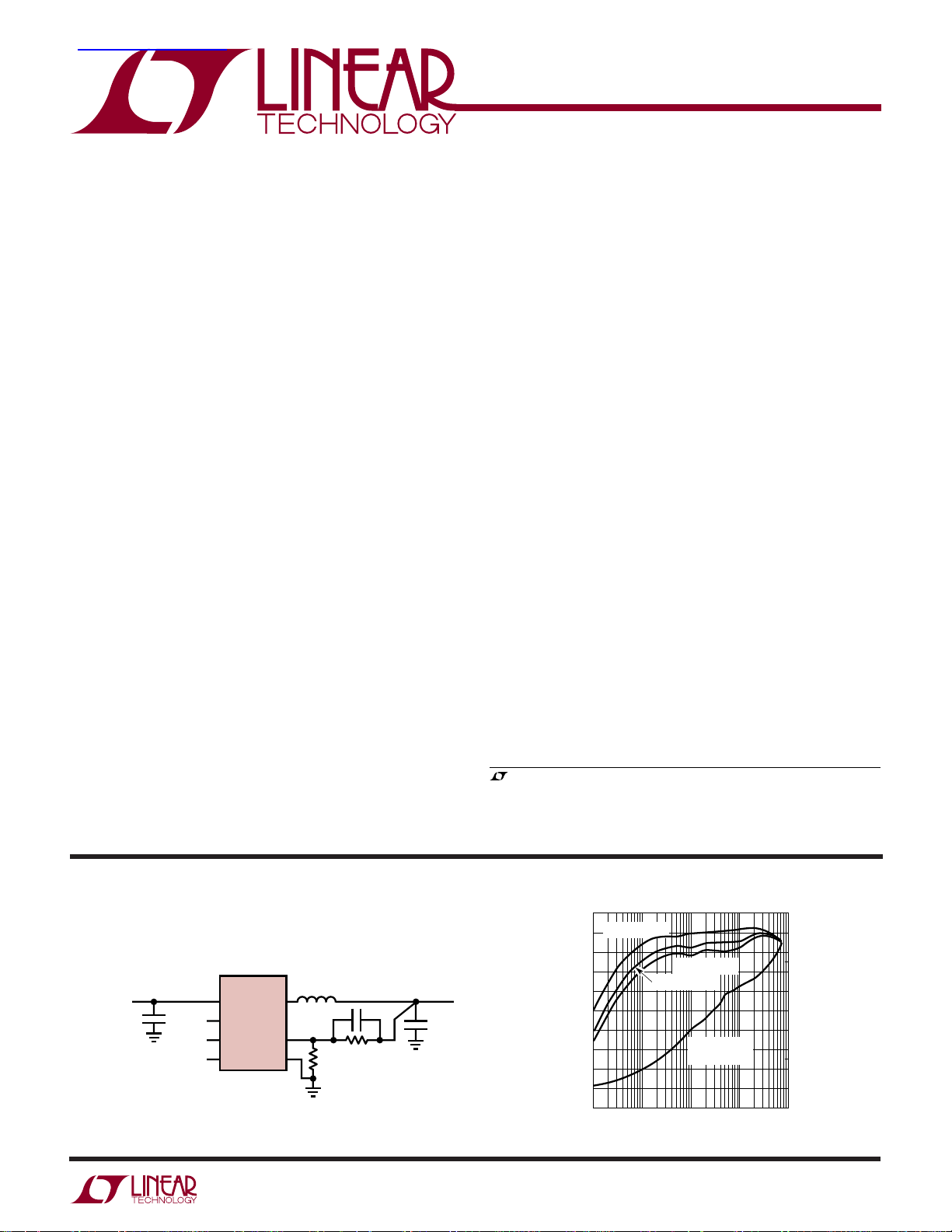
TYPICAL APPLICATIO
High Efficiency Step-Down Converter
V
1.8V TO 5.5V
IN
4.7µF
CER
*SUMIDA CDRH2D18/LD
LTC3409
V
IN
RUN
MODE
SYNC
SW
V
GND
FB
U
2.2µH*
133k
10pF
3409 TA01
255k
10µF
CER
V
1.8V
OUT
Burst Mode Efficiency, 1.8V
100
2.5VIN, BURST
90
80
70
60
50
40
EFFICIENCY (%)
30
20
10
0
0.1 10 100 1000
4.2VIN, BURST
3.6VIN, BURST
POWER LOST
3.6V
IN
1
LOAD CURRENT (mA)
, BURST
OUT
3409 TA01b
1.0
0.1
POWER LOSS (W)
0
3409f
1

LTC3409
TOP VIEW
9
DD PACKAGE
8-LEAD (3mm × 3mm) PLASTIC DFN
5
6
7
8
4
3
2
1V
FB
GND
V
IN
V
IN
SYNC
RUN
SW
MODE
ABSOLUTE AXI U RATI GS
(Note 1)
Input Supply Voltage .................................. –0.3V to 6V
RUN, VFB, MODE, SYNC Voltages . – 0.3V to (VIN + 0.3V)
SW Voltage ................................... –0.3V to (V
Operating Temperature Range (Note 2) .. –40°C to 85°C
Junction Temperature (Note 3)............................ 125°C
Storage Temperature Range ................ –65°C to 125°C
ELECTRICAL CHARACTERISTICS
The ● denotes specifications which apply over the full operating temperature range, otherwise specifications are TA = 25°C.
VIN = 2.2V unless otherwise specified.
SYMBOL PARAMETER CONDITIONS MIN TYP MAX UNITS
V
RUN
I
RUN
V
MODE
I
MODE
V
SYNCTH
I
SYNC
V
FB
I
VFB
∆V
OVL
∆V
FB
∆V
OUT
I
PK
V
LOADREG
V
IN
I
S
f
OSC
SYNC TH SYNC Threshold When SYNC Input is Toggling (Note 7) 0.63 V
SYNC f
SYNC f
SYNC PW Minimum SYNC Pulse Width 100 ns
t
SS
2
RUN Threshold ● 0.3 0.65 1.1 V
RUN Leakage Current 0.01 1 µA
MODE Threshold ● 0.3 0.65 1.1 V
MODE Leakage Current 0.01 1 µA
SYNC Threshold ● 0.3 0.65 1.1 V
SYNC Leakage Current 0.01 1 µA
Regulated Feedback Voltage (Note 4) TA = 25°C 0.6007 0.6130 0.6252 V
Feedback Current ±30 nA
∆V
Reference Voltage Line Regulation (Note 4) ● 0.04 0.4 %/V
Output Voltage Line Regulation I
Peak Inductor Current VIN = 2.2V, VFB = 0.5V or V
Output Voltage Load Regulation 0.5 %
Input Voltage Range ● 1.6 5.5 V
Input DC Bias Current (Note 5)
Active Mode V
Sleep Mode V
Shutdown V
Nominal Oscillator Frequency SYNC = GND ● 0.9 1.7 2.1 MHz
Minimum SYNC Pin Frequency 1 MHz
MIN
Maximum SYNC Pin Frequency 3 MHz
MAX
Soft-Start Period RUN↑ 1ms
WWWU
Overvoltage Lockout ∆V
FBOVL
UU
W
PACKAGE/ORDER I FOR ATIO
ORDER PART
NUMBER
+ 0.3V)
IN
T
= 125°C, θJA = 43°C/ W
JMAX
EXPOSED PAD (PIN 9) IS GND
MUST BE SOLDERED TO PCB
Consult LTC Marketing for parts specified with wider operating temperature ranges.
(Note 4) 0°C ≤ T
(Note 4) –40°C ≤ T
= ∆V
OVL
= 100mA, 1.6V < VIN < 5.5V 0.04 0.4 %/V
OUT
Duty Cycle < 35%
= 90%, I
OUT
= 103%, I
OUT
= 0V, VIN = 5.5V 0.1 5 µA
RUN
SYNC = V
≤ 85°C 0.5992 0.6130 0.6268 V
A
≤ 85°C ● 0.5977 0.6130 0.6283 V
A
– VFB (Note 6) 35 61 85 mV
FBOVL
= 90%, 0.75 1 1.3 A
OUT
= 0A 350 475 µA
LOAD
= 0A 65 120 µA
LOAD
IN
● 1.8 2.6 3.0 MHz
LTC3409EDD
DD PART MARKING
LBNM
3409f
LTC3409
ELECTRICAL CHARACTERISTICS
The ● denotes specifications which apply over the full operating temperature range, otherwise specifications are TA = 25°C.
VIN = 2.2V unless otherwise specified.
SYMBOL PARAMETER CONDITIONS MIN TYP MAX UNITS
SYNC t
R
PFET
R
NFET
I
LSW
SYNC Timeout Delay from Removal of EXT CLK Until Fixed 30 µs
O
R
of P-Channel FET ISW = 100mA, Wafer Level 0.33 Ω
DS(ON)
R
of N-Channel FET ISW = 100mA, Wafer Level 0.22 Ω
DS(ON)
SW Leakage V
Frequency Operation Begins (Note 7)
= 100mA, DD Package 0.35 Ω
I
SW
= 100mA, DD Package 0.25 Ω
I
SW
= 0V, VSW = 0V or 5V, VIN = 5V ±0.1 ±3 µA
RUN
Note 1: Absolute Maximum Ratings are those values beyond which the life
of a device may be impaired.
Note 2: The LTC3409E is guaranteed to meet performance specifications
from 0°C to 70°C. Specifications over the –40°C to 85°C operating
temperature range are assured by design, characterization and correlation
with statistical process controls.
Note 3: T
dissipation P
This IC includes overtemperature protection that is intended to protect the
device during momentary overload conditions. Overtemperature protection
becomes active at a junction temperature greater than the maximum
operating junction temperature. Continuous operation above the specified
maximum operating junction temperature may impair device reliability.
is calculated from the ambient temperature TA and power
J
according to the following formula:
D
LTC3409: TJ = TA + (PD)(43°C/W)
Note 4: The LTC3409 is tested in a proprietary test mode that connects
to the output of the error amplifier.
V
FB
Note 5: Dynamic supply current is higher due to the gate charge being
delivered at the switching frequency.
Note 6: ∆V
voltage.
Note 7: Determined by design, not production tested.
is the amount VFB must exceed the regulated feedback
OVL
3409f
3
LTC3409
UW
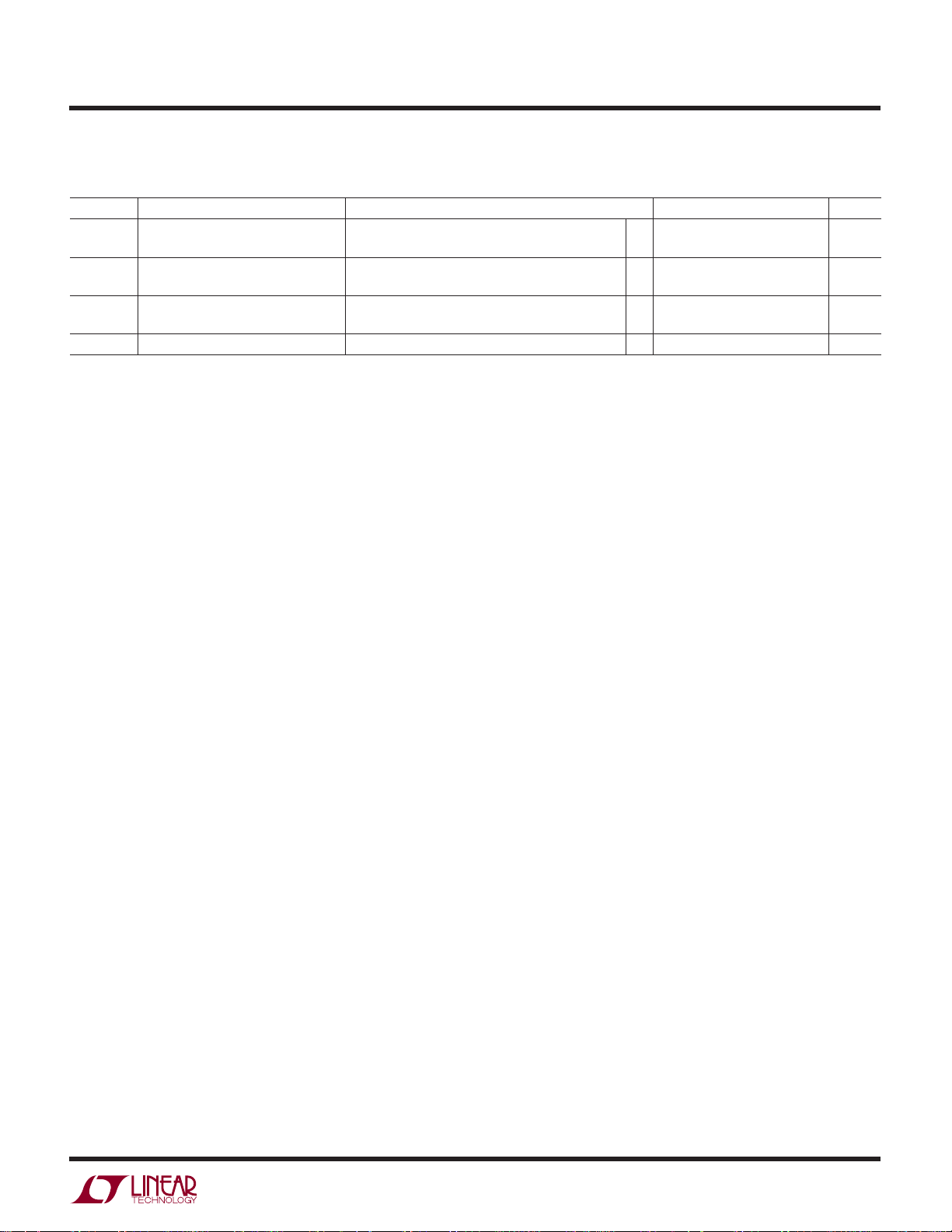
TYPICAL PERFOR A CE CHARACTERISTICS
(From Typical Application on the front page except for the resistive divider resistor values)
Efficiency/Power Lost
vs Load Current, V
100
90
80
70
60
50
40
EFFICIENCY (%)
30
20
10
0
0.1 10 100 1000
, BURST
1: 2.5V
IN
, BURST
2: 3.6V
IN
, BURST
3: 4.2V
IN
, PULSE SKIP
4: 2.5V
IN
, PULSE SKIP
5: 3.6V
IN
, PULSE SKIP
6: 4.2V
IN
1
2
3
8
10
12
1
LOAD CURRENT (mA)
7: POWER LOST, 2.5V
8: POWER LOST, 2.5V
9: POWER LOST, 3.6V
10: POWER LOST, 3.6V
11: POWER LOST, 4.2V
12: POWER LOST, 4.2V
= 1.8V
OUT
5
4
6
7
11
9
Efficiency vs Load Current
V
= 2.5V
OUT
100
BURST
90
2.7V
IN
80
70
60
50
40
EFFICIENCY (%)
30
20
10
0
0.1 10 100 1000
4.2V
IN
3.6V
IN
2.7V
IN
1
LOAD CURRENT (mA)
3.6V
4.2V
IN
PULSE SKIP
IN
1.0
0.1
0
3409 G01
, BURST
IN
, PULSE SKIP
IN
, BURST
IN
, PULSE SKIP
IN
, BURST
IN
, PULSE SKIP
IN
3409 G04
Efficiency vs Input Voltage
V
= 1.2V, Burst Mode Operation
OUT
100
90
80
POWER LOSS (mW)
70
60
50
40
EFFICIENCY (%)
30
20
10
I
= 0.1mA
OUT
I
= 1mA
OUT
= 10mA
I
OUT
0
1.5
2.5
3.5
INPUT VOLTAGE (V)
Efficiency vs Load Current
V
= 1.2V
OUT
100
BURST
1.6V
90
2.5V
IN
80
70
60
50
40
EFFICIENCY (%)
30
20
10
0
0.1 10 100 1000
IN
3.1V
IN
1.6V
IN
PULSE SKIP
1
LOAD CURRENT (mA)
3.1V
2.5V
I
I
I
IN
IN
OUT
OUT
OUT
= 100mA
= 600mA
= 800mA
4.5
3409 G05
EFFICIENCY (%)
5.5
3409 G02
0.618
0.617
0.616
0.615
0.614
0.613
0.612
0.611
REFERENCE VOLTAGE (V)
0.610
0.609
0.608
Efficiency vs Input Voltage
V
= 1.2V, Pulse Skip
OUT
100
90
80
70
60
50
40
30
20
10
0
1.5
I
= 800mA
OUT
I
OUT
I
= 1mA
OUT
I
= 0.1mA
OUT
2.5
3.5
INPUT VOLTAGE (V)
I
Reference Voltage
vs Temperature
–10–30
–50
3010
50
TEMPERATURE (°C)
I
= 600mA
OUT
= 100mA
OUT
= 10mA
4.5
70 90 130
110
5.5
3409 G03
150
1011 G06
4
3409f
LOAD CURRENT (mA)
0
1.18
OUTPUT VOLTAGE (V)
1.19
1.20
1.21
1.22
100 200 300 400
3409 G09
500 600 700 800 900
1.2V
OUT
BURST
1.2V
OUT
PULSE
SKIP
UW
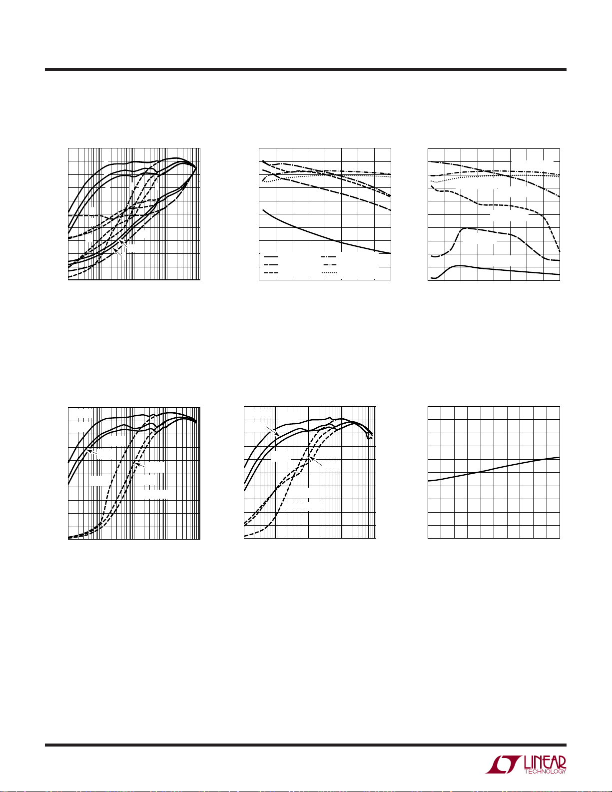
TYPICAL PERFOR A CE CHARACTERISTICS
(From Typical Application on the front page except for the resistive divider resistor values)
LTC3409
Oscillator Frequency
vs Temperature
2.70
2.60
2.50
2.40
2.30
2.20
2.10
2.00
1.90
1.80
1.70
1.60
1.50
OSCILLATOR FREQUENCY (MHz)
1.40
1.30
1.20
0.450
0.400
0.350
0.300
0.250
(Ω)
0.200
DS(0N)
R
0.150
0.100
0.050
–50
0
R
1.5
VIN = 2.7V
VIN = 4.2V
VIN = 4.2V
VIN = 1.6V
–25 0
TEMPERATURE (°C)
vs Input Voltage
DS(ON)
2.5 4.5
INPUT VOLTAGE (V)
25 75 125100
SYNCHRONOUS
3.5
VIN = 1.6V
VIN = 2.7V
50
MAIN
SWITCH
SWITCH
OSC 2.6MHz
OSC 1.7MHz
3409 G07
5.5
3409 G10
Oscillator Frequency Shift
vs Input Voltage
6
4
2
0
–2
–4
–6
OSCILLATOR FREQUENCY SHIFT (%)
–8
–10
1.5
R
DS(ON)
0.55
0.50
0.45
0.40
(Ω)
0.35
0.30
DS(ON)
R
0.25
0.20
0.15
0.10
–50
–25 0
f
LOW
1.7MHz
f
HIGH
2.6MHz
2.5
INPUT VOLTAGE (V)
vs Input Temperature
MAIN SWITCH
2.7V
SYNCHRONOUS SWITCH
25 75
TEMPERATURE (°C)
3.5
50 100 125
4.5
3409 G08
1.6V
4.2V
1.6V
2.7V
4.2V
3409 G11
5.5
Output Voltage vs Load Current
= 1.6V
V
IN
Dynamic Supply Current
vs Input Voltage
6000
5000
4000
3000
DYNAMIC SUPPLY CURRENT, PULSE SKIP (µA)
2000
1000
PULSE
0
1.5
V
OUT
I
OUT
SKIP
23
2.5
INPUT VOLTAGE (V)
BURST/SLEEP
V
= 1.5V
OUT
= 0
I
OUT
VFB = V
IN
= 1.5V
= 0
VFB = 0
5
4.5
5.5
3409 G12
46
3.5
120
100
80
60
40
20
0
DYNAMIC SUPPLY CURRENT, BURST/SLEEP (µA)
500
450
400
350
300
250
200
150
100
DYNAMIC SUPLLY CURRENT (µA)
50
0
Dynamic Supply Current vs
Temperature, VIN = 3.6V,
V
= 1.5V, 0 Load
OUT
PULSE SKIP
BURST
–50
0
–25
TEMPERATURE (°C)
50
25
75
100
3409 G13
125
Switch Leakage vs Temperature
VIN = 5.5V
6000
VIN = 5.5V
5000
4000
3000
MAIN SWITCH
2000
SWITCH LEAKAGE (nA)
1000
0
–50
SYNCHRONOUS SWITCH
–25 0
25 75
TEMPERATURE (°C)
50 100 125
3409 G14
Switch Leakage vs Input Voltage
45
40
35
30
25
20
15
SWITCH LEAKAGE (nA)
10
5
0
0
MAIN SWITCH
SYNCHRONOUS
SWITCH
2
INPUT VOLTAGE (V)
4
6
8
3409 G15
3409f
5
LTC3409
UW
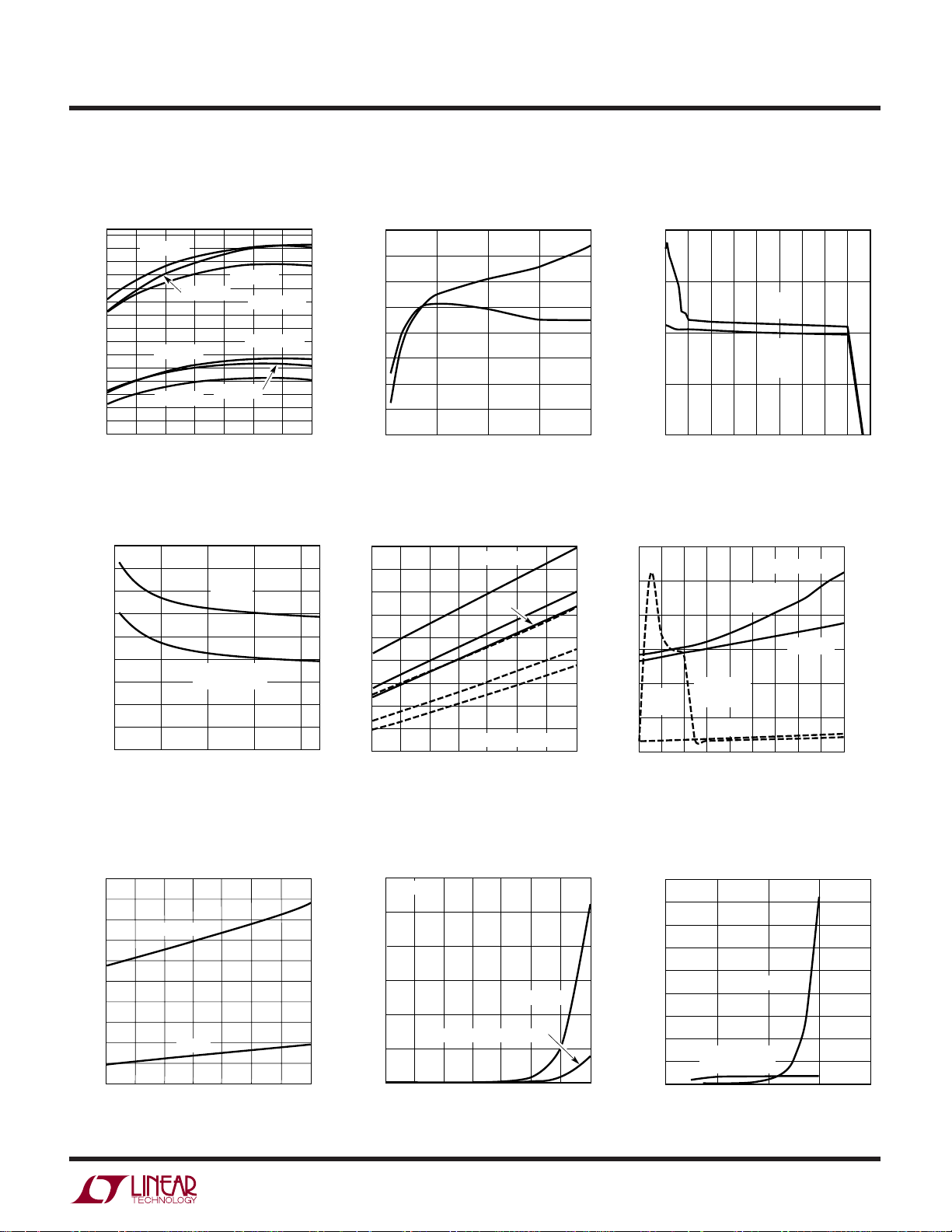
TYPICAL PERFOR A CE CHARACTERISTICS
(From Typical Application on the front page except for the resistive divider resistor values)
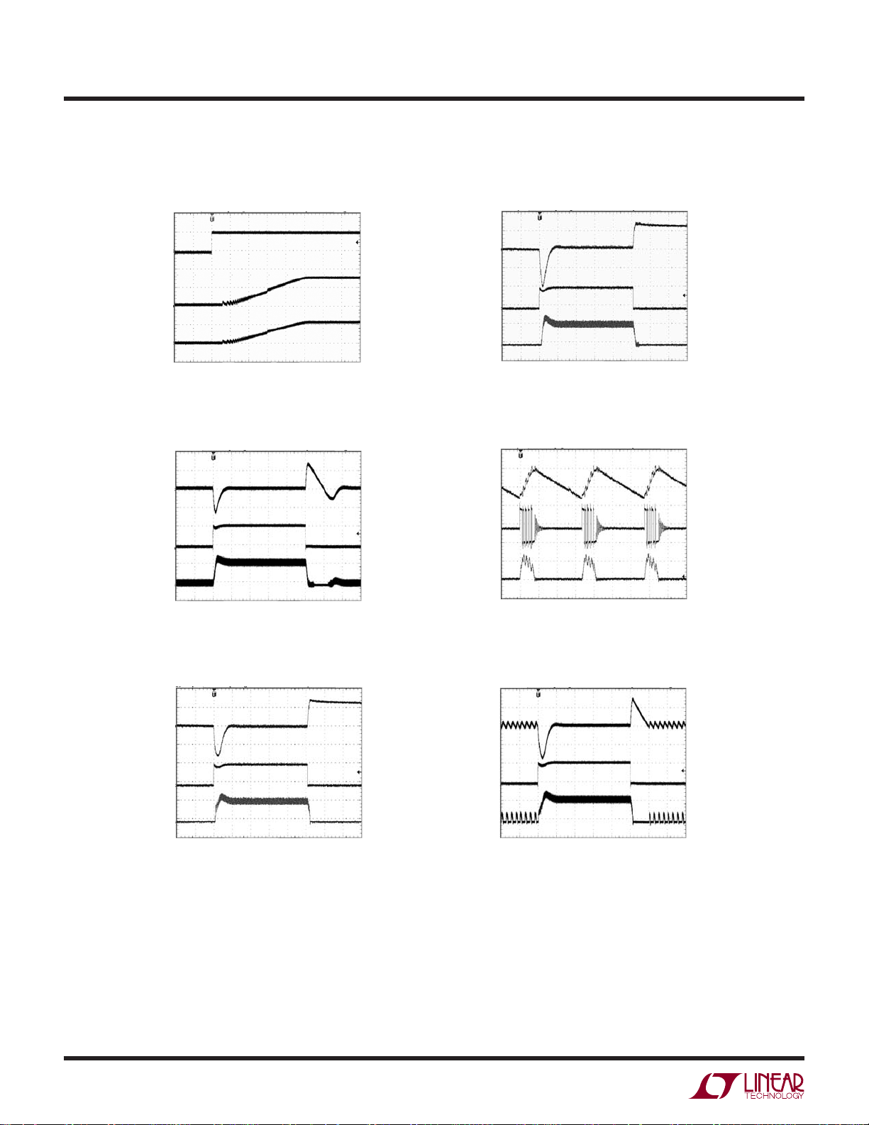
Load Step 0mA to 600mA
Start-Up from Shutdown
Pulse Skip
RUN
2V/DIV
V
OUT
1V/DIV
INDUCTOR
CURRENT
500mA/DIV
V
OUT
100mV/DIV
I
LOAD
500mA/DIV
INDUCTOR
CURRENT
500mA/DIV
200µs/DIV
Load Step 50mA to 600mA
Pulse Skip
20µs/DIV
3409 G16
3409 G18
V
OUT
100mV/DIV
I
LOAD
500mA/DIV
INDUCTOR
CURRENT
500mA/DIV
V
OUT
20mV/DIV
V
SWITCH
2V/DIV
INDUCTOR
CURRENT
200mA/DIV
20µs/DIV
Burst Mode Operation
I
= 35mA
LOAD
2µs/DIV
3409 G17
3409 G19
V
OUT
100mV/DIV
I
LOAD
500mA/DIV
INDUCTOR
CURRENT
500mA/DIV
Load Step 0mA to 600mA
Burst Mode Operation
20µs/DIV
3409 G20
V
OUT
100mV/DIV
I
LOAD
500mA/DIV
INDUCTOR
CURRENT
500mA/DIV
Load Step 50mA to 600mA
Burst Mode Operation
20µs/DIV
3409 G21
3409f
6

LTC3409
U
UU
PI FU CTIO S
VFB (Pin 1): Feedback Pin. Receives the feedback voltage
from an external resistive divider across the output.
GND (Pin 2): Ground Pin.
VIN (Pins 3, 4): Main Supply Pins. Must be closely
decoupled to GND, Pin 2 and Pin 9, with a 4.7µF or greater
ceramic capacitor.
MODE (Pin 5): Mode Select Input. To select pulse skipping
mode, force this pin above 1.1V. Forcing this pin below
0.3V selects Burst Mode operation. Do not leave MODE
floating.
SW (Pin 6): Switch Node Connection to Inductor. This pin
connects to the drains of the internal main and synchronous power MOSFET switches.
RUN (Pin 7): Run Control Input. Forcing this pin above
1.1V enables the part. Forcing this pin below 0.3V shuts
down the device. In shutdown, all functions are disabled
drawing <1µA supply current. Do not leave RUN floating.
SYNC (Pin 8): External CLK Input/Fixed Switching Frequency Selection. Forcing this pin above 1.1V for greater
than 30µs selects 2.6MHz switching frequency. Forcing
this pin below 0.3V for greater than 30µs selects 1.7MHz
switching frequency.
External clock input, 1MHz to 3MHz frequency range.
When the SYNC pin is clocked in this frequency range the
SYNC threshold is nominally 0.63V. To allow for good
noise immunity, SYNC signal should swing at least 0.3V
below and above this nominal value (0.33V to 0.93V). Do
not leave SYNC floating.
GND (Pin 9): Exposed Pad. The Exposed Pad is ground. It
must be soldered to PCB ground to provide both electrical
contact and optimum thermal performance.
3409f
7

LTC3409
U
U
W
FU CTIO AL DIAGRA
MODE
5
+
–
EA
+
OVDET
–
SLOPE
COMP
SYNC
8
V
FB
1
RUN
7
V
IN
REFERENCE
SHUTDOWN
PLL
0.613V
SOFTSTART
0.675
OV
0.65V
OSC
V
–
+
0.4V
EN
–
+
BURST
Q
S
R
Q
RS LATCH
SLEEP
SWITCHING
LOGIC
AND
BLANKING
CIRCUIT
–
I
COMP
ANTI-
SHOOT-
THRU
I
RCMP
+
+
–
5Ω
3, 4
3409 FD
IN
SW
6
GND
2
U
OPERATIO
Main Control Loop
The LTC3409 uses a constant frequency, current mode
step-down architecture. Both the main (P-channel
MOSFET) and synchronous (N-channel MOSFET) switches
are internal. During normal operation, the internal top
power MOSFET is turned on each cycle when the oscillator
sets the RS latch, and turned off when the current comparator, I
current at which I
the output of error amplifier EA. The VFB pin, described in
the Pin Functions section, allows EA to receive an output
feedback voltage from an external resistive divider. When
the load current increases, it causes a slight decrease in
the feedback voltage relative to the 0.613V reference,
which in turn, causes the EA amplifier’s output voltage to
increase until the average inductor current matches the
new load current. While the top MOSFET is off, the bottom
MOSFET is turned on until either the inductor current
, resets the RS latch. The peak inductor
COMP
resets the RS latch is controlled by
COMP
starts to reverse, as indicated by the current reversal
comparator I
, or the beginning of the next clock
RCMP
cycle.
Comparator OVDET guards against transient overshoots
>10% by turning the main switch off and keeping it off until
the transient has ended.
Burst Mode Operation
The LTC3409 is capable of Burst Mode operation in which
the internal power MOSFETs operate intermittently based
on load demand. To enable Burst Mode operation, simply
connect the MODE pin to GND. To disable Burst Mode
operation and enable PWM pulse skipping mode, connect
the MODE pin to VIN or drive it with a logic high (V
MODE
>1.1V). In this mode, the efficiency is lower at light loads,
but becomes comparable to Burst Mode operation when
the output load exceeds 30mA. The advantage of pulse
8
3409f

OPERATIO
LTC3409
U
skipping mode is lower output ripple and less interference
to audio circuitry. When the converter is in Burst Mode
operation, the minimum peak current of the inductor is set
to approximately 200mA regardless of the output load.
Each burst event can last from a few cycles at light loads
to almost continuously cycling with short sleep intervals
at moderate loads. In between these burst events, the
power MOSFETs and any unneeded circuitry are turned
off, reducing the quiescent current to 65µA. In this sleep
state, the load current is being supplied solely from the
output capacitor. As the output voltage droops, the EA
amplifier’s output rises above the sleep threshold signaling the BURST comparator to trip and turn the top MOSFET
on. This process repeats at a rate that is dependent on the
load demand.
Short-Circuit Protection
When the output is shorted to ground the LTC3409 limits
the synchronous switch current to 1.5A. If this limit is
exceeded, the top power MOSFET is inhibited from turning on until the current in the synchronous switch falls
below 1.5A.
Dropout Operation
As the input supply voltage decreases to a value approaching the output voltage, the duty cycle increases
toward the maximum on-time. Further reduction of the
supply voltage forces the main switch to remain on for
more than one cycle.
Slope Compensation
Slope compensation provides stability in constant frequency architectures by preventing subharmonic oscillations at high duty cycles. It is accomplished internally by
adding a compensating ramp to the inductor current
signal at duty cycles in excess of 40%.
User Controlled Switching Frequency
The internal oscillator of the LTC3409 can be synchronized
to a user-supplied external clock applied to the SYNC pin.
Alternately, when this pin is held at a fixed High or Low
level for more than 30µs, the internal oscillator will revert
to fixed-frequency operation; where the frequency may be
selected as 1.7MHz (SYNC Low) or 2.6MHz (SYNC High).
Internal Soft-Start
At start-up when the RUN pin is brought high, the internal
reference is linearly ramped from 0V to 0.613V in 1ms. The
regulated feedback voltage will follow this ramp resulting
in the output voltage ramping from 0% to 100% in 1ms.
The current in the inductor during soft-start will be defined
by the combination of the current needed to charge the
output capacitance and the current provided to the load as
the output voltage ramps up. The start-up waveform,
shown in the Typical Performance Characteristics, shows
the output voltage start-up from 0V to 1.5V with a 2.5Ω
load and VIN = 2.2V. The 2.5Ω load results in an output of
600mA at 1.5V.
3409f
9

LTC3409
WUUU
APPLICATIO S I FOR ATIO
The basic LTC3409 application circuit is shown on the first
page of this data sheet. External component selection is
driven by the load requirement and begins with the selection of L followed by CIN and C
OUT
.
Inductor Selection
For most applications, the value of the inductor will fall in
the range of 1µH to 10µH. Its value is chosen based on the
desired ripple current. Large value inductors lower ripple
current and small value inductors result in higher ripple
currents. Higher VIN or V
also increases the ripple
OUT
current as shown in Equation 1. A reasonable starting
point for setting ripple current is ∆IL = 240mA (40% of
600mA).
∆ =
1
I
L OUT
fL
⎛
1•–
V
⎜
⎝
V
OUT
V
IN
⎞
⎟
⎠
(1)
The DC current rating of the inductor should be at least
equal to the maximum load current plus half the ripple
current to prevent core saturation. Thus, a 720mA rated
inductor should be enough for most applications (600mA
+ 120mA). For better efficiency, choose a low DC resistance inductor. The inductor value also has an effect on
Burst Mode operation. The transition to low current operation begins when the inductor current peaks fall to approximately 200mA. Lower inductor values (higher ∆IL)
will cause this to occur at lower load currents, which can
cause a dip in efficiency in the upper range of low current
operation. In Burst Mode operation, lower inductance
values will cause the burst frequency to increase.
Inductor Core Selection
Different core materials and shapes will change the size/
current and price/current relationship of an inductor.
Toroid or shielded pot cores in ferrite or permalloy materials are small and don’t radiate much energy, but generally cost more than powdered iron core inductors with
similar electrical characteristics. The choice of which style
inductor to use often depends more on the price vs size
requirements and any radiated field/EMI requirements
than on what the LTC3409 requires to operate. Table 1
shows some typical surface mount inductors that work
well in LTC3409 applications.
Table 1. Representative Surface Mount Inductors
PART VALUE DCR MAX DC SIZE
NUMBER (µH) (Ω MAX) CURRENT (A) W × L × H (mm
Sumida 2.2 0.041 0.85 3.2 × 3.2 × 2.0
CDRH3D18/LD 3.3 0.054 0.75
Sumida 1.5 0.068 0.90 3.2 × 3.2 × 1.2
CDRH2D11 2.2 0.170 0.78
Sumida 2.2 0.116 0.950 4.4 × 5.8 × 1.2
CMD4D11 3.3 0.174 0.770
Murata 1.0 0.060 1.00 2.5 × 3.2 × 2.0
LQH32CN 2.2 0.097 0.79
Toko 2.2 0.060 1.08 2.5 × 3.2 × 2.0
D312F 3.3 0.260 0.92
Panasonic 3.3 0.17 1.00 4.5 × 5.4 × 1.2
ELT5KT 4.7 0.20 0.95
CIN and C
Selection
OUT
3
)
In continuous mode, the source current of the top MOSFET is a square wave of duty cycle V
OUT/VIN
. To prevent
large voltage transients, a low ESR input capacitor sized
for the maximum RMS current must be used. The maximum RMS capacitor current is given by:
12
VVV
[]
C quired I I
Re
IN RMS OUT MAX
≅
()
OUT IN OUT
This formula has a maximum at VIN = 2V
= I
/2. This simple worst-case condition is commonly
OUT
–
()
V
IN
, where I
OUT
/
RMS
used for design because even significant deviations do not
offer much relief. Note that the capacitor manufacturer’s
ripple current ratings are often based on 2000 hours of life.
This makes it advisable to further derate the capacitor, or
choose a capacitor rated at a higher temperature than
required. Always consult the manufacturer if there is any
question. The selection of C
is driven by the required
OUT
effective series resistance (ESR). Typically, once the ESR
requirement for C
rating generally far exceeds the I
The output ripple DV
∆ = ∆ +
V I ESR
OUT L
has been met, the RMS current
OUT
RIPPLE(P-P)
is determined by:
OUT
⎛
⎜
⎝
8• •
fC
⎞
1
⎟
⎠
OUT
requirement.
10
3409f

VV
R
R
OUT
=+
⎛
⎝
⎜
⎞
⎠
⎟
0 613 1
1
2
.
WUUU
V
FB
V
OUT
R1
R2
3409 F01
GND
LTC3409
APPLICATIO S I FOR ATIO
LTC3409
where f = operating frequency, C
= output capacitance
OUT
and ∆IL = ripple current in the inductor. For a fixed output
voltage, the output ripple is highest at maximum input
voltage since ∆IL increases with input voltage. Aluminum
electrolytic and dry tantalum capacitors are both available
in surface mount configurations. In the case of tantalum,
it is critical that the capacitors are surge tested for use in
switching power supplies. An excellent choice is the AVX
TPS series of surface mount tantalum. These are specially
constructed and tested for low ESR so they give the lowest
ESR for a given volume. Other capacitor types include
Sanyo POSCAP, Kemet T510 and T495 series, and Sprague
593D and 595D series. Consult the manufacturer for other
specific recommendations.
Using Ceramic Input and Output Capacitors
Higher value, lower cost ceramic capacitors are now
available in smaller case sizes. Their high ripple current,
high voltage rating and low ESR make them ideal for
switching regulator applications. Because the LTC3409’s
control loop does not depend on the output capacitor’s
ESR for stable operation, ceramic capacitors can be used
to achieve very low output ripple and small circuit size.
However, care must be taken when these capacitors are
used at the input and the output. When a ceramic capacitor
is used at the input and the power is supplied by a wall
adapter through long wires, a load step at the output can
induce ringing at the input, VIN. At best, this ringing can
couple to the output and be mistaken as loop instability. At
worst, a sudden inrush of current through the long wires
can potentially cause a voltage spike at VIN, large enough
to damage the part.
When choosing the input and output ceramic capacitors,
choose the X5R or X7R dielectric formulations. These
dielectrics have the best temperature and voltage characteristics of all the ceramics for a given value and size.
Output Voltage Programming
The output voltage is set by a resistive divider according
to the following formula:
The external resistive divider is connected to the output,
allowing remote voltage sensing as shown in Figure 1.
Figure 1
Efficiency Considerations
The efficiency of a switching regulator is equal to the
output power divided by the input power times 100%. It is
often useful to analyze individual losses to determine what
is limiting the efficiency and which change would produce
the most improvement. Efficiency can be expressed as:
Efficiency = 100% – (L1 + L2 + L3 + ...)
where L1, L2, etc. are the individual losses as a percentage
of input power.
Although all dissipative elements in the circuit produce
losses, two main sources usually account for most of the
losses in LTC3409 circuits: V
quiescent current and I2R
IN
losses. The VIN quiescent current loss dominates the
efficiency loss at very low load currents whereas the I2R
loss dominates the efficiency loss at medium to high load
currents. In a typical efficiency plot, the efficiency curve at
very low load currents can be misleading since the actual
power lost is of no consequence as illustrated in Figure 2.
3409f
11

LTC3409
WUUU
APPLICATIO S I FOR ATIO
1
BURST
PULSE SKIP
0.1
2.5V
0.01
POWER LOSS (W)
0.001
0.0001
IN
3.6V
IN
4.2V
IN
4.2V
IN
0.1 10 100 1000
3.6V
IN
2.5V
IN
1
LOAD CURRENT (mA)
Figure 2
3409 F02
1. The VIN quiescent current is due to two components: the
DC bias current as given in the Electrical Characteristics
and the internal main switch and synchronous switch
gate charge currents. The gate charge current results
from switching the gate capacitance of the internal power
MOSFET switches. Each time the gate is switched from
high to low to high again, a packet of charge, dQ, moves
from VIN to ground. The resulting dQ/dt is the current
out of VIN that is typically larger than the DC bias current. In continuous mode, I
GATECHG
= (QT + QB) where
QT and QB are the gate charges of the internal top and
bottom switches. Both the DC bias and gate charge losses
are proportional to VIN and thus their effects will be more
pronounced at higher supply voltages.
2. I2R losses are calculated from the resistances of the
internal switches, RSW, and external inductor RL. In
continuous mode, the average output current flowing
through inductor L is “chopped” between the main
switch and the synchronous switch. Thus, the series
resistance looking into the SW pin is a function of both
top and bottom MOSFET R
DS(ON)
and the duty cycle
(DC) as follows:
RSW = (R
The R
DS(ON)TOP
for both the top and bottom MOSFETs can
DS(ON)
)(DC) + (R
DS(ON)BOT
)(1 – DC)
be obtained from the Typical Performance Characteristics. Thus, to obtain I2R losses, simply add RSW to R
L
and multiply the result by the square of the average
output current.
Other losses including CIN and C
ESR dissipative
OUT
losses and inductor core losses generally account for less
than 2% total additional loss.
Thermal Considerations
In most applications the LTC3409 does not dissipate
much heat due to its high efficiency. But, in applications
where the LTC3409 is running at high ambient temperature with low supply voltage and high duty cycles, such as
in dropout, the heat dissipated may exceed the maximum
junction temperature of the part. If the junction temperature reaches approximately 150°C, both power switches
will be turned off and the SW node will become high
impedance.
To avoid the LTC3409 from exceeding the maximum
junction temperature, the user will need to do a thermal
analysis. The goal of the thermal analysis is to determine
whether the operating conditions exceed the maximum
junction temperature of the part. The temperature rise is
given by:
TR = (PD)(θJA)
where PD is the power dissipated by the regulator and θ
JA
is the thermal resistance from the junction of the die to the
ambient temperature.
The junction temperature, TJ, is given by:
TJ = TA + T
R
where TA is the ambient temperature.
As an example, consider the LTC3409 in dropout at an
input voltage of 1.6V, a load current of 600mA and an
ambient temperature of 75°C. From the typical performance graph of switch resistance, the R
DS(ON)
of the
P-channel switch at 75°C is approximately 0.48Ω. Therefore, power dissipated by the part is:
LOAD
2
• R
DS(ON)
= 172.8mW
PD = I
For the DD8 package, the θJA is 43°C/W. Thus, the junction
temperature of the regulator is:
TJ = 75°C + (0.1728)(43) = 82.4°C
which is well below the maximum junction temperature of
125°C.
12
3409f

WUUU
APPLICATIO S I FOR ATIO
LTC3409
Note that at higher supply voltages, the junction temperature is lower due to reduced switch resistance (R
DS(ON)
).
Checking Transient Response
The regulator loop response can be checked by looking at
the load transient response. Switching regulators take
several cycles to respond to a step in load current. When
a load step occurs, V
equal to (∆I
resistance of C
discharge C
• ESR), where ESR is the effective series
LOAD
OUT
, which generates a feedback error signal.
OUT
The regulator loop then acts to return V
state value. During this recovery time V
immediately shifts by an amount
OUT
. ∆I
also begins to charge or
LOAD
to its steady
OUT
can be moni-
OUT
tored for overshoot or ringing that would indicate a stability problem. For a detailed explanation of switching control
loop theory, see Application Note 76.
A second, more severe transient is caused by switching in
loads with large (>1µF) supply bypass capacitors. The
discharged bypass capacitors are effectively put in parallel
with C
, causing a rapid drop in V
OUT
. No regulator can
OUT
deliver enough current to prevent this problem if the load
switch resistance is low and it is driven quickly. The only
solution is to limit the rise time of the switch drive so that
the load rise time is limited to approximately (25 • C
LOAD
).
Thus, a 10µF capacitor charging to 3.3V would require a
250µs rise time, limiting the charging current to about
130mA.
Board Layout Considerations
When laying out the printed circuit board, the following
checklist should be used to ensure proper operation of the
LTC3409. These items are also illustrated graphically in
the layout diagram of Figure 3. Check the following in your
layout.
1. Does the capacitor CIN connect to the power V
IN
(Pins 3, 4) and GND (Exposed Pad) as close as possible? This capacitor provides the AC current to the
internal power MOSFETs and their drivers.
2. Are the C
C
returns current to GND and the (–) plate of CIN.
OUT
and L1 closely connected? The (–) plate of
OUT
3. The resistor divider, R1 and R2, must be connected
between the (+) plate of C
and a ground sense line
OUT
terminated near GND (Exposed Pad). The feedback
signals V
should be routed away from noisy compo-
FB
nents and traces, such as the SW line (Pins 6), and its
trace should be minimized.
4. Keep sensitive components away from the SW pins.
The input capacitor C
and the resistors R1 and R2
IN
should be routed away from the SW traces and the
inductors.
5. A ground plane is preferred, but if not available, keep the
signal and power grounds segregated with small signal
components returning to the GND pin at one point. They
should not share the high current path of CIN or C
OUT
.
6. Flood all unused areas on all layers with copper. Flooding with copper will reduce the temperature rise of
power components. These copper areas should be
connected to VIN or GND.
V
IN
C
IN
V
V
IN
IN
LTC3409
SYNC
RUN
MODE
V
FB
SW
SGND GND
R2
Figure 3
L1
C1
R1
3409 F03
V
OUT
C
OUT
3409f
13

LTC3409
LOAD CURRENT (mA)
30
EFFICIENCY (%)
90
100
20
10
80
50
70
60
40
0.1 10 100 1000
3409 F04b
0
1
1.8V
IN
3.2V
IN
2.5V
IN
WUUU
APPLICATIO S I FOR ATIO
Design Example
As a design example, assume the LTC3409 is used in a
2-alkaline cell battery-powered application. The V
will be
IN
operating from a maximum of 3.2V down to about 1.8V.
The load current requirement is a maximum of 600mA but
most of the time it will be in standby mode, requiring only
2mA. Efficiency at both low and high load currents is
important. Output voltage is 1.5V. With this information
we can calculate L using Equation 2:
=
fI
1
∆
L
L
Substituting V
⎛
V
1•–
⎜
OUT
⎝
= 1.5V, VIN = 3.2V, ∆IL = 240mA and
OUT
V
OUT
V
IN
⎞
⎟
⎠
(2)
f = 1.7MHz in Equation 2 gives:
L
V
1.6V TO 5.5V
1
MHz mA
1 7 240
.•
IN
C
IN
4.7µF
R2
133k
15 1
15
.
⎛
.–
⎜
⎝
32
.
LTC3409
V
FB
GND
V
IN
V
IN
R1
191k
C1
10pF
⎞
≅ µ
⎟
⎠
SYNC
RUN
SW
MODE
L1: SUMIDA CDRH2D18/LD
22
.
H=
L1
2.2µH
3409 F04
For best efficiency choose a 750mA or greater inductor
with less than 0.3Ω series resistance. CIN will require an
RMS current rating of at least 0.3A ≅ I
LOAD(MAX)
/2 at
temperature.
For the feedback resistors, choose R2 = 133k. R1 can then
be calculated from Equation 2 at 191K. Figure 4 shows the
complete circuit along with its efficiency curve.
Table 2 below gives 1% resistor values for selected output
voltages.
V
OUT
0.85V 51.1k 133k
1.2V 127k 133k
1.5V 191k 133k
1.8V 255k 133k
V
OUT
1.5V
C
0.6A
OUT
10µF
CER
R1 R2
Burst Mode Efficiency, 1.5V
OUT
14
Figure 4
3409f

PACKAGE DESCRIPTIO
LTC3409
U
DD Package
8-Lead Plastic DFN (3mm × 3mm)
(Reference LTC DWG # 05-08-1698)
0.675 ±0.05
3.5 ±0.05
1.65 ±0.05
(2 SIDES)2.15 ±0.05
PACKAGE
OUTLINE
0.25 ± 0.05
RECOMMENDED SOLDER PAD PITCH AND DIMENSIONS
PIN 1
TOP MARK
(NOTE 6)
0.200 REF
NOTE:
1. DRAWING TO BE MADE A JEDEC PACKAGE OUTLINE M0-229 VARIATION OF (WEED-1)
2. DRAWING NOT TO SCALE
3. ALL DIMENSIONS ARE IN MILLIMETERS
4. DIMENSIONS OF EXPOSED PAD ON BOTTOM OF PACKAGE DO NOT INCLUDE
MOLD FLASH. MOLD FLASH, IF PRESENT, SHALL NOT EXCEED 0.15mm ON ANY SIDE
5. EXPOSED PAD SHALL BE SOLDER PLATED
6. SHADED AREA IS ONLY A REFERENCE FOR PIN 1 LOCATION
ON TOP AND BOTTOM OF PACKAGE
0.50
BSC
2.38 ±0.05
(2 SIDES)
3.00 ±0.10
(4 SIDES)
0.75 ±0.05
0.00 – 0.05
1.65 ± 0.10
(2 SIDES)
R = 0.115
TYP
0.25 ± 0.05
2.38 ±0.10
(2 SIDES)
BOTTOM VIEW—EXPOSED PAD
0.38 ± 0.10
85
14
0.50 BSC
(DD8) DFN 1203
Information furnished by Linear Technology Corporation is believed to be accurate and reliable.
However, no responsibility is assumed for its use. Linear Technology Corporation makes no representation that the interconnection of its circuits as described herein will not infringe on existing patent rights.
3409f
15
LTC3409
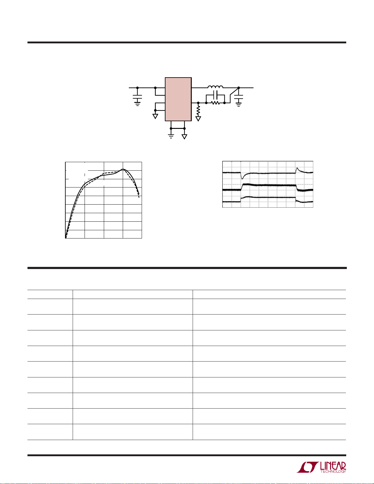
TYPICAL APPLICATIO
2-Cell to 1.2V/600mA Regulator for High Efficiency and Low Profile
U
95
VIN = 1.8V
= 1.2V
V
90
OUT
f = 1.7MHz
85
80
75
70
EFFICIENCY (%)
65
60
55
50
0.0001
V
1.8V TO 3V
LTC3409
IN
C
IN
4.7µF
CER
3, 4
7
5
8
V
IN
RUN
MODE
V
SYNC
GND SGND
92
SW
FB
3409 TA02a
2.2µH*
6
22pF
1
287k
301k
: TDK C1608X5R0J475M
C
IN
: TDK C1608X5R0G106M
C
OUT
*SUMIDA CDRH2D09NP-2R2NC
C
OUT
10µF
CER
V
Efficiency Load Step
V
OUT
100mV/DIV
f = 2.6MHz
0.001
0.01
OUTPUT CURRENT (mA)
0.1
1
3409 TA02b
AC COUPLED
500mA/DIV
I
LOAD
500mA/DIV
I
L
= 1.8V
V
IN
= 1.2V
V
OUT
= 200mA TO 600mA
I
LOAD
OUT
1.2V
20µs/DIV
3409 TA02c
RELATED PARTS
PART NUMBER DESCRIPTION COMMENTS
LTC1878 600mA (I
DC/DC Converter I
LTC1879 1.20A (I
DC/DC Converter I
LT3020 100mA, Low Voltage VLDO
LTC3025 100mA, Low Voltage VLDO VIN: 0.9V to 5.5V, V
LTC3404 600mA (I
DC/DC Converter I
LTC3405/LTC3405A 300mA (I
DC/DC Converter I
LTC3406/LTC3406B 600mA (I
DC/DC Converter I
LTC3407 Dual, 600mA (I
DC/DC Converter I
LTC3411 1.25A (I
DC/DC Converter I
VLDO and ThinSOT are trademarks of Linear Technology Corporation.
Linear Technology Corporation
16
1630 McCarthy Blvd., Milpitas, CA 95035-7417
(408) 432-1900 ● FAX: (408) 434-0507
), 550kHz, Synchronous Step-Down 96% Efficiency, VIN: 2.7V to 6V, V
OUT
), 550kHz, Synchronous Step-Down 95% Efficiency, VIN: 2.7V to 10V, V
OUT
TM
), 1.4MHz, Synchronous Step-Down 96% Efficiency, VIN: 2.7V to 6V, V
OUT
), 1.5MHz, Synchronous Step-Down 95% Efficiency, VIN: 2.5V to 5.5V, V
OUT
), 1.5MHz, Synchronous Step-Down 96% Efficiency, VIN: 2.5V to 5.5V, V
OUT
), 1.5MHz, Synchronous Step-Down 95% Efficiency, VIN: 2.5V to 5.5V, V
OUT
), 4MHz, Synchronous Step-Down 95% Efficiency, VIN: 2.5V to 5.5V, V
OUT
●
www.linear.com
< 1µA, MS8 Package
SD
< 1µA, 16-Lead TSSOP
SD
VIN: 0.9V to 10V, V
I
= 120µA, ISD < 3µA, V
Q
= 54µA, ISD < 1µA, V
I
Q
< 1µA, MS8 Package
SD
< 1µA, ThinSOTTM Package
SD
< 1µA, ThinSOT Package
SD
< 1µA, 10-Lead MSE Package
SD
< 1µA, 10-Lead MS Package
SD
= 0.8V, IQ = 10µA,
OUT(MIN)
= 0.8V, IQ = 15µA,
OUT(MIN)
= 0.20V, Dropout Voltage = 0.15V,
OUT(MIN)
= ADJ, DFN/MS8 Packages
OUT
= 0.40V, Dropout Voltage = 0.05V,
OUT(MIN)
= ADJ, DFN Package
OUT
= 0.8V, IQ = 10µA,
OUT(MIN)
= 0.8V, IQ = 20µA,
OUT(MIN)
= 0.6V, IQ = 20µA,
OUT(MIN)
= 0.6V, IQ = 40µA,
OUT(MIN)
= 0.8V, IQ = 60µA,
OUT(MIN)
LT/TP 0205 1K • PRINTED IN THE USA
© LINEAR TECHNOLOGY CORPORATION 2005
3409f
 Loading...