

查询LT3014HVES5供应商
FEATURES
■
VIN Range: 0.9V to 10V
■
Minimum Input Voltage: 0.9V
■
Dropout Voltage: 150mV Typical
■
Output Current: 100mA
■
Adjustable Output (V
■
Fixed Output Voltages: 1.2V, 1.5V, 1.8V
■
Stable with Low ESR, Ceramic Output Capacitors
REF
= V
OUT(MIN)
= 200mV)
(2.2µF Minimum)
■
0.2% Load Regulation from 1mA to 100mA
■
Quiescent Current: 120µA (Typ)
■
3µA Typical Quiescent Current in Shutdown
■
Current Limit Protection
■
Reverse-Battery Protection
■
No Reverse Current
■
Thermal Limiting with Hysteresis
■
8-Lead DFN (3mm × 3mm) and MSOP Packages
U
APPLICATIO S
■
Low Current Regulators
■
Battery-Powered Systems
■
Cellular Phones
■
Pagers
■
Wireless Modems
LT3020/LT3020-1.2/
LT3020-1.5/LT3020-1.8
100mA, Low Voltage,
Very Low Dropout
Linear Regulator
U
DESCRIPTIO
The LT®3020 is a very low dropout voltage (VLDOTM) linear
regulator that operates from input supplies down to 0.9V.
This device supplies 100mA of output current with a
typical dropout voltage of 150mV. The LT3020 is ideal for
low input voltage to low output voltage applications,
providing comparable electrical efficiency to that of a
switching regulator.
The LT3020 regulator optimizes stability and transient
response with low ESR, ceramic output capacitors as
small as 2.2µF. Other LT3020 features include 0% typical
line regulation and 0.2% typical load regulation. In shutdown, quiescent current drops to 3µA.
Internal protection circuitry includes reverse-battery protection, current limiting, thermal limiting with hysteresis,
and reverse-current protection. The LT3020 is available as
an adjustable output device with an output range down to
the 200mV reference. Three fixed output voltages, 1.2V,
1.5V and 1.8V, are also available.
The LT3020 regulator is available in the low profile
(0.75mm) 8-lead (3mm × 3mm) DFN package with Exposed Pad and the 8-lead MSOP package.
, LTC and LT are registered trademarks of Linear Technology Corporation.
VLDO is a trademark of Linear Technology Corporation.
All other trademarks are the property of their respective owners.
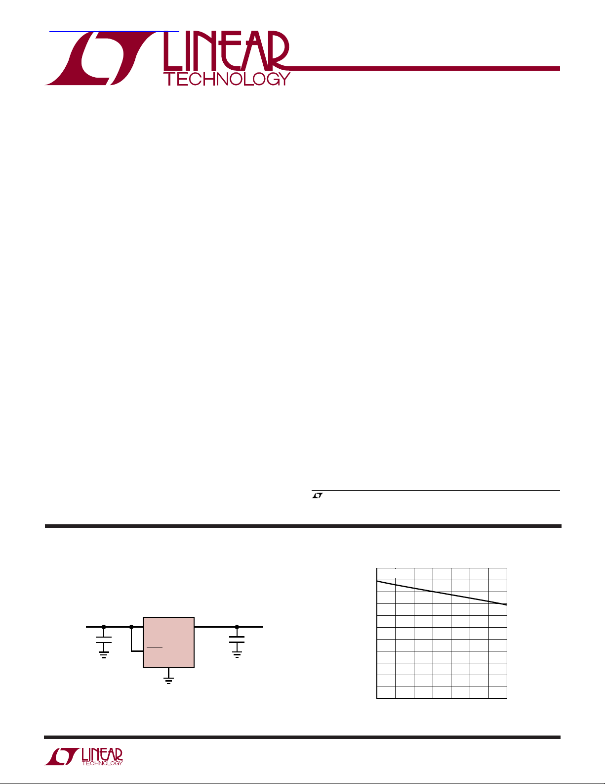
TYPICAL APPLICATIO
1.8V to 1.5V, 100mA VLDO Regulator
V
1.8V
IN
2.2µF
IN
LT3020-1.5
SHDN
OUT
GND
U
3020 TA01
2.2µF
V
OUT
1.5V
100mA
Minimum Input Voltage
1.1
IL = 100mA
1.0
0.9
0.8
0.7
0.6
0.5
0.4
0.3
MINIMUM INPUT VOLTAGE (V)
0.2
0.1
0
–50
250–25 50 75
TEMPERATURE (°C)
125100
3020 TA02
3020fc
1
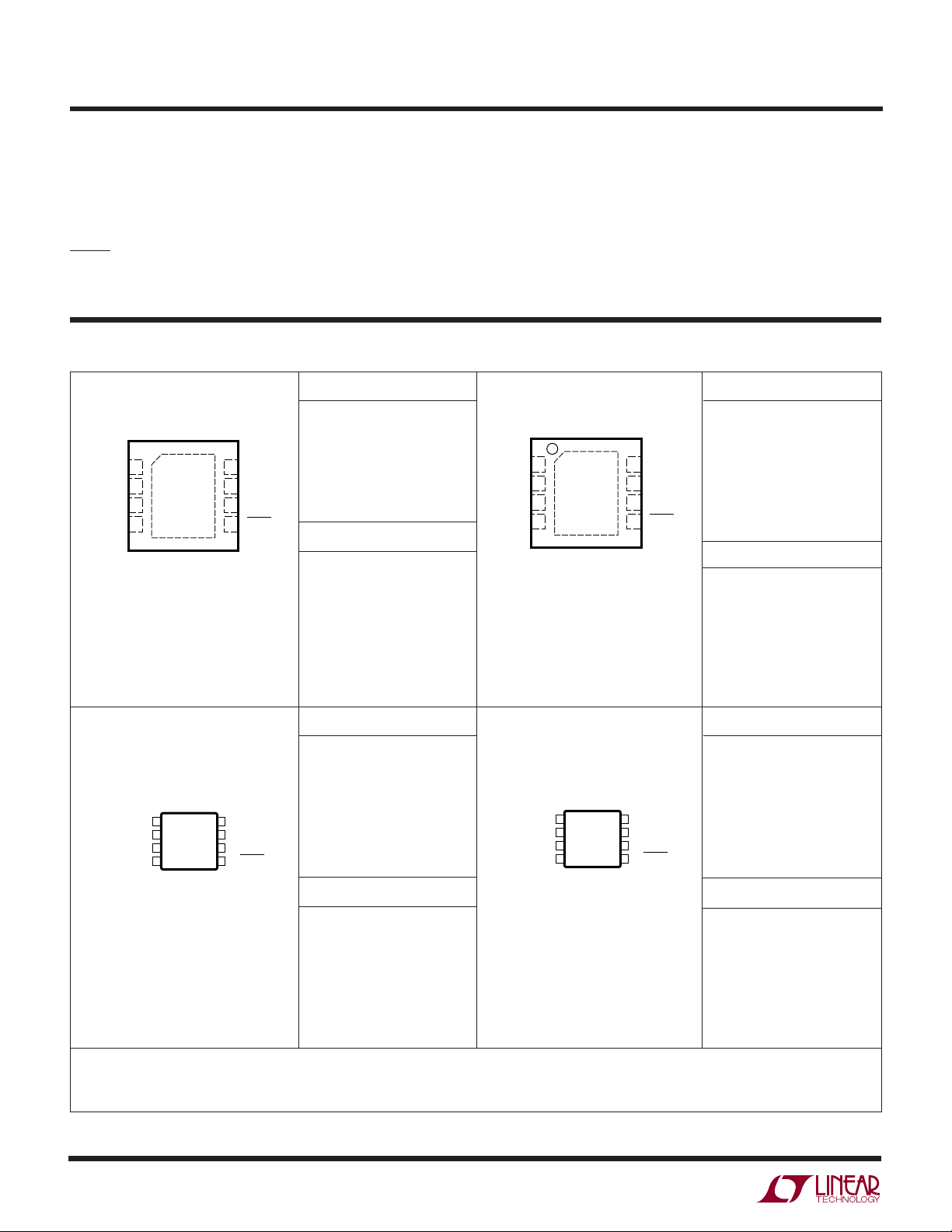
LT3020/LT3020-1.2/
TOP VIEW
9
DD PACKAGE
8-LEAD (3mm × 3mm) PLASTIC DFN
5
6
7
8
4
3
2
1OUT
OUT
ADJ
GND
IN
IN
NC
SHDN
TOP VIEW
9
DD PACKAGE
8-LEAD (3mm × 3mm) PLASTIC DFN
5
6
7
8
4
3
2
1OUT
OUT
OUT
GND
IN
IN
NC
SHDN
LT3020-1.5/LT3020-1.8
WWWU
ABSOLUTE AXI U RATI GS
(Note 1)
IN Pin Voltage ........................................................ ± 10V
OUT Pin Voltage .................................................... ±10V
Input-to-Output Differential Voltage....................... ± 10V
ADJ Pin Voltage .................................................... ±10V
SHDN Pin Voltage ................................................. ± 10V
Output Short-Circut Duration.......................... Indefinite
UU
W
PACKAGE/ORDER I FOR ATIO
ORDER PART NUMBER
LT3020EDD
LT3020IDD
DD PART MARKING
LAEX
T
= 125°C, θJA = 35°C/ W*, θJC = 3°C/ W
JMAX
EXPOSED PAD IS GND (PIN 9) CONNECT TO PIN 4
*SEE THE APPLICATIONS INFORMATION SECTION
LBYH
Operating Junction Temperature Range
(Notes 2, 3) .......................................... –40°C to 125°C
Storage Temperature Range
DD .................................................... – 65°C to 125°C
MS8.................................................. – 65°C to 150°C
Lead Temperature (Soldering, 10 sec)..................300°C
ORDER PART NUMBER
LT3020EDD-1.2
LT3020EDD-1.5
LT3020EDD-1.8
LT3020IDD-1.2
LT3020IDD-1.5
LT3020IDD-1.8
DD PART MARKING
T
= 125°C, θJA = 35°C/ W*, θJC = 3°C/ W
JMAX
EXPOSED PAD IS GND (PIN 9) CONNECT TO PIN 4
*SEE THE APPLICATIONS INFORMATION SECTION
LBKC
LBKD
LBKF
LBYJ
LBYK
LBYM
ORDER PART NUMBER ORDER PART NUMBER
LT3020EMS8
LT3020IMS8
TOP VIEW
IN
OUT
1
OUT
2
ADJ
3
GND
4
MS8 PACKAGE
8-LEAD PLASTIC MSOP
T
= 150°C, θJA = 125°C/ W, θJC = 40°C/ W
JMAX
SEE THE APPLICATIONS INFORMATION SECTION
8
7
6
5
IN
NC
SHDN
MS8 PART MARKING
LTAGL
LTBYN
Order Options Tape and Reel: Add #TR
Lead Free: Add #PBF Lead Free Tape and Reel: Add #TRPBF
Lead Free Part Marking: http://www.linear.com/leadfree/
Consult LTC Marketing for parts specified with wider operating temperature ranges.
TOP VIEW
IN
OUT
1
OUT
2
OUT
3
GND
4
MS8 PACKAGE
8-LEAD PLASTIC MSOP
T
= 150°C, θJA = 125°C/ W, θJC = 40°C/ W
JMAX
SEE THE APPLICATIONS INFORMATION SECTION
8
7
6
5
IN
NC
SHDN
LT3020EMS8-1.2
LT3020EMS8-1.5
LT3020EMS8-1.8
LT3020IMS8-1.2
LT3020IMS8-1.5
LT3020IMS8-1.8
MS8 PART MARKING
LTBKG
LTBKH
LTBKJ
LTBYP
LTBYQ
LTBYR
3020fc
2
LT3020/LT3020-1.2/
LT3020-1.5/LT3020-1.8
ELECTRICAL CHARACTERISTICS
The ● denotes specifications which apply over the full operating temperature range, otherwise specifications are TJ = 25°C.
PARAMETER CONDITIONS MIN TYP MAX UNITS
Minimum Input Voltage (Note 14) I
ADJ Pin Voltage (Notes 4, 5) V
Regulated Output Voltage LT3020-1.2 V
(Note 4) 1.5V < V
Line Regulation (Note 6) ∆V
Load Regulation (Note 6) V
Dropout Voltage (Notes 7, 12) I
GND Pin Current I
= V
V
IN
OUT(NOMINAL)
(Notes 8, 12) I
Output Voltage Noise C
ADJ Pin Bias Current V
Shutdown Threshold V
SHDN Pin Current (Note 10) V
Quiescent Current in Shutdown V
Ripple Rejection (Note 6) VIN – V
= 100mA, TJ > 0°C 0.9 1.05 V
LOAD
= 100mA, TJ < 0°C 0.9 1.10 V
I
LOAD
= 1.5V, I
IN
1.15V < V
LT3020-1.5 V
LT3020-1.8 V
= 1.15V to 10V, I
IN
LT3020-1.2 ∆V
LT3020-1.5 ∆V
LT3020-1.8 ∆V
= 1.15V, ∆I
IN
LT3020-1.2 V
LT3020-1.5 V
LT3020-1.8 V
= 10mA 85 115 mV
LOAD
I
= 10mA
LOAD
I
= 100mA 150 180 mV
LOAD
= 100mA
I
LOAD
= 0mA
LOAD
I
= 1mA 570 µA
LOAD
= 10mA 920 µA
LOAD
= 100mA
I
LOAD
= 2.2µF, I
OUT
= 0.2V,
ADJ
= Off to On
OUT
= On to Off
V
OUT
= 0V, V
SHDN
= 10V, V
V
SHDN
= 6V, V
IN
OUT
LT3020-1.2 VIN – V
= 100mA
I
LOAD
LT3020-1.5 VIN – V
I
= 100mA
LOAD
LT3020-1.8 VIN – V
= 100mA
I
LOAD
= 1mA 196 200 204 mV
LOAD
< 10V, 1mA < I
IN
= 1.5V, I
IN
= 1.8V, I
IN
1.8V < V
= 2.1V, I
IN
2.1V < V
LOAD
IN
IN
IN
= 1mA to 100mA –1 0.4 1 mV
LOAD
= 1.5V, ∆I
IN
= 1.8V, ∆I
IN
= 2.1V, ∆I
IN
= 100mA, BW = 10Hz to 100kHz, V
LOAD
= 1.2V (Notes 6, 9) 20 50 nA
RIPPLE
= 10V
IN
= 10V
IN
= 0V 3 9 µA
SHDN
= 1V, V
RIPPLE
= 1V, V
OUT
= 1V, V
OUT
= 1V, V
OUT
< 100mA
LOAD
= 1mA 1.176 1.200 1.224 V
LOAD
< 10V, 1mA < I
IN
= 1mA 1.470 1.500 1.530 V
LOAD
< 10V, 1mA < I
IN
= 1mA 1.764 1.800 1.836 V
LOAD
< 10V, 1mA < I
IN
= 1mA
= 1.5V to 10V, I
= 1.8V to 10V, I
= 2.1V to 10V, I
= 1mA to 100mA –6 1 6 mV
LOAD
= 1mA to 100mA –7.5 1.5 7.5 mV
LOAD
= 1mA to 100mA –9 2 9 mV
LOAD
= 0.5V
, f
P-P
RIPPLE
RIPPLE
RIPPLE
RIPPLE
= 0.5V
= 0.5V
= 0.5V
LOAD
LOAD
LOAD
= 120Hz, I
LOAD
LOAD
LOAD
= 1mA
= 1mA
= 1mA
, f
P-P
, f
P-P
, f
P-P
●
193 200 206 mV
< 100mA
< 100mA
< 100mA
= 1.2V 245 µV
OUT
= 100mA 64 dB
LOAD
= 120Hz, 60 dB
RIPPLE
= 120Hz, 58 dB
RIPPLE
= 120Hz, 56 dB
RIPPLE
●
1.157 1.200 1.236 V
●
1.447 1.500 1.545 V
●
1.737 1.800 1.854 V
●
–1.75 0 1.75 mV
●
–10.5 0 10.5 mV
●
–13 0 13 mV
●
–15.8 0 15.8 mV
●
●
●
●
●
●
0.25 0.61 V
●
●
120 250 µA
2.25 3.5 mA
0.61 0.9 V
3 9.5 µA
180 mV
285 mV
±1 µA
RMS
3020fc
3
LT3020/LT3020-1.2/
LT3020-1.5/LT3020-1.8
ELECTRICAL CHARACTERISTICS
The ● denotes specifications which apply over the full operating temperature range, otherwise specifications are TJ = 25°C.
PARAMETER CONDITIONS MIN TYP MAX UNITS
Current Limit (Note 12) V
Input Reverse Leakage Current V
Reverse Output Current V
(Notes 11, 13) LT3020-1.2 V
Note 1: Absolute Maximum Ratings are those values beyond which the life
of a device may be impaired.
Note 2: The LT3020 regulators are tested and specified under pulse load
conditions such that T
T
= 25°C. Performance at –40°C and 125°C is assured by design,
A
≈ TA. The LT3020E is 100% production tested at
J
characterization and correlation with statistical process controls. The
LT3020I is guaranteed over the full –40°C to 125°C operating junction
temperature range.
Note 3: This IC includes overtemperature protection that is intended to
protect the device during momentary overload conditions. Junction
temperature will exceed 125°C when overtemperature protection is active.
Continuous operation above the specified maximum operating junction
temperature may impair device reliability.
Note 4: Maximum junction temperature limits operating conditions. The
regulated output voltage specification does not apply for all possible
combinations of input voltage and output current. Limit the output current
range if operating at maximum input voltage. Limit the input voltage range
if operating at maximum output current.
Note 5: Typically the LT3020 supplies 100mA output current with a 1V
input supply. The guaranteed minimum input voltage for 100mA output
current is 1.10V.
Note 6: The LT3020 is tested and specified for these conditions with an
external resistor divider (20k and 30.1k) setting V
resistor divider adds 10µA of output load current. The line regulation and
load regulation specifications refer to the change in the 0.2V reference
voltage, not the 0.5V output voltage. Specifications for fixed output voltage
devices are referred to the output voltage.
= 10V, V
IN
V
= V
IN
= –10V, V
IN
OUT
= 1.2V, V
= 0V 360 mA
OUT
OUT(NOMINAL)
OUT
= 0V 3 5 µA
IN
LT3020-1.5 V
LT3020-1.8 V
to 0.5V. The external
OUT
+ 0.5V, ∆V
OUT
= –5%
●
110 310 mA
= 0V 1 10 µA
OUT
OUT
OUT
= 1.2V, V
= 1.5V, V
= 1.8V, V
= 0V 10 15 µA
IN
= 0V 10 15 µA
IN
= 0V 10 15 µA
IN
Note 7: Dropout voltage is the minimum input to output voltage differential
needed to maintain regulation at a specified output current. In dropout the
output voltage equals: (V
IN
– V
Note 8: GND pin current is tested with V
DROPOUT
).
= V
IN
OUT(NOMINAL)
and a current
source load. The device is tested while operating in its dropout region.
This condition forces the worst-case GND pin current. GND pin current
decreases at higher input voltages.
Note 9: Adjust pin bias current flows out of the ADJ pin.
Note 10: Shutdown pin current flows into the SHDN pin.
Note 11: Reverse output current is tested with IN grounded and OUT
forced to the rated output voltage. This current flows into the OUT pin and
out of the GND pin. For fixed voltage devices this includes the current in
the output resistor divider.
Note 12: The LT3020 is tested and specified for these conditions with an
external resistor divider (20k and 100k) setting V
to 1.2V. The external
OUT
resistor divider adds 10µA of load current.
Note 13: Reverse current is higher for the case of (rated_output) < V
because the no-load recovery circuitry is active in this region and is
V
IN,
OUT
trying to restore the output voltage to its nominal value.
Note 14: Minimum input voltage is the minimum voltage required by the
control circuit to regulate the output voltage and supply the full 100mA
rated current. This specification is tested at V
= 0.5V. At higher output
OUT
voltages the minimum input voltage required for regulation will be equal to
the regulated output voltage V
plus the dropout voltage.
OUT
<
4
3020fc
LT3020/LT3020-1.2/
INPUT VOLTAGE (V)
0
GND PIN CURRENT (µA)
2500
2250
2000
1500
1750
1250
1000
750
500
250
0
8
3020 G06
213579
4
6
10
V
OUT
= 1.2V
T
J
= 25°C
RL = 12Ω
I
L
= 100mA
RL = 24Ω
I
L
= 50mA
RL = 120Ω
I
L
= 10mA
RL = 1.2k, IL = 1mA
TEMPERATURE (°C)
–50
QUIESCENT CURRENT (µA)
250
225
200
150
175
125
100
75
50
25
0
3020 G03
250–25 50 75
125100
V
SHDN
= V
IN
V
SHDN
= 0V
VIN = 6V
V
OUT
= 1.2V
I
L
= 0
LT3020-1.5/LT3020-1.8
UW
TYPICAL PERFOR A CE CHARACTERISTICS
Typical Dropout Voltage Dropout Voltage Quiescent Current
250
225
200
175
150
125
100
75
DROPOUT VOLTAGE (mV)
50
25
0
0
TJ = 125°C
2010 30 50 70 90
OUTPUT CURRENT (mA)
TJ = 25°C
40
60
80
100
3020 G01
250
V
= 1.2V
OUT
225
200
175
150
125
100
75
DROPOUT VOLTAGE (mV)
50
25
0
–50
TEMPERATURE (°C)
250–25 50 75
IL = 100mA
IL = 50mA
IL = 10mA
IL = 1mA
125100
3020 G02
ADJ Pin Voltage
206
IL = 1mA
204
202
200
198
ADJ PIN VOLTAGE (mV)
196
194
–50
250–25 50 75
TEMPERATURE (°C)
Output Voltage
1.230
IL = 1mA
1.220
1.210
1.200
1.190
OUTPUT VOLTAGE (V)
1.180
1.170
–50
–25 0
50 100 125
25 75
TEMPERATURE (°C)
3020 G04
3020 G24
125100
Output Voltage Output Voltage
1.830
IL = 1mA
1.820
1.810
1.800
1.790
OUTPUT VOLTAGE (V)
1.780
1.770
–50
–25 0
Quiescent Current
1000
V
= 1.2V
OUT
= 0
I
900
L
= 25°C
T
J
800
700
600
500
400
300
QUIESCENT CURRENT (µA)
200
100
0
213579
0
50 100 125
25 75
TEMPERATURE (°C)
V
= V
SHDN
IN
V
= 0V
SHDN
6
4
INPUT VOLTAGE (V)
3020 G22
8
3020 G05
OUTPUT VOLTAGE (V)
10
1.530
IL = 1mA
1.520
1.510
1.500
1.490
1.480
1.470
–50
GND Pin Current
–25 0
50 100 125
25 75
TEMPERATURE (°C)
3020 G23
3020fc
5

LT3020/LT3020-1.2/
TEMPERATURE (°C)
–50
SHDN PIN THRESHOLD (V)
1.0
0.9
0.8
0.6
0.7
0.5
0.4
0.3
0.2
0.1
0
3020 G08
250–25 50 75
125100
IL = 1mA
LT3020-1.5/LT3020-1.8
UW
TYPICAL PERFOR A CE CHARACTERISTICS
Quiescent Current
1000
900
800
700
600
500
400
300
QUIESCENT CURRENT (µA)
200
100
0
0123
GND Pin Current
2500
2250
2000
1750
1500
1250
1000
750
GND PIN CURRENT (µA)
500
250
0
0123
V
IL = 0
TJ = 25°C
V
V
4
5
INPUT VOLTAGE (V)
V
TJ = 25°C
RL = 18Ω
= 100mA
I
L
RL = 36Ω
I
= 50mA
L
RL = 180Ω
= 10mA
I
L
4
5
INPUT VOLTAGE (V)
= 1.5V (LT 3020-1.5)
OUT
= V
SHDN
IN
= 0V
SHDN
678910
3020 G27
= 1.8V (LT 3020-1.8)
OUT
RL = 1.8k
= 1mA
I
L
678910
3020 G26
GND Pin Current
2500
2250
GND PIN CURRENT (µA)
2000
1750
1500
1250
1000
750
500
250
0
RL = 15Ω
I
L
RL = 30Ω
= 50mA
I
L
RL = 150Ω
= 10mA
I
L
0123
GND Pin Current vs I
2000
VIN = 1.7V
= 1.2V
V
1800
OUT
= 25°C
T
J
1600
1400
1200
1000
800
600
GND PIN CURRENT (µA)
400
200
0
2010 30 50 70 90
0
V
= 1.5V (LT 3020-1.5)
OUT
TJ = 25°C
= 100mA
RL = 1.5k
= 1mA
I
L
4
678910
5
INPUT VOLTAGE (V)
LOAD
60
40
OUTPUT CURRENT (mA)
Quiescent Current
3020 G28
1000
900
800
700
600
500
400
300
QUIESCENT CURRENT (µA)
200
100
0
0123
V
= 1.8V (LT 3020-1.8)
OUT
IL = 0
TJ = 25°C
V
= V
SHDN
V
= 0V
SHDN
4
678910
5
INPUT VOLTAGE (V)
IN
3020 G25
SHDN Pin Threshold
80
100
3020 G07
SHDN Pin Input Current
5.0
4.5
4.0
3.5
3.0
2.5
2.0
1.5
6
1.0
SHDN PIN INPUT CURRENT (µA)
0.5
0
0
TJ = 25°C
213579
SHDN PIN VOLTAGE (V)
6
4
SHDN Pin Input Current (µA)
5.0
V
= 10V
SHDN
4.5
4.0
3.5
3.0
2.5
2.0
1.5
1.0
SHDN PIN INPUT CURRENT (µA)
0.5
0
8
10
3020 G09
0
–50
250–25 50 75
TEMPERATURE (°C)
125100
3020 G10
ADJ Pin Bias Current
25
20
15
10
ADJ PIN BIAS CURRENT (nA)
5
0
–50
250–25 50 75
TEMPERATURE (°C)
125100
3020 G11
3020fc

TEMPERATURE (°C)
–50
LOAD REGULATION (mV)
1.0
0.8
0.6
0.2
0.4
0
–0.2
–0.4
–0.6
–0.8
–1.0
3020 G17
250–25 50 75
125100
VIN = 1.15V
V
OUT
= 0.5V
*LOAD REGULATION NUMBER REFERS
TO CHANGE IN THE 200mV REFERENCE
VOLTAGE
UW
FREQUENCY (Hz)
10
OUTPUT NOISE SPECTRAL DENSITY (µV/√Hz)
10
1
0.1
0.01
1k 100k 1M100 10k
3020 G18
V
OUT
= 1.2V
I
L
= 100mA
C
OUT
= 2.2µF
TYPICAL PERFOR A CE CHARACTERISTICS
LT3020/LT3020-1.2/
LT3020-1.5/LT3020-1.8
Current Limit
500
V
= 0V
OUT
450
400
350
300
250
200
150
CURRENT LIMIT (mA)
100
50
0
0
–50
VIN = 10V
VIN = 1.7V
TEMPERATURE (°C)
Input Ripple Rejection
100
90
80
70
60
50
40
30
RIPPLE REJECTION (dB)
20
VIN = 1.5V + 0.5V
= 0.5V
V
10
OUT
= 100mA
I
L
0
–50
TEMPERATURE (°C)
250–25 50 75
RIPPLE AT f = 120Hz
P-P
250–25 50 75
3020 G12
3020 G15
Reverse Output Current
500
VIN = 0V
= 1.2V
V
450
OUT
400
350
300
250
200
150
100
REVERSE OUTPUT CURRENT (µA)
50
0
0
125100
–50
250–25 50 75
TEMPERATURE (°C)
125100
3020 G13
Input Ripple Rejection
70
60
50
40
C
30
20
RIPPLE REJECTION (dB)
VIN = 1.5V + 50mV
10
= 0.5V
V
OUT
= 100mA
I
L
0
10 1k 10k 1M
100
RIPPLE
RMS
FREQUENCY (Hz)
OUT
C
OUT
= 10µF
= 2.2µF
100k
3020 G14
Load Regulation
Minimum Input Voltage
1.1
IL = 100mA
1.0
0.9
0.8
0.7
0.6
0.5
0.4
0.3
MINIMUM INPUT VOLTAGE (V)
0.2
0.1
0
125100
–50
250–25 50 75
TEMPERATURE (°C)
125100
3020 G16
∆IL = 1mA to 100mA
V
OUT
50mV/DIV
I
OUT
100mA/DIV
Transient Response
I
= 10mA TO 100mA
OUT
= 1.5V
V
OUT
50µs/DIV
Output Noise Spectral Density
3020 G21
3020fc
7

LT3020/LT3020-1.2/
LT3020-1.5/LT3020-1.8
UW
TYPICAL PERFOR A CE CHARACTERISTICS
RMS Output Noise vs Load
Current (10Hz to 100kHz)
300
V
= 1.2V
OUT
= 2.2µF
C
OUT
250
)
RMS
200
150
100
OUTPUT NOISE (µV
50
0
0.01 1 10 100
0.1
LOAD CURRENT (mA)
3020 G19
No-Load Recovery Threshold
18
16
14
12
10
8
6
4
OUTPUT CURRENT SINK (mA)
2
0
0
OUTPUT OVERSHOOT (%)
15105
20
3020 G20
U
UU
PI FU CTIO S
OUT (Pins 1, 2): These pins supply power to the load. Use
a minimum output capacitor of 2.2µF to prevent oscillations.
Applications with large load transients require larger output capacitors to limit peak voltage transients. See the
Applications Information section for more information on
output capacitance and reverse output characteristics.
OUT (Pin 3, Fixed Voltage Device Only): This pin is the
sense point for the internal resistor divider. It should be
tied directly to the other OUT pins (1, 2) for best results.
ADJ (Pin 3, Adjustable Device Only): This pin is the
inverting terminal to the error amplifier. Its typical input
bias current of 20nA flows out of the pin (see curve of ADJ
Pin Bias Current vs Temperature in the Typical Performance Characteristics). The ADJ pin reference voltage is
200mV (referred to GND).
GND (Pin 4): Ground.
SHDN (Pin 5): The SHDN pin puts the LT3020 into a low
power state. Pulling the SHDN pin low turns the output off.
Drive the SHDN pin with either logic or an open collector/
drain device with a pull-up resistor. The pull-up resistor
supplies the pull-up current to the open collector/drain
logic, normally several microamperes, and the SHDN pin
current, typically 2.3µA. If unused, connect the SHDN pin
to VIN. The LT3020 does not function if the SHDN pin is not
connected.
IN (Pins 7, 8): These pins supply power to the device. The
LT3020 requires a bypass capacitor at IN if it is more than
six inches away from the main input filter capacitor. The
output impedance of a battery rises with frequency, so
include a bypass capacitor in battery-powered circuits. A
bypass capacitor in the range of 2.2µF to 10µF suffices. The
LT3020 withstands reverse voltages on the IN pin with
respect to ground and the OUT pin. In the case of a reversed
input, which occurs if a battery is plugged in backwards,
the LT3020 acts as if a diode is in series with its input. No
reverse current flows into the LT3020 and no reverse voltage appears at the load. The device protects itself and the
load.
GND (Pin 9, DD8 Package Only): Ground. Solder Pin 9
(the exposed pad) to the PCB. Connect directly to Pin 4 for
best performance.
8
3020fc

BLOCK DIAGRA
SHDN
(5)
SHUTDOWN
W
THERMAL
SHUTDOWN
LT3020/LT3020-1.2/
LT3020-1.5/LT3020-1.8
IN
(7, 8)
R3
D1
–
ERROR AMP
+
–
NO-LOAD
RECOVERY
BIAS CURRENT
AND
REFERENCE
GENERATOR
200mV
212mV
+
NOTE:
FOR LT3020 ADJUST PIN 3 IS CONNECTED TO
THE ADJUST PIN, R1 AND R2 ARE EXTERNAL.
FOR LT3020-1.X PIN 3 IS CONNECTED TO THE
OUTPUT SENSE PIN, R1 AND R2 ARE INTERNAL.
WUUU
APPLICATIO S I FOR ATIO
The LT3020 is a very low dropout linear regulator capable
of 0.9V input supply operation. Devices supply 100mA of
output current and dropout voltage is typically 150mV.
Quiescent current is typically 120µA and drops to 3µA in
shutdown. The LT3020 incorporates several protection
features, making it ideal for use in battery-powered systems. The device protects itself against reverse-input and
reverse-output voltages. In battery backup applications
where the output is held up by a backup battery when the
input is pulled to ground, the LT3020 acts as if a diode is
in series with its output which prevents reverse current
flow. In dual supply applications where the regulator load
is returned to a negative supply, the output can be pulled
below ground by as much as 10V without affecting startup or normal operation.
Adjustable Operation
The LT3020’s output voltage range is 0.2V to 9.5V. Figure
1 shows that the output voltage is set by the ratio of two
external resistors. The device regulates the output to
maintain the ADJ pin voltage at 200mV referenced to
ground. The current in R1 equals 200mV/R1 and the
Q3
CURRENT
FIXED
V
OUT
1.2V
1.5V
1.8V
GAIN
R1
20k
20k
20k
R2
100k
130k
160k
Q1
D2
Q2
R2
25k
R1
3020 BD
OUT
(1, 2)
OUT SENSE
(3)
ADJ
(3)
GND
(4,9)
current in R2 is the current in R1 minus the ADJ pin bias
current. The ADJ pin bias current of 20nA flows out of the
pin. Use the formula in Figure 1 to calculate output voltage.
An R1 value of 20k sets the resistor divider current to
10µA. Note that in shutdown the output is turned off and
the divider current is zero. Curves of ADJ Pin Voltage vs
Temperature and ADJ Pin Bias Current vs Temperature
appear in the Typical Performance Characteristics section.
Specifications for output voltages greater than 200mV are
proportional to the ratio of desired output voltage to
200mV; (V
/200mV). For example, load regulation for
OUT
IN
V
IN
SHDN
= 200mV
V
OUT
= 200mV
V
ADJ
= 20nA AT 25°C
I
ADJ
OUTPUT RANGE = 0.2V TO 9.5V
OUT
LT3020-ADJ
ADJ
GND
R2
1 + – I
()
R1
ADJ
R2
R1
3020 F01
(R2)
V
OUT
+
Figure 1. Adjustable Operation
3020fc
9

LT3020/LT3020-1.2/
LT3020-1.5/LT3020-1.8
WUUU
APPLICATIO S I FOR ATIO
an output current change of 1mA to 100mA is typically
0.4mV at V
= 200mV. At V
ADJ
(1.5V/200mV) • (0.4mV) = 3mV
= 1.5V, load regulation is:
OUT
–20
20
0
BOTH CAPACITORS ARE 16V,
1210 CASE SIZE, 10µF
X5R
Output Capacitance and Transient Response
The LT3020’s design is stable with a wide range of output
capacitors, but is optimized for low ESR ceramic capacitors. The output capacitor’s ESR affects stability, most
notably with small value capacitors. Use a minimum
output capacitor of 2.2µF with an ESR of 0.3Ω or less to
prevent oscillations. The LT3020 is a low voltage device,
and output load transient response is a function of output
capacitance. Larger values of output capacitance decrease
the peak deviations and provide improved transient response for larger load current changes. For output capacitor values greater than 20µF a small feedforward capacitor
with a value of 300pF across the upper divider resistor (R2
in Figure 1) is required.
Give extra consideration to the use of ceramic capacitors.
Manufacturers make ceramic capacitors with a variety of
dielectrics, each with a different behavior across temperature and applied voltage. The most common dielectrics are
Z5U, Y5V, X5R and X7R. The Z5U and Y5V dielectrics
provide high C-V products in a small package at low cost,
but exhibit strong voltage and temperature coefficients.
The X5R and X7R dielectrics yield highly stable
characterisitics and are more suitable for use as the output
capacitor at fractionally increased cost. The X5R and X7R
dielectrics both exhibit excellent voltage coefficient characteristics. The X7R type works over a larger temperature
range and exhibits better temperature stability whereas
X5R is less expensive and is available in higher values.
Figures 2 and 3 show voltage coefficient and temperature
coefficient comparisons between Y5V and X5R material.
–40
–60
CHANGE IN VALUE (%)
–80
–100
0
26
4
DC BIAS VOLTAGE (V)
Y5V
14
8
12
10
16
3020 F02
Figure 2. Ceramic Capacitor DC Bias Characteristics
40
20
0
–20
–40
–60
CHANGE IN VALUE (%)
–80
BOTH CAPACITORS ARE 16V,
1210 CASE SIZE, 10µF
–100
–50
–25 0
25 75
TEMPERATURE (°C)
X5R
Y5V
50 100 125
3020 F03
Figure 3. Ceramic Capacitor Temperature Characteristics
Voltage and temperature coefficients are not the only
sources of problems. Some ceramic capacitors have a
piezoelectric response. A piezoelectric device generates
voltage across its terminals due to mechanical stress, similar to the way a piezoelectric accelerometer or microphone
works. For a ceramic capacitor, the stress can be induced
by vibrations in the system or thermal transients. The resulting voltages produced can cause appreciable amounts
of noise. A ceramic capacitor produced Figure 4’s trace in
10
1mV/DIV
V
C
I
LOAD
OUT
OUT
= 1.3V
= 10µF
= 0
1ms/DIV 3020 F04
Figure 4. Noise Resulting from Tapping on a Ceramic Capacitor
3020fc

WUUU
APPLICATIO S I FOR ATIO
LT3020/LT3020-1.2/
LT3020-1.5/LT3020-1.8
response to light tapping from a pencil. Similar vibration
induced behavior can masquerade as increased output
voltage noise.
No-Load/Light-Load Recovery
A possible transient load step that occurs is where the
output current changes from its maximum level to zero
current or a very small load current. The output voltage
responds by overshooting until the regulator lowers the
amount of current it delivers to the new level. The regulator
loop response time and the amount of output capacitance
control the amount of overshoot. Once the regulator has
decreased its output current, the current provided by the
resistor divider (which sets V
) is the only current
OUT
remaining to discharge the output capacitor from the level
to which it overshot. The amount of time it takes for the
output voltage to recover easily extends to milliseconds
with microamperes of divider current and a few microfarads of output capacitance.
To eliminate this problem, the LT3020 incorporates a
no-load or light-load recovery circuit. This circuit is a
voltage-controlled current sink that significantly improves
the light load transient response time by discharging the
output capacitor quickly and then turning off. The current
sink turns on when the output voltage exceeds 6% of the
nominal output voltage. The current sink level is then
proportional to the overdrive above the threshold up to a
maximum of approximately 15mA. Consult the curve in
the Typical Performance Characteristics for the No-Load
Recovery Threshold.
If external circuitry forces the output above the no load
recovery circuit’s threshold, the current sink turns on in an
attempt to restore the output voltage to nominal. The
current sink remains on until the external circuitry releases
the output. However, if the external circuitry pulls the
output voltage above the input voltage, or the input falls
below the output, the LT3020 turns the current sink off and
shuts down the bias current/reference generator circuitry.
Thermal Considerations
The LT3020’s power handling capability is limited by its
maximum rated junction temperature of 125°C. The power
dissipated by the device is comprised of two components:
1. Output current multiplied by the input-to-output voltage differential: (I
OUT
IN
– V
OUT
) and
)(V
2. GND pin current multiplied by the input voltage:
(I
)(VIN).
GND
GND pin current is found by examining the GND pin
current curves in the Typical Performance Characteristics.
Power dissipation is equal to the sum of the two components listed above.
The LT3020 regulator has internal thermal limiting (with
hysteresis) designed to protect the device during overload
conditions. For normal continuous conditions, do not
exceed the maximum junction temperature rating of 125°C.
Carefully consider all sources of thermal resistance from
junction to ambient including other heat sources mounted
in proximity to the LT3020.
The underside of the LT3020 DD package has exposed metal
(4mm2) from the lead frame to where the die is attached.
This allows heat to directly transfer from the die junction
to the printed circuit board metal to control maximum
operating junction temperature. The dual-in-line pin arrangement allows metal to extend beyond the ends of the
package on the topside (component side) of a PCB. Connect this metal to GND on the PCB. The multiple IN and OUT
pins of the LT3020 also assist in spreading heat to the PCB.
The LT3020 MS8 package has pin 4 fused with the lead
frame. This also allows heat to transfer from the die to the
printed circuit board metal, therefore reducing the thermal
resistance. Copper board stiffeners and plated throughholes can also be used to spread the heat generated by
power devices.
The following tables list thermal resistance for several
different board sizes and copper areas for two different
packages. Measurements were taken in still air on 3/32"
FR-4 board with one ounce copper.
Table 1. Measured Thermal Resistance for DD Package
COPPER AREA THERMAL RESISTANCE
TOPSIDE* BACKSIDE BOARD AREA (JUNCTION-TO-AMBIENT)
2500mm22500mm
2
900mm
225mm
100mm
50mm
2500mm
2
2500mm
2
2500mm
2
2500mm
2
2
2
2
2
2500mm
2500mm
2500mm
2500mm
2500mm
2
2
2
2
2
35°C/W
40°C/W
55°C/W
60°C/W
70°C/W
3020fc
11

LT3020/LT3020-1.2/
LT3020-1.5/LT3020-1.8
WUUU
APPLICATIO S I FOR ATIO
Table 2. Measured Thermal Resistance for MS8 Package
COPPER AREA THERMAL RESISTANCE
TOPSIDE* BACKSIDE BOARD AREA (JUNCTION-TO-AMBIENT)
2500mm22500mm
1000mm22500mm
225mm22500mm
100mm22500mm
2
50mm
*Device is mounted on topside.
2500mm
2
2500mm
2
2500mm
2
2500mm
2
2500mm
2
2500mm
2
2
2
2
2
110°C/W
115°C/W
120°C/W
130°C/W
140°C/W
Calculating Junction Temperature
Example: Given an output voltage of 1.8V, an input voltage
range of 2.25V to 2.75V, an output current range of 1mA
to 100mA, and a maximum ambient temperature of 70°C,
what will the maximum junction temperature be for an
application using the DD package?
The power dissipated by the device is equal to:
I
OUT(MAX)(VIN(MAX)
– V
OUT
) + I
GND(VIN(MAX)
)
where
at (I
= 100mA
= 2.75V
= 100mA, V
OUT
= 2.75V) = 3mA
IN
I
OUT(MAX)
V
IN(MAX)
I
GND
so
P = 100mA(2.75V – 1.8V) + 3mA(2.75V) = 0.103W
The thermal resistance is in the range of 35°C/W to
70°C/W depending on the copper area. So the junction
temperature rise above ambient is approximately equal to:
0.103W(52.5°C/W) = 5.4°C
The maximum junction temperature equals the maximum
junction temperature rise above ambient plus the maximum ambient temperature or:
= 70°C + 5.4°C = 75.4°C
T
JMAX
Protection Features
The LT3020 incorporates several protection features that
make it ideal for use in battery-powered circuits. In addition to the normal protection features associated with
monolithic regulators, such as current limiting and thermal limiting, the device also protects against reverseinput voltages, reverse-output voltages and reverse
output-to-input voltages.
Current limit protection and thermal overload protection
protect the device against current overload conditions at
the output of the device. For normal operation, do not
exceed a junction temperature of 125°C.
The IN pins of the device withstand reverse voltages of
10V. The LT3020 limits current flow to less than 1µA and
no negative voltage appears at OUT. The device protects
both itself and the load against batteries that are plugged
in backwards.
The LT3020 incurs no damage if OUT is pulled below
ground. If IN is left open circuit or grounded, OUT can be
pulled below ground by 10V. No current flows from the
pass transistor connected to OUT. However, current flows
in (but is limited by) the resistor divider that sets the output
voltage. Current flows from the bottom resistor in the
divider and from the ADJ pin’s internal clamp through the
top resistor in the divider to the external circuitry pulling
OUT below ground. If IN is powered by a voltage source,
OUT sources current equal to its current limit capability
and the LT3020 protects itself by thermal limiting. In this
case, grounding SHDN turns off the LT3020 and stops
OUT from sourcing current.
The LT3020 incurs no damage if the ADJ pin is pulled
above or below ground by 10V. If IN is left open circuit or
grounded and ADJ is pulled above ground, ADJ acts like a
25k resistor in series with a 1V clamp (one Schottky diode
in series with one diode). ADJ acts like a 25k resistor in
series with a Schottky diode if pulled below ground. If IN
is powered by a voltage source and ADJ is pulled below its
reference voltage, the LT3020 attempts to source its
current limit capability at OUT. The output voltage increases to VIN – V
DROPOUT
with V
DROPOUT
set by whatever
load current the LT3020 supports. This condition can
potentially damage external circuitry powered by the
LT3020 if the output voltage increases to an unregulated
high voltage. If IN is powered by a voltage source and ADJ
is pulled above its reference voltage, two situations can
occur. If ADJ is pulled slightly above its reference voltage,
the LT3020 turns off the pass transistor, no output current
is sourced and the output voltage decreases to either the
voltage at ADJ or less. If ADJ is pulled above its no load
recovery threshold, the no load recovery circuitry turns on
and attempts to sink current. OUT is actively pulled low
3020fc
12

WUUU
APPLICATIO S I FOR ATIO
LT3020/LT3020-1.2/
LT3020-1.5/LT3020-1.8
and the output voltage clamps at a Schottky diode above
ground. Please note that the behavior described above
applies to the LT3020 only. If a resistor divider is connected under the same conditions, there will be additional
V/R current.
In circuits where a backup battery is required, several
different input/output conditions can occur. The output
voltage may be held up while the input is either pulled to
ground, pulled to some intermediate voltage or is left open
circuit. In the case where the input is grounded, there is
less than 1µA of reverse output current.
If the LT3020 IN pin is forced below the OUT pin or the OUT
pin is pulled above the IN pin, input current drops to less
than 10µA typically. This occurs if the LT3020 input is
connected to a discharged (low voltage) battery and either
a backup battery or a second regulator circuit holds up the
output. The state of the SHDN pin has no effect on the
reverse output current if OUT is pulled above IN.
Input Capacitance and Stability
The LT3020 is designed to be stable with a minimum
capacitance of 2.2µF placed at the IN pin. Ceramic capaci-
tors with very low ESR may be used. However, in cases
where a long wire is used to connect a power supply to the
input of the LT3020 (and also from the ground of the
LT3020 back to the power supply ground), use of low
value input capacitors combined with an output load
current of 20mA or greater may result in an unstable
application. This is due to the inductance of the wire
forming an LC tank circuit with the input capacitor and not
a result of the LT3020 being unstable.
The self-inductance, or isolated inductance, of a wire is
directly proportional to its length. However, the diameter
of a wire does not have a major influence on its selfinductance. For example, the self inductance of a 2-AWG
isolated wire with a diameter of 0.26 in. is about half the
inductance of a 30-AWG wire with a diameter of 0.01 in.
One foot of 30-AWG wire has 465nH of self inductance.
The overall self-inductance of a wire can be reduced in two
ways. One is to divide the current flowing towards the
LT3020 between two parallel conductors. In this case, the
farther the wires are placed apart from each other, the
more inductance will be reduced, up to a 50% reduction
when placed a few inches apart. Splitting the wires basically connects two equal inductors in parallel. However,
when placed in close proximity from each other, mutual
inductance is added to the overall self inductance of the
wires. The most effective way to reduce overall inductance
is to place the forward and return-current conductors (the
wire for the input and the wire for ground) in very close
proximity. Two 30-AWG wires separated by 0.02 in. reduce the overall self-inductance to about one-fifth of a
single isolated wire.
If the LT3020 is powered by a battery mounted in close
proximity on the same circuit board, a 2.2µF input capaci-
tor is sufficient for stability. However, if the LT3020 is
powered by a distant supply, use a larger value input
capacitor following the guideline of roughly 1µF (in addi-
tion to the 2.2µF minimum) per 8 inches of wire length. As
power supply output impedance may vary, the minimum
input capacitance needed to stabilize the application may
also vary. Extra capacitance may also be placed directly on
the output of the power supply; however, this will require
an order of magnitude more capacitance as opposed to
placing extra capacitance in close proximity to the LT3020.
Furthermore, series resistance may be placed between the
supply and the input of the LT3020 to stabilize the application; as little as 0.1Ω to 0.5Ω will suffice.
3020fc
13

LT3020/LT3020-1.2/
LT3020-1.5/LT3020-1.8
PACKAGE DESCRIPTIO
U
DD Package
8-Lead Plastic DFN (3mm × 3mm)
(Reference LTC DWG # 05-08-1698)
0.675 ±0.05
3.5 ±0.05
1.65 ±0.05
(2 SIDES)2.15 ±0.05
PACKAGE
OUTLINE
0.25 ± 0.05
RECOMMENDED SOLDER PAD PITCH AND DIMENSIONS
PIN 1
TOP MARK
(NOTE 6)
0.200 REF
NOTE:
1. DRAWING TO BE MADE A JEDEC PACKAGE OUTLINE M0-229 VARIATION OF (WEED-1)
2. DRAWING NOT TO SCALE
3. ALL DIMENSIONS ARE IN MILLIMETERS
4. DIMENSIONS OF EXPOSED PAD ON BOTTOM OF PACKAGE DO NOT INCLUDE
MOLD FLASH. MOLD FLASH, IF PRESENT, SHALL NOT EXCEED 0.15mm ON ANY SIDE
5. EXPOSED PAD SHALL BE SOLDER PLATED
6. SHADED AREA IS ONLY A REFERENCE FOR PIN 1 LOCATION
ON TOP AND BOTTOM OF PACKAGE
2.38 ±0.05
(2 SIDES)
0.50
BSC
3.00 ±0.10
(4 SIDES)
0.75 ±0.05
0.00 – 0.05
1.65 ± 0.10
(2 SIDES)
R = 0.115
TYP
0.25 ± 0.05
2.38 ±0.10
(2 SIDES)
BOTTOM VIEW—EXPOSED PAD
0.38 ± 0.10
85
14
0.50 BSC
(DD8) DFN 1203
14
3020fc

PACKAGE DESCRIPTIO
U
MS8 Package
8-Lead Plastic MSOP
(Reference LTC DWG # 05-08-1660)
0.889 ± 0.127
(.035 ± .005)
LT3020/LT3020-1.2/
LT3020-1.5/LT3020-1.8
5.23
(.206)
MIN
0.42 ± 0.038
(.0165 ± .0015)
TYP
RECOMMENDED SOLDER PAD LAYOUT
0.254
(.010)
GAUGE PLANE
0.18
(.007)
NOTE:
1. DIMENSIONS IN MILLIMETER/(INCH)
2. DRAWING NOT TO SCALE
3. DIMENSION DOES NOT INCLUDE MOLD FLASH, PROTRUSIONS OR GATE BURRS.
MOLD FLASH, PROTRUSIONS OR GATE BURRS SHALL NOT EXCEED 0.152mm (.006") PER SIDE
4. DIMENSION DOES NOT INCLUDE INTERLEAD FLASH OR PROTRUSIONS.
INTERLEAD FLASH OR PROTRUSIONS SHALL NOT EXCEED 0.152mm (.006") PER SIDE
5. LEAD COPLANARITY (BOTTOM OF LEADS AFTER FORMING) SHALL BE 0.102mm (.004") MAX
DETAIL “A”
(.126 – .136)
(.0256)
° – 6° TYP
0
DETAIL “A”
3.20 – 3.45
0.65
BSC
0.53 ± 0.152
(.021 ± .006)
SEATING
PLANE
3.00 ± 0.102
(.118 ± .004)
(NOTE 3)
4.90
± 0.152
(.193 ± .006)
0.22 – 0.38
(.009 – .015)
TYP
1.10
(.043)
MAX
8
12
0.65
(.0256)
BSC
7
6
3
5
4
0.52
(.0205)
REF
3.00 ± 0.102
(.118 ± .004)
(NOTE 4)
0.86
(.034)
REF
0.127 ± 0.076
(.005 ± .003)
MSOP (MS8) 0204
Information furnished by Linear Technology Corporation is believed to be accurate and reliable.
However, no responsibility is assumed for its use. Linear Technology Corporation makes no representation that the interconnection of its circuits as described herein will not infringe on existing patent rights.
3020fc
15

LT3020/LT3020-1.2/
LT3020-1.5/LT3020-1.8
RELATED PARTS
PART NUMBER DESCRIPTION COMMENTS
LT1121/LT1121HV 150mA, Micropower LDOs VIN: 4.2V to 30V/36V, V
= 16µA, Reverse-Battery Protection, SOT-223, S8, Z Packages
I
SD
LT1129 700mA, Micropower LDO VIN: 4.2V to 30V, V
DD, SOT-223, S8, TO220-5, TSSOP20 Packages
LT1761 100mA, Low Noise Micropower LDO VIN: 1.8V to 20V, V
Low Noise: < 20µV
ThinSOT Package
LT1762 150mA, Low Noise Micropower LDO VIN: 1.8V to 20V, V
Low Noise: <20µV
LT1763 500mA, Low Noise Micropower LDO VIN: 1.8V to 20V, V
Low Noise: < 20µV
LT1764/LT1764A 3A, Low Noise, Fast Transient Response LDOs VIN: 2.7V to 20V, V
Low Noise: <40µV
DD, TO220-5 Packages
LTC1844 150mA, Low Noise, Micropower VLDO VIN: 1.6V to 6.5V, V
Low Noise: < 30µV
LT1962 300mA, Low Noise Micropower LDO VIN: 1.8V to 20V, V
Low Noise: < 20µV
LT1963/LT1963A 1.5A, Low Noise, Fast Transient Response LDOs VIN: 2.1V to 20V, V
Low Noise: < 40µV
DD, TO220-5, SOT223, S8 Packages
LT1964 200mA, Low Noise Micropower, Negative LDO VIN: –2.2V to –20V, V
Low Noise: <30µV
ThinSOT Package
LT3010 50mA, High Voltage, Micropower LDO VIN: 3V to 80V, V
Low Noise: <100µV
MS8E Package
LTC3025 300mA, Low Voltage, Micropower LDO VIN: 0.9V to 5.5V, V
1µF Ceramic Capacitors, DFN-6 Package
LT3150 Low VIN, Fast Transient Response, VLDO Controller VIN: 1.1V to 10V, V
, 1.4MHz Boost Converter Generates Gate Drive, SSOP16 Package
R
DS(ON)
OUT(MIN)
OUT(MIN)
RMS
OUT(MIN)
RMS
OUT(MIN)
RMS
OUT(MIN)
RMS
OUT(MIN)
RMS
OUT(MIN)
RMS
OUT(MIN)
RMS
OUT(MIN)
RMS
OUT(MIN)
RMS
OUT(MIN)
OUT(MIN)
OUT(MIN)
= 3.75V, V
= 1.22V, V
= 3.75V, V
= 0.42V, IQ = 30µA,
DO
= 0.4V, IQ = 50µA, I
DO
= 0.3V, IQ = 20µA, I
DO
SD
SD
= 16µA,
< 1µA,
, Stable with 1µF Ceramic Capacitor,
= 1.22V, V
= 0.3V, IQ = 25µA, I
DO
SD
< 1µA,
, MS8 Package
= 1.22V, V
= 0.3V, IQ = 30µA, I
DO
SD
< 1µA,
, S8 Package
= 1.21V, V
= 0.34V, IQ = 1mA, I
DO
SD
< 1µA,
, “A” Version Stable with Ceramic Capacitors,
= 1.25V, V
= 0.09V, IQ = 35µA, ISD < 1µA,
DO
, ThinSOT Package
= 1.22V, V
= 0.27V, IQ = 30µA, I
DO
SD
< 1µA,
, MS8 Package
= 1.21V, V
= 0.34V, IQ = 1mA, I
DO
SD
< 1µA,
, “A” Version Stable with Ceramic Capacitors,
= 1.21V, V
= 0.34V, IQ = 30µA, I
DO
SD
= 3µA,
, Stable with Ceramic Capacitors,
= 1.2V, V
= 0.3V, IQ = 30µA, I
DO
SD
< 1µA,
, Stable with 1µF Output Capacitor, Exposed
= 0.4V, V
= 1.23V, V
= 0.05V, IQ = 54µA, Stable with
DO
= Set by External MOSFET
DO
16
Linear Technology Corporation
1630 McCarthy Blvd., Milpitas, CA 95035-7417
(408) 432-1900 ● FAX: (408) 434-0507
●
www.linear.com
3020fc
LT/LT 0905 REV C • PRINTED IN USA
© LINEAR TECHNOLOGY CORPORATION 2004
 Loading...