

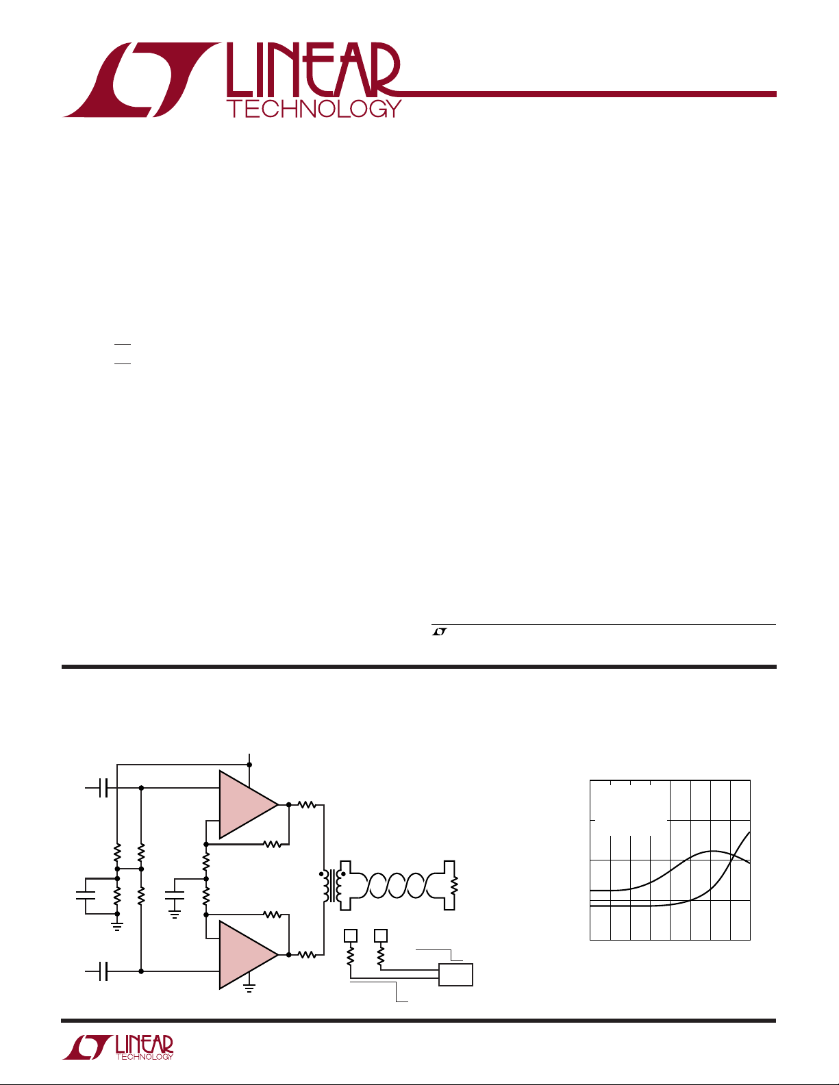
Adjustable Current Operational Amplifier
LINE VOLTAGE (V
P-P
)
0
HARMONIC DISTORTION (dBc)
–60
–70
–80
–90
–100
1969 TA01b
2 4 6 8 10 12 14 16
VS = 12V
A
V
= 10
f = 200kHz
100Ω LINE
1:2 TRANSFORMER
HD2
HD3
FEATURES
■
700MHz Gain Bandwidth
■
±200mA Minimum I
■
Adjustable Quiescent Current
■
Low Distortion: –72dBc at 1MHz, 4V
■
Stable in AV ≥ 10, Simple Compensation for AV < 10
■
±4.3V Minimum Output Swing, VS = ±6V, RL = 25Ω
■
Stable with 1000pF Load
■
6nV/√Hz Input Noise Voltage
■
2pA/√Hz Input Noise Current
■
4mV Maximum Input Offset Voltage
■
4µA Maximum Input Bias Current
■
400nA Maximum Input Offset Current
■
±4.5V Minimum Input CMR, VS = ±6V
■
Specified at ±6V, ±2.5V
OUT
, 25Ω, AV = 2
P-P
U
APPLICATIO S
■
DSL Modems
■
xDSL PCI Cards
■
USB Modems
■
Line Drivers
LT1969
Dual 700MHz, 200mA,
U
DESCRIPTIO
The LT®1969 is an adjustable current version of the
popular LT1886, a 200mA minimum output current, dual
op amp with outstanding distortion performance. The
adjustable current feature is highly desirable in applications where minimum power dissipation is required while
still being able to provide adequate line termination.
At nominal supply current, the amplifiers are gain of 10
stable and can easily be compensated for lower gains. The
LT1969 features balanced high impedance inputs with
4µA input bias current and 4mV maximum input offset
voltage. Single supply applications are easy to implement
and have lower total noise than current feedback amplifier
implementations.
The output drives a 25Ω load to ±4.3V with ±6V supplies.
On ±2.5V supplies, the output swings ±1.5V with a 100Ω
load. The amplifier is stable with a 1000pF capacitive load
making it useful in buffer and cable driver applications.
The LT1969 is manufactured on Linear Technology’s
advanced low voltage complementary bipolar process and
is available in a thermally enhanced MS10 package
, LTC and LT are registered trademarks of Linear Technology Corporation.
TYPICAL APPLICATIO
0.1µF
+
IN
1µF
0.1µF
–
IN
10k 20k
U
Single 12V Supply ADSL Modem Line Driver
12V
+
1/2 LT1969
–
100Ω
1µF
20k10k
100Ω
–
1/2 LT1969
+
909Ω
909Ω
12.4Ω
12.4Ω
1:2*
CTRL1 CTRL2
6
13k
STANDBY
LOW POWER
*COILCRAFT X8390-A
OR EQUIVALENT
I
ON = 14mA
Q
LOW POWER = 2mA
I
Q
7
49.9k
ON
STANDBY = 600µA
I
Q
STANDBY ON
LOGIC
OUTPUT
1969 TA01a
100Ω
ADSL Modem Line Driver Distortion
1
LT1969
WW
W
ABSOLUTE MAXIMUM RATINGS
U
PACKAGE
/
O
RDER I FOR ATIO
WU
U
(Note 1)
Total Supply Voltage (V+ to V–) ........................... 13.2V
Input Current (Note 2) ....................................... ±10mA
Input Voltage (Note 2) ............................................ ±V
Maximum Continuous Output Current (Note 3)
DC ............................................................... ±100mA
AC ............................................................... ±300mA
Operating Temperature Range (Note 10) –40°C to 85°C
Specified Temperature Range (Note 9).. – 40°C to 85°C
TOP VIEW
S
+
V
1
2
OUTA
3
–INA
4
+INA
–
5
V
MS10 PACKAGE
10-LEAD PLASTIC MSOP
T
= 150°C, θJA = 110°C/W (NOTE 4)
JMAX
10
OUTB
9
–INB
8
+INB
7
CTRL2
6
CTRL1
ORDER PART
NUMBER
LT1969CMS
MS10 PART MARKING
LTTN
Maximum Junction Temperature ......................... 150°C
Storage Temperature Range ................ –65°C to 150°C
Lead Temperature (Soldering, 10 sec)................. 300°C Consult factory for parts specified with wider operating temperature ranges.
ELECTRICAL CHARACTERISTICS
erature range, otherwise specifications are at TA = 25°C. VS = ±6V, VCM = 0V, nominal mode with a 13k resistor from CTRL1 to V– and
a 49.9k resistor from CTRL2 to V–, pulse power tested unless otherwise noted. (Note 9)
SYMBOL PARAMETER CONDITIONS MIN TYP MAX UNITS
V
OS
I
OS
I
B
e
n
i
n
R
IN
C
IN
CMRR Common Mode Rejection Ratio VCM = ±4.5V ● 77 98 dB
PSRR Power Supply Rejection Ratio VS = ±2V to ±6.5V 80 86 dB
A
VOL
V
OUT
Input Offset Voltage (Note 5) 1 4 mV
Input Offset Voltage Drift (Note 8) ● 317µV/°C
Input Offset Current 150 400 nA
Input Bias Current 1.5 4 µA
Input Noise Voltage f = 10kHz 6 nV/√Hz
Input Noise Current f = 10kHz 2 pA/√Hz
Input Resistance VCM = ±4.5V 5 10 MΩ
Differential 35 kΩ
Input Capacitance 2pF
Input Voltage Range (Positive) ● 4.5 5.9 V
Input Voltage Range (Negative)
Minimum Supply Voltage Guaranteed by PSRR ● ±2V
Large-Signal Voltage Gain V
Output Swing RL = 100Ω, 10mV Overdrive 4.85 5 ±V
= ±4V, RL = 100Ω 5.0 12 V/mV
OUT
V
= ±4V, RL = 25Ω 4.5 12 V/mV
OUT
RL = 25Ω, 10mV Overdrive 4.30 4.6 ±V
I
= 200mA, 10mV Overdrive 4.30 4.5 ±V
OUT
The ● denotes specifications which apply over the full operating temp-
● 5mV
● 600 nA
● 6 µA
● –5.2 –4.5 V
● 78 dB
● 4.5 V/mV
● 4.0 V/mV
● 4.70 ±V
● 4.10 ±V
● 4.10 ±V
2
LT1969
ELECTRICAL CHARACTERISTICS
The ● denotes specifications which apply over the full operating temperature range, otherwise specifications are at TA = 25°C. VS = ±6V, VCM = 0V, nominal mode with a 13k resistor from CTRL1 to V– and
a 49.9k resistor from CTRL2 to V–, pulse power tested unless otherwise noted. (Note 9)
SYMBOL PARAMETER CONDITIONS MIN TYP MAX UNITS
I
SC
SR Slew Rate AV = –10 (Note 6) 100 200 V/µs
GBW Gain Bandwidth f = 1MHz 700 MHz
tr, t
t
S
IMD Intermodulation Distortion AV = 10, f = 0.9MHz, 1MHz, 14dBm, RL = 100Ω/25Ω –81/–80 dBc
R
OUT
I
S
Short-Circuit Current (Sourcing) (Note 3) 700 mA
Short-Circuit Current (Sinking) 500 mA
Full Power Bandwidth 4V Peak (Note 7) 8 MHz
Rise Time, Fall Time AV = 10, 10% to 90% of 0.1V, RL = 100Ω 4ns
f
Overshoot AV = 10, 0.1V, RL = 100Ω 1%
Propagation Delay AV = 10, 50% VIN to 50% V
Settling Time 6V Step, 0.1% 50 ns
Harmonic Distortion HD2, AV = 10, 2V
= 10, 2V
HD3, A
V
Output Resistance AV = 10, f = 1MHz 0.1 Ω
Supply Current Per Amplifier 7 8.25 mA
CTRL1 Voltage 13k to V–, Measured with Respect to V
CTRL2 Voltage 49.9k to V–, Measured with Respect to V
Minimum Supply Current per Amplifier; CTRL1, CTRL2 Open 300 800 µA
Maximum Supply Current per Amplifier; CTRL1 or CTRL2 Shorted to V
, f = 1MHz, RL = 100Ω/25Ω –75/–63 dBc
P-P
, f = 1MHz, RL = 100Ω/25Ω –85/–71 dBc
P-P
, 0.1V, RL = 100Ω 2.5 ns
OUT
● 8.50 mA
–
–
–
0.77 0.97 1.25 V
● 0.74 1.30 V
0.87 1.05 1.18 V
● 0.80 1.25 V
● 1100 µA
13 mA
The ● denotes specifications which apply over the full operating temperature range, otherwise specifications are at TA = 25°C.
VS = ±2.5V, VCM = 0V, nominal mode with a 13k resistor from CTRL1 to V– and a 49.9k resistor from CTRL2 to V–, pulse power tested
unless otherwise noted. (Note 9)
SYMBOL PARAMETER CONDITIONS MIN TYP MAX UNITS
V
OS
I
OS
I
B
e
n
i
n
R
IN
C
IN
CMRR Common Mode Rejection Ratio VCM = ±1V ● 75 91 dB
Input Offset Voltage (Note 5) 1.5 5 mV
● 6mV
Input Offset Voltage Drift (Note 8) ● 517µV/°C
Input Offset Current 100 350 nA
● 550 nA
Input Bias Current 1.2 3.5 µA
● 5.5 µA
Input Noise Voltage f = 10kHz 6 nV/√Hz
Input Noise Current f = 10kHz 2 pA/√Hz
Input Resistance VCM = ±1V 10 20 MΩ
Differential 50 kΩ
Input Capacitance 2pF
Input Voltage Range (Positive) ● 1 2.4 V
Input Voltage Range (Negative)
● –1.7 –1 V
3

LT1969
ELECTRICAL CHARACTERISTICS
erature range, otherwise specifications are at TA = 25°C. VS = ±2.5V, VCM = 0V, nominal mode with a 13k resistor from CTRL1 to V
The ● denotes specifications which apply over the full operating temp-
–
and a 49.9k resistor from CTRL2 to V–, pulse power tested unless otherwise noted. (Note 9)
SYMBOL PARAMETER CONDITIONS MIN TYP MAX UNITS
A
VOL
V
OUT
I
SC
SR Slew Rate AV = –10 (Note 6) 50 100 V/µs
GBW Gain Bandwidth f = 1MHz 530 MHz
tr, t
IMD Intermodulation Distortion AV = 10, f = 0.9MHz, 1MHz, 5dBm, RL = 100Ω/25Ω – 77/–85 dBc
R
OUT
I
S
Large-Signal Voltage Gain V
= ±1V, RL = 100Ω 5.0 10 V/mV
OUT
V
= ±1V, RL = 25Ω 4.5 10 V/mV
OUT
● 4.5 V/mV
● 4.0 V/mV
Output Swing RL = 100Ω, 10mV Overdrive 1.50 1.65 ±V
● 1.40 ±V
RL = 25Ω, 10mV Overdrive 1.35 1.50 ±V
● 1.25 ±V
I
= 200mA, 10mV Overdrive 0.87 1 ±V
OUT
● 0.80 ±V
Short-Circuit Current (Sourcing) (Note 3) 500 mA
Short-Circuit Current (Sinking) 400 mA
Full Power Bandwidth 1V Peak (Note 7) 16 MHz
Rise Time, Fall Time AV = 10, 10% to 90% of 0.1V, RL = 100Ω 7ns
f
Overshoot AV = 10, 0.1V, RL = 100Ω 5%
Propagation Delay AV = 10, 50% VIN to 50% V
Harmonic Distortion HD2, AV = 10, 2V
= 10, 2V
HD3, A
V
, f = 1MHz, RL = 100Ω/25Ω –75/–64 dBc
P-P
, f = 1MHz, RL = 100Ω/25Ω – 80/–66 dBc
P-P
, 0.1V, RL = 100Ω 5ns
OUT
Output Resistance AV = 10, f = 1MHz 0.2 Ω
Channel Separation V
= ±1V, RL = 25Ω 82 92 dB
OUT
● 80 dB
Supply Current Per Amplifier 5 6.00 mA
● 6.25 mA
CTRL1 Voltage 13k to V–, Measured with Respect to V
CTRL2 Voltage 49.9k to V–, Measured with Respect to V
–
–
0.77 0.95 1.25 V
● 0.74 1.30 V
0.87 1.03 1.18 V
● 0.80 1.25 V
Minimum Supply Current per Amplifier; CTRL1, CTRL2 Open 250 650 µA
● 750 µA
Maximum Supply Current per Amplifier; CTRL1 or CTRL2 Shorted to V
–
11.5 mA
Note 1: Absolute Maximum Ratings are those values beyond which the life
of a device may be impaired.
Note 2: The inputs are protected by back-to-back diodes. If the differential
input voltage exceeds 0.7V, the input current should be limited to less than
10mA.
Note 3: A heat sink may be required to keep the junction temperature
below absolute maximum.
Note 4: Thermal resistance varies depending upon the amount of PC board
metal attached to the device. θ
is specified for a 2500mm2 test board
JA
covered with 2 oz copper on both sides.
Note 5: Input offset voltage is exclusive of warm-up drift.
4
Note 6: Slew rate is measured between ±2V on a ±4V output with ±6V
supplies, and between ±1V on a ±1.5V output with ±2.5V supplies. Falling
slew rate is guaranteed by correlation to rising slew rate.
Note 7: Full power bandwidth is calculated from the slew rate:
FPBW = SR/2πV
.
P
Note 8: This parameter is not 100% tested.
Note 9: The LT1969C is guaranteed to meet specified performance from 0°C
to 70°C. The LT1969C is designed, characterized and expected to meet
specified performance from –40°C to 85°C but is not tested or QA sampled
at these temperatures.
Note 10: The LT1969C is guaranteed functional over the operating temperature
range of –40°C to 85°C.
UW
TEMPERATURE (°C)
–50
–1.5
–1.0
V
+
25 75
1969 G44
1.5
1.0
–25 0
50 100 125
0.5
V
–
–0.5
OUTPUT SATURATION VOLTAGE (V)
200mA
200mA
150mA
RL = 100Ω
RL = 100Ω
VS = ±6V
150mA
TYPICAL PERFOR A CE CHARACTERISTICS
13k resistor from CTRL1 to V– and a 49.9k resistor from CTRL2 to V
–
LT1969
Supply Current vs Temperature
20
18
16
14
12
10
8
6
4
2
SUPPLY CURRENT, BOTH AMPLIFIERS (mA)
0
–50
–25
0
VS = ±6V
VS = ±2.5V
50
25
TEMPERATURE (°C)
75
Input Bias Current
vs Temperature
3.5
3.0
2.5
2.0
1.5
1.0
INPUT BIAS CURRENT (µA)
0.5
IB = (I
B
+
– I
–
)/2
B
VS = ±2.5V
VS = ±6V
100
1969 G01
–0.1
–0.2
–0.3
1.5
1.0
COMMON MODE RANGE (V)
0.5
125
100
10
INPUT VOLTAGE NOISE (nV/√Hz)
Input Common Mode Range
vs Supply Voltage
+
V
TA = 25°C
> 1mV
∆V
OS
–
V
0 2 4 6 8 10 12 14
TOTAL SUPPLY VOLTAGE (V)
Input Noise Spectral Density
TA = 25°C
= 101
A
V
e
n
i
n
1969 G02
100
10
INPUT CURRENT NOISE (pA/√Hz)
Input Bias Current
vs Input Common Mode Voltage
3.0
TA = 25°C
= (I
+
+ I
–
I
B
2.5
2.0
1.5
1.0
INPUT BIAS CURRENT (µA)
0.5
0
–6 –2 2–4 0 4 6
)/2
B
B
VS = ±6V
VS = ±2.5V
INPUT COMMON MODE VOLTAGE (V)
Output Saturation Voltage
vs Temperature
1969 G03
0
–50
–25 0
Output Saturation Voltage
vs Temperature
+
V
VS = ±2.5V
–0.5
–1.0
–1.5
1.5
1.0
0.5
OUTPUT SATURATION VOLTAGE (V)
–
V
–50
150mA
150mA
–25 0
50 100 125
25 75
TEMPERATURE (°C)
RL = 100Ω
200mA
25 75
TEMPERATURE (°C)
200mA
RL = 100Ω
50 100 125
1969 G43
1969 G45
1
10
1k 100k100 10k
FREQUENCY (Hz)
Output Short-Circuit Current
vs Temperature
1000
900
800
700
600
500
400
300
200
100
OUTPUT SHORT-CIRCUIT CURRENT (mA)
0
–50
–25
SOURCE
V
= ±6V
S
SOURCE
= ±2.5V
V
S
SINK
V
= ±6V
S
25
0
TEMPERATURE (°C)
V
S
50
SINK
= ±2.5V
75
1969 G04
100
1969 G46
1
125
Settling Time vs Output Step
6
VS = ±6V
4
2
0
–2
OUTPUT STEP (V)
–4
–6
0204010 30 50 60
10mV 1mV
10mV 1mV
SETTLING TIME (ns)
1886 G05
5
LT1969
FREQUENCY (Hz)
POWER SUPPLY REJECTION (dB)
100k 10M 100M
1969 G14
1M
100
90
80
70
60
50
40
30
20
10
0
(+) SUPPLY
VS = ±6V
A
V
= 10
(–) SUPPLY
FREQUENCY (Hz)
1
0.1
OUTPUT IMPEDANCE (Ω)
10
100k 10M 100M
1969 G08
0.01
1M
100
AV = 100
AV = 10
UW
TYPICAL PERFOR A CE CHARACTERISTICS
13k resistor from CTRL1 to V– and a 49.9k resistor from CTRL2 to V
Gain Bandwidth
Gain and Phase vs Frequency
80
70
60
50
40
30
GAIN (dB)
20
10
0
–10
–20
1M
TA = 25°C
= –10
A
V
= 100Ω
R
L
PHASE
VS = ±2.5V
VS = ±6V
VS = ±2.5V
GAIN
10M 100M 1G
FREQUENCY (Hz)
VS = ±6V
1969 G06
100
80
60
40
PHASE (DEG)
20
0
–20
–40
–60
–80
–100
vs Supply Voltage Output Impedance vs Frequency
800
TA = 25°C
= –10
A
V
700
600
500
GAIN BANDWIDTH (MHz)
400
300
2 4 6 8 10 12 14
0
–
RL = 1k
RL = 100Ω
RL = 25Ω
TOTAL SUPPLY VOLTAGE (V)
1969 G07
Frequency Response
vs Supply Voltage, AV = 10
23
TA = 25°C
22
= 10
A
V
R
= 100Ω
L
21
20
19
18
GAIN (dB)
17
16
15
14
13
1M 100M 1G
VS = ±2.5V
10M
FREQUENCY (Hz)
Frequency Response
vs Supply Voltage, AV = –1
3
2
1
0
–1
–2
TA = 25°C
GAIN (dB)
–3
= –1
A
V
–4
= 100Ω
R
L
= RG = 1k
R
F
–5
= 124Ω
R
C
= 100pF
C
–6
C
SEE FIGURE 2
–7
1M 100M 1G
6
VS = ±2.5V
VS = ±6V
10M
FREQUENCY (Hz)
VS = ±6V
1969 G09
1969 G12
Frequency Response
vs Supply Voltage, AV = –10
23
TA = 25°C
22
= –10
A
V
R
= 100Ω
L
21
20
19
18
GAIN (dB)
17
16
15
14
13
1M 100M 1G
VS = ±2.5V
10M
FREQUENCY (Hz)
VS = ±6V
Frequency Response
vs Capacitive Load
38
VS = ±6V
35
= 25°C
T
A
= 10
A
V
32
NO R
L
29
26
23
GAIN (dB)
20
17
14
11
8
1M 100M 1G
10M
FREQUENCY (Hz)
1000pF
500pF
200pF
100pF
50pF
1969 G10
1969 G13
Frequency Response
vs Supply Voltage, AV = 2
9
8
7
6
5
4
TA = 25°C
GAIN (dB)
3
= 2
A
V
2
R
= 100Ω
L
= RG = 1k
R
F
1
= 124Ω
R
C
= 100pF
C
0
C
SEE FIGURE 3
–1
1M 100M 1G
VS = ±2.5V
VS = ±6V
10M
FREQUENCY (Hz)
Power Supply Rejection
vs Frequency
1969 G11

UW
FREQUENCY (Hz)
100k
DISTORTION (dBc)
0
–10
–20
–30
–40
–50
–60
–70
–80
–90
–100
1M 10M
1969 G17
TA = 25°C
A
V
= 10
2V
P-P
OUT
2nd
3rd
2nd
3rd
RL = 25Ω
RL = 100Ω
TYPICAL PERFOR A CE CHARACTERISTICS
13k resistor from CTRL1 to V– and a 49.9k resistor from CTRL2 to V
–
LT1969
Common Mode Rejection Ratio
vs Frequency Amplifier Crosstalk vs Frequency
100
90
80
70
60
50
40
30
20
10
COMMON MODE REJECTION RATIO (dB)
0
100k 10M 100M
1M
FREQUENCY (Hz)
VS = ±6V
T
Harmonic Distortion vs
Frequency, AV = 10, VS = ±2.5V
0
TA = 25°C
–10
= 10
A
V
OUT
2V
P-P
–20
–30
–40
–50
–60
DISTORTION (dBc)
–70
–80
–90
–100
100k
RL = 25Ω
FREQUENCY (Hz)
2nd
2nd
3rd
3rd
RL = 100Ω
1M 10M
= 25°C
A
1969 G15
1969 G18
0
VS = ±6V
–10
= 10
A
V
= 100Ω
R
L
–20
INPUT = –20dBm
–30
–40
–50
–60
–70
–80
OUTPUT TO INPUT CROSSTALK (dB)
–90
–100
1M 100M 1G
B → A
A → B
10M
FREQUENCY (Hz)
Harmonic Distortion
vs Resistive Load
0
TA = 25°C
–10
= ±6V
V
S
= 10
A
V
–20
–30
–40
–50
–60
DISTORTION (dBc)
–70
–80
–90
–100
OUT
2V
P-P
f = 1MHz
2nd
3rd
1 100 1k
10
LOAD RESISTANCE (Ω)
1969 G16
1969 G19
Harmonic Distortion vs
Frequency, AV = 10, VS = ±6V
Harmonic Distortion
vs Resistive Load
0
TA = 25°C
–10
= ±2.5V
V
S
= 10
A
V
–20
–30
–40
–50
–60
DISTORTION (dBc)
–70
–80
–90
–100
OUT
2V
P-P
f = 1MHz
2nd
3rd
1 100 1k
10
LOAD RESISTANCE (Ω)
1969 G20
–10
–20
–30
–40
–50
–60
DISTORTION (dBc)
–70
–80
–90
–100
Harmonic Distortion vs Output
Swing, AV = 10, VS = ±6V
0
TA = 25°C
f = 1MHz
RL = 25Ω
2nd
3rd
2nd
3rd
024681012
OUTPUT VOLTAGE (V
RL = 100Ω
P-P
)
1969 G21
Harmonic Distortion vs Output
Swing, AV = 10, VS = ±2.5V
0
TA = 25°C
–10
f = 1MHz
–20
–30
–40
–50
–60
DISTORTION (dBc)
–70
–80
–90
–100
0
RL = 25Ω
2nd
3rd
2nd
3rd
2 3 4 5
1
OUTPUT VOLTAGE (V
RL = 100Ω
)
P-P
1969 G22
Harmonic Distortion vs Output
Swing, AV = 2, VS = ±6V
0
TA = 25°C
–10
= RG = 1k
R
F
= 124Ω
R
C
–20
= 100pF
C
C
f = 1MHz
–30
SEE FIGURE 3
–40
–50
–60
DISTORTION (dBc)
–70
–80
–90
–100
024681012
RL = 25Ω
2nd
2nd
3rd
3rd
OUTPUT VOLTAGE (V
RL = 100Ω
)
P-P
1969 G23
7

LT1969
FREQUENCY (Hz)
0.1
OUTPUT IMPEDANCE (Ω)
1
10
100
1M 10M 100M
1969 G32
0.01
100k
VS = ±6V
A
V
= 100
A
V
= 10
UW
TYPICAL PERFOR A CE CHARACTERISTICS
Harmonic Distortion vs Output
Swing, AV = 2, VS = ±2.5V
0
TA = 25°C
–10
= RG = 1k
R
F
= 124Ω
R
C
–20
= 100pF
C
C
f = 1MHz
–30
SEE FIGURE 3
–40
–50
–60
DISTORTION (dBc)
–70
–80
–90
–100
0
RL = 25Ω
2nd
3rd
2nd
3rd
1
OUTPUT VOLTAGE (V
2 3 4 5
Undistorted Output Swing
vs Frequency
12
)
10
P-P
8
TA = 25°C
= 10
A
V
6
= 100Ω
R
L
1% DISTORTION
4
OUTPUT VOLTAGE SWING (V
2
VS = ±6V
VS = ±2.5V
RL = 100Ω
)
P-P
1969 G24
Harmonic Distortion
vs Output Current, VS = ±6V
–30
TA = 25°C
= 10
A
V
f = 1MHz
–40
–50
–60
RL = 25Ω
–70
HIGHEST HARMONIC DISTORTION (dBc)
–80
0
100
PEAK OUTPUT CURRENT (mA)
RL = 5Ω
RL = 10Ω
200 300 400 500
Gain Bandwidth Product
vs Supply Current
1400
VS = ±6V
= –10
A
V
1200
1000
800
600
400
200
GAIN BANDWIDTH PRODUCT (MHz)
1969 G25
Harmonic Distortion
vs Output Current, VS = ±2.5V
–30
TA = 25°C
= 10
A
V
f = 1MHz
–40
–50
–60
–70
HIGHEST HARMONIC DISTORTION (dBc)
–80
RL = 25Ω
0
50
PEAK OUTPUT CURRENT (mA)
RL = 5Ω
RL = 10Ω
100 150 200 250
Phase Margin vs Supply Current
81
80
79
78
PHASE MARGIN
77
76
MEASURED AT A
1969 G26
VS = ±6V
= –10
V
8
0
100k
1M 10M
FREQUENCY (Hz)
Slew Rate vs Supply Current
400
VS = ±6V
350
300
250
200
150
SLEW RATE (V/µs)
100
50
0
12 6
0
RISING
4
ICC, PER AMPLIFIER (mA)
FALLING
81012
1969 G27
1969 G30
0
0
24
ICC, PER AMPLIFIER (mA)
812
610
Output Impedance
vs Supply Current
100
VS = ±6V
= 10
A
V
10
f = 1MHz
f = 600kHz
0 468
2
ICC PER AMPLIFIER (mA)
OUTPUT IMPEDANCE (Ω)
1
0.1
0.01
75
0
1959 G28
Output Impedance
vs Frequency Low Power **
1035719
1969 G31
468
2
ICC, PER AMPLIFIER (mA)
10 12
1969 G29

UW
TYPICAL PERFOR A CE CHARACTERISTICS
LT1969
Maximum I
Sourcing
OUT
vs Quiescent Current
800
SHORT-CIRCUIT CURRENT
700
600
(mA)
500
OUT
400
300
MAXIMUM I
200
100
0
0
1
2
ICC PER AMPLIFIER (mA)
LINEAR OUTPUT
CURRENT REGION
4
3
5
Small-Signal Transient, AV = 10,
CL = 1000pF, Nominal Power*
VS = ±6V
6
7
1969 G33
Small-Signal Transient, AV = 10,
Nominal Power*
1969 G34 1969 G35
8
Large-Signal Transient, AV = 10,
Nominal Power*
Small-Signal Transient, AV = –10,
Nominal Power*
Large-Signal Transient, AV = –10,
Nominal Power*
1969 G36
Large-Signal Transient, AV = 10,
CL = 1000pF, Nominal Power*
1969 G39
*13k RESISTOR FROM CTRL1 TO V– AND A 49.9k RESISTOR FROM CTRL2 TO V
** 49.9k RESISTOR FROM CTRL2 TO V–, CTR1 FLOATING
1969 G37
1969 G38
Small-Signal Transient, AV = 10,
CL = 1000pF, Low Power**
1969 G40
–
9

LT1969
UW
TYPICAL PERFOR A CE CHARACTERISTICS
Large-Signal Transient, AV = 10,
Low Power**
1969 G41
*13k RESISTOR FROM CTRL1 TO V– AND A 49.9k RESISTOR FROM CTRL2 TO V
** 49.9k RESISTOR FROM CTRL2 TO V–, CTR1 FLOATING
–
WUUU
APPLICATIO S I FOR ATIO
Input Considerations
The inputs of the LT1969 are an NPN differential pair
protected by back-to-back diodes (see the Simplified
Schematic). There are no series protection resistors
onboard which would degrade the input voltage noise. If
the inputs can have a voltage difference of more than 0.7V,
the input current should be limited to less than 10mA with
external resistance (usually the feedback resistor or source
resistor). Each input also has two ESD clamp diodes—one
to each supply. If an input drive exceeds the supply, limit
the current with an external resistor to less than 10mA.
The LT1969 design is a true operational amplifier with high
impedance inputs and low input bias currents. The input
offset current is a factor of ten lower than the input bias
current. To minimize offsets due to input bias currents,
match the equivalent DC resistance seen by both inputs.
The low input noise current can significantly reduce total
noise compared to a current feedback amplifier, especially
for higher source resistances.
Layout and Passive Components
With a gain bandwidth product of 700MHz the LT1969
requires attention to detail in order to extract maximum
performance. Use a ground plane, short lead lengths and
Large-Signal Transient, AV = –10,
Low Power**
1969 G42
a combination of RF-quality supply bypass capacitors
(i.e., 470pF and 0.1µF). As the primary applications have
high drive current, use low ESR supply bypass capacitors
(1µF to 10µF). For best distortion performance with high
drive current a capacitor with the shortest possible trace
lengths should be placed between Pins 1 and 5. The
optimum location for this capacitor is on the back side of
the PC board.
The parallel combination of the feedback resistor and gain
setting resistor on the inverting input can combine with
the input capacitance to form a pole which can cause
frequency peaking. In general, use feedback resistors of
1kΩ or less.
Thermal Issues
The LT1969 enhanced θJA MS10 package has the V– pin
fused to the lead frame. This thermal connection increases
the efficiency of the PC board as a heat sink. The PCB
material can be very effective at transmitting heat between
the pad area attached to the V– pin and a ground or power
plane layer. Copper board stiffeners and plated throughholes can also be used to spread the heat generated by the
device. Table 1 lists the thermal resistance for several
different board sizes and copper areas. All measurements
10

WUUU
APPLICATIO S I FOR ATIO
LT1969
were taken in still air on 3/32" FR-4 board with 2oz copper.
This data can be used as a rough guideline in estimating
thermal resistance. The thermal resistance for each application will be affected by thermal interactions with other
components as well as board size and shape.
Table 1. Fused 10-Lead MSOP Package
COPPER AREA
TOPSIDE* BACKSIDE BOARD AREA THERMAL RESISTANCE
2
)(mm
(mm
540 540 2500 110°C/W
100 100 2500 120°C/W
100 0 2500 130°C/W
30 0 2500 135°C/W
0 0 2500 140°C/W
*Device is mounted on topside.
2
)(mm
2
) (JUNCTION-TO-AMBIENT)
Calculating Junction Temperature
The junction temperature can be calculated from the
equation:
TJ = (PD)(θJA) + T
A
TJ = Junction Temperature
TA = Ambient Temperature
PD = Device Dissipation
θJA = Thermal Resistance (Junction-to-Ambient)
As an example, calculate the junction temperature for the
circuit in Figure 1 assuming an 70°C ambient temperature.
The device dissipation can be found by measuring the
supply currents, calculating the total dissipation and then
subtracting the dissipation in the load.
The dissipation for the amplifiers is:
PD = (63.5mA)(12V) – (4V/√2)2/(50) = 0.6W
The total package power dissipation is 0.6W. When a 2500
sq. mm PC board with 540 sq. mm of 2oz copper on top
and bottom is used, the thermal resistance is 110°C/W.
The junction temperature TJ is:
TJ = (0.6W)(110°C/W) + 70°C = 136°C
The maximum junction temperature for the LT1969 is
150°C so the heat sinking capability of the board is
adequate for the application.
If the copper area on the PC board is reduced to 0 sq. mm
the thermal resistance increases to 140°C/W and the
junction temperature becomes:
TJ = (0.6W)(140°C/W) + 70°C = 154°C
which is above the maximum junction temperature indicating that the heat sinking capability of the board is
inadequate and should be increased.
CTRL1 CTRL2
6
7
13k
6V
+
–
909Ω
100Ω
1K
100Ω
49.9k
Figure 1. Thermal Calculation Example
–
+
–6V–6V –6V
50Ω
4V
–4V
f = 1MHz
1969 F01
11
LT1969
WUUU
APPLICATIO S I FOR ATIO
Capacitive Loading
The LT1969 is stable with a 1000pF capacitive load. The
photo of the small-signal response with 1000pF load in a
gain of 10 shows 50% overshoot. The photo of the largesignal response with a 1000pF load shows that the output
slew rate is not limited by the short-circuit current. The
Typical Performance Curve of Frequency Response vs
Capacitive Load shows the peaking for various capacitive
loads.
This stability is useful in the case of directly driving a
coaxial cable or twisted pair that is inadvertently
unterminated. For best pulse fidelity, however, a termination resistor of value equal to the characteristic impedance
of the cable or twisted pair (i.e., 50Ω/75Ω/100Ω/135Ω)
should be placed in series with the output. The other end
of the cable or twisted pair should be terminated with the
same value resistor to ground.
Compensation
The LT1969 is stable in a gain 10 or higher for any supply
and resistive load. It is easily compensated for lower gains
with a single resistor or a resistor plus a capacitor.
Figure␣ 2 shows that for inverting gains, a resistor from the
inverting node to AC ground guarantees stability if the
parallel combination of RC and RG is less than or equal to
RF/9. For lowest distortion and DC output offset, a series
capacitor, CC, can be used to reduce the noise gain at lower
frequencies. The break frequency produced by RC and C
C
should be less than 15MHz to minimize peaking. The
Typical Curve of Frequency Response vs Supply Voltage,
AV = –1 shows less than 1dB of peaking for a break
frequency of 12.8MHz.
Figure 3 shows compensation in the noninverting configuration. The RC, CC network acts similarly to the inverting
case. The input impedance is not reduced because the
R
F
R
V
i
(OPTIONAL)
G
R
C
C
C
–
V
+
o
Figure 2. Compensation for Inverting Gains
V
(OPTIONAL)
i
R
C
C
C
R
G
+
V
(RC || RG) ≤ RF/9
–
R
F
o
2πR
Figure 3. Compensation for Noninverting Gains
–R
V
F
o
=
R
V
G
i
(RC || RG) ≤ RF/9
1
< 15MHz
2πR
CCC
1969 F02
V
V
R
1
CCC
= 1 +
F
R
G
< 15MHz
1969 F03
o
i
12
WUUU
APPLICATIO S I FOR ATIO
LT1969
network is bootstrapped. This network can also be placed
between the inverting input and an AC ground.
Another compensation scheme for noninverting circuits is
shown in Figure 4. The circuit is unity gain at low frequency
and a gain of 1 + RF/RG at high frequency. The DC output
offset is reduced by a factor of ten. The techniques of
Figures 3 and 4 can be combined as shown in Figure 5. The
gain is unity at low frequencies, 1 + RF/RG at mid-band and
for stability, a gain of 10 or greater at high frequencies.
Output Loading
The LT1969 output stage is very wide bandwidth and able
to source and sink large currents. Reactive loading, even
isolated with a back-termination resistor, can cause ringing at frequencies of hundreds of MHz. For this reason, any
design should be evaluated over a wide range of output
conditions. To reduce the effects of reactive loading, an
optional snubber network consisting of a series RC across
the load can provide a resistive load at high frequency.
Another option is to filter the drive to the load. If a backtermination resistor is used, a capacitor to ground at the
load can eliminate ringing.
Line Driving Back-Termination
The standard method of cable or line back-termination is
shown in Figure 6. The cable/line is terminated in its
characteristic impedance (50Ω, 75Ω, 100Ω, 135Ω, etc.).
A back-termination resistor also equal to to the
chararacteristic impedance should be used for maximum
pulse fidelity of outgoing signals, and to terminate the line
for incoming signals in a full-duplex application. There are
three main drawbacks to this approach. First, the power
dissipated in the load and back-termination resistors is
equal so half of the power delivered by the amplifier is
V
+
V
i
–
R
F
R
G
C
C
o
= 1 (LOW FREQUENCIES)
V
i
= 1 +
V
O
RG ≤ RF/9
1
2πR
GCC
R
F
(HIGH FREQUENCIES)
R
G
< 15MHz
Figure 4. Alternate Noninverting Compensation
+
V
i
–
R
R
G
+
V
–
R
F
o
V
o
= 1 AT LOW FREQUENCIES
V
i
R
F
= 1 + AT MEDIUM FREQUENCIES
R
G
R
= 1 + AT HIGH FREQUENCIES
F
(RC || RG)
1969 F05
1969 F04
V
i
R
C
C
C
R
G
C
BIG
Figure 5. Combination Compensation
CABLE OR LINE WITH
CHARACTERISTIC IMPEDANCE R
R
BT
F
L
V
O
R
L
RBT = R
L
V
1
o
V
(1 + RF/RG)
=
i
1969 F06
2
Figure 6. Standard Cable/Line Back-Termination
13

LT1969
V
V
RRR
nRRRRR
o
i
PPP
FG P P P
=
+
()
+
()
+
()
[]
−+
()
[]
221
121
11 1
/
// / /
WUUU
APPLICATIO S I FOR ATIO
wasted in the termination resistor. Second, the signal is
halved so the gain of the amplifer must be doubled to have
the same overall gain to the load. The increase in gain
increases noise and decreases bandwidth (which can also
increase distortion). Third, the output swing of the amplifier is doubled which can limit the power it can deliver to
the load for a given power supply voltage.
An alternate method of back-termination is shown in
Figure 7. Positive feedback increases the effective backtermination resistance so RBT can be reduced by a factor
of n. To analyze this circuit, first ground the input. As RBT␣=
RL/n, and assuming RP2>>RL we require that:
Va = Vo (1 – 1/n) to increase the effective value of
RBT by n.
Vp = Vo (1 – 1/n)/(1 + RF/RG)
Vo = Vp (1 + RP2/RP1)
R
P2
R
P1
V
i
+
R
V
BT
V
P
–
R
F
R
G
a
R
Eliminating Vp, we get the following:
(1 + RP2/RP1) = (1 + RF/RG)/(1 – 1/n)
For example, reducing RBT by a factor of n = 4, and with an
amplifer gain of (1 + RF/RG) = 10 requires that RP2/R
=␣ 12.3.
Note that the overall gain is increased:
A simpler method of using positive feedback to reduce the
back-termination is shown in Figure 8. In this case, the
drivers are driven differentially and provide complementary outputs. Grounding the inputs, we see there is inverting gain of –RF/RP from –Vo to V
a
Va = Vo (RF/RP)
R
FOR RBT =
1 +
V
()
o
L
V
o
V
i
L
n
R
R
F
P1
()
R
RP1 + R
G
=
P2
RP2/(RP2 + RP1)
1 + 1/n
R
F
1 +
()
R
G
= 1 –
–
R
RP2 + R
1
n
P1
P1
1969 F07
P1
Figure 7. Back-Termination Using Positive Feedback
V
+
i
V
R
a
BT
–
R
F
R
G
R
P
R
P
R
G
R
F
R
R
–
R
BT
+
–V
i
–V
a
Figure 8. Back-Termination Using Differential Positive Feedback
14
V
o
R
FOR R
n =
L
L
V
o
V
–V
o
L
=
BT
n
1
R
F
1 –
R
P
R
R
F
F
+
1 +
=
i
R
R
P
G
R
F
1 –2
()
R
P
1969 F08

WUUU
APPLICATIO S I FOR ATIO
LT1969
and assuming RP >> RL, we require
Va = Vo (1 – 1/n)
solving
RF/RP = 1 – 1/n
So to reduce the back-termination by a factor of 3 choose
RF/RP = 2/3. Note that the overall gain is increased to:
Vo/Vi = (1 + RF/RG + RF/RP)/[2(1 – RF/RP)]
ADSL Driver Requirements
The LT1969 is an ideal choice for ADSL upstream (CPE)
modems. The key advantages are: ±200mA output drive
with only 1.7V worst-case total supply voltage headroom,
high bandwidth, which helps achieve low distortion, low
quiescent supply current of 7mA per amplifier and a
space-saving, thermally enhanced MS10 package.
An ADSL remote terminal driver must deliver an average
power of 13dBm (20mW) into a 100Ω line. This corresponds to 1.41V
into the line. The DMT-ADSL peak-to-
RMS
average ratio of 5.33 implies voltage peaks of 7.53V into
the line. Using a differential drive configuration and transformer coupling with standard back-termination, a transformer ratio of 1:2 is well suited. This is shown on the front
page of this data sheet along with the distortion performance vs line voltage at 200kHz, which is beyond ADSL
requirements. Note that the distortion is better than
Table 2. ADSL Upstream Driver Designs
STANDARD LOW POWER
Line Impedance 100Ω 100Ω
Line Power 13dBm 13dBm
Peak-to-Average Ratio 5.33 5.33
Transformer Turns Ratio 2 1
Reflected Impedance 25Ω 100Ω
Back-Termination Resistors 12.5Ω 8.35Ω
Transformer Insertion Loss 1dB 0.5dB
Average Amplifier Swing 0.79V
Average Amplifier Current 31.7mA
Peak Amplifier Swing 4.21V Peak 4.65V Peak
Peak Amplifier Current 169mA Peak 80mA Peak
Total Average Power Consumption 550mW 350mW
Supply Voltage Single 12V Single 12V
–73dBc for all swings up to 16V
RMS
RMS
into the line. The gain
P-P
0.87V
15mA
RMS
RMS
of this circuit from the differential inputs to the line voltage
is 10. Lower gains are easy to implement using the
compensation techniques of Figure 5. Table 2 shows the
drive requirements for this standard circuit.
The above design is an excellent choice for desktop
applications and draws typically 550mW of power. For
portable applications, power savings can be achieved by
reducing the back-termination resistor using positive feedback as shown in Figure 9. The overall gain of this circuit
1µF
V
+
i
–
523Ω
523Ω
–
+
–V
i
Figure 9. Power Saving ADSL Modem Driver
8.45Ω
1k
1:1
1.21k
1.21k
1k
AV = 10
8.45Ω
100Ω
1969 F09
15

LT1969
WUUU
APPLICATIO S I FOR ATIO
is also 10, but the power consumption has been reduced
to 350mW, a savings of 36% over the previous design.
Note that the reduction of the back-termination resistor
has allowed use of a 1:1 transformer ratio.
Table 2 compares the two approaches. It may seem that
the low power design is a clear choice, but there are further
system issues to consider. In addition to driving the line,
the amplifiers provide back-termination for signals that
are received simultaneously from the line. In order to
reject the drive signal, a receiver circuit is used such as
shown in Figure 10. Taking advantage of the differential
nature of the signals, the receiver can subtract out the
drive signal and amplify the received signal. This method
works well for standard back-termination. If the backtermination resistors are reduced by positive feedback, a
portion of the received signal also appears at the amplifier
outputs. The result is that the received signal is attenuated
by the same amount as the reduction in the back-termination resistor. Taking into account the different transformer
turns ratios, the received signal of the low power design
will be one third of the standard design received signal.
The reduced signal has system implications for the sensitivity of the receiver. The power reduction may, or may not,
be an acceptable system tradeoff for a given design.
Controlling the Quiescent Current
The quiescent current of the LT1969 is controlled via two
control pins, CTRL1 and CTRL2. The pins can be used to
either turn off the amplifiers, reducing the quiescent current on ±2.5V supplies to less than 500µA per amplifier, or
to control the quiescent current in normal operation.
Figure 11 shows how the control pins are used in conjunction with external resistors to program the supply current.
In normal operation, each control pin is biased to approximately 1V above V– and by varying the resistor values, the
current from each control pin can be adjusted. It is this
current that sets the supply current of both amplifiers. If
one of the resistors is open, i.e. R2, the supply current of
the amplifiers will be set by CTRL1 and R1. Figure 12
shows supply current vs resistor value.
R
V
a
–V
a
R
R
F
D
R
G
–
+
LT1813
+
V
RX
V
BIAS
+
–
LT1813
R
F
R
D
–
R
G
BT
V
L
1:n
R
L
R
BT
–V
L
R
L
= REFLECTED IMPEDANCE
2
n
R
L
2
2n
L
+ R
BT
2
R
G
=SET
R
D
= ATTENUATION OF V
R
L
2
2n
R
L
+ R
BT
2
2n
R
2n
a
1969 F10
Figure 10. Receiver Configuration
16

WUUU
APPLICATIO S I FOR ATIO
+
V
1
+
–
CTRL1
6
R1
–
V
5
–
V
Figure 11
30
25
CTRL2
7
–
V
VS = ±6V
= 25°C
T
A
R2
1969 F11
LT1969
CTRL1
OFF
3.3V/5V FROM V
remains low, preserving the line termination. The Typical
Performance Characteristics curve Output Impedance vs
Supply Current shows the details. Both logic inputs high
further reduces the supply current and places the part in
a “standby” mode with less than 500µA per amplifier
quiescent current.
CTRL2
6
R1
Figure 13
7
R2
OFF
–
1969 F13
ONON
20
15
10
, BOTH AMPLIFIERS (mA)
CC
I
5
0
20 40 60 80
RESISTANCE (kΩ)
10010030507090
1969 F12
Figure 12. Supply Current vs Control Resistance (R1//R2)
Using CTRL1 and CTRL2 to set the supply current effectively places R1 and R2 in parallel obtaining a net resistance, and Figure 12 can still be utilized in determining
supply current.
The use of two pins to control the supply current allows
for applications where external logic can be used to place
the amplifiers in different supply current modes. Figure
13 illustrates a partial shutdown with direct logic on each
control pin. If both logic inputs are low, the control pins
will effectively see a resistance of 13k//49.9k = 10k to
V–. This will set the amplifiers in nominal mode with a
gain bandwidth of 700MHz and ±200mA minimum I
OUT
.
The electrical characteristics are specified in nominal
mode. Forcing R1’s input logic high will partially shut
down the part, putting it in a low power mode. By keeping
the output stage slightly biased, the output impedance
Output Loading in Low Current Modes
The LT1969 output stage has a very wide bandwidth and
is able to source and sink large amounts of current. The
internal circuitry of the output stage incorporates a positive feedback boost loop giving it high drive capability. As
the supply current is reduced, the sourcing drive capability
also reduces. Maximum sink current is independent of
supply current and is limited by the short-circuit protection at 500mA. If the amplifier is in a low power or
“standby” mode, the output stage is slightly biased and is
not capable of sourcing high output currents. The Typical
Performance Characteristics curve Maximum I
OUT
Sourcing vs Quiescent Current shows the maximum output
current for a given quiescent current.
Considerations for Fault Protection
The basic line driver design presents a direct DC path
between the outputs of the two amplifiers. An imbalance
in the DC biasing potentials at the noninverting inputs
through either a fault condition or during turn-on of the
system can create a DC voltage differential between the
two amplifier outputs. This condition can force a considerable amount of current, 500mA or more, to flow as it is
limited only by the small valued back-termination resistors and the DC resistance of the transformer primary.
This high current can possibly cause the power supply
voltage source to drop significantly impacting overall
17

LT1969
WUUU
APPLICATIO S I FOR ATIO
system performance. If left unchecked, the high DC current can heat the LT1969 to destruction.
Using DC blocking capacitors to AC couple the signal to
the transformer eliminates the possibility for DC current to
flow under any conditions. These capacitors should be
sized large enough to not impair the frequency response
characteristics required for the data transmission.
Another important fault related concern has to do with
very fast high voltage transients appearing on the telephone line (lightning strikes for example). TransZorbsTM,
varistors and other transient protection devices are often
used to absorb the transient energy, but in doing so also
create fast voltage transitions themselves that can be
coupled through the transformer to the outputs of the line
driver. Several hundred volt transient signals can appear
at the primary windings of the transformer with current
into the driver outputs limited only by the back termination
resistors. While the LT1969 has clamps to the supply rails
at the output pins, they may not be large enough to handle
the significant transient energy. External clamping diodes,
such as BAV99s, at each end of the transformer primary
help to shunt this destructive transient energy away from
the amplifier outputs.
TransZorb is a registered trademark of General Instruments, GSI
18

PACKAGE DESCRIPTIO
U
Dimensions in inches (millimeters) unless otherwise noted.
MS10 Package
10-Lead Plastic MSOP
(LTC DWG # 05-08-1661)
0.118 ± 0.004*
(3.00 ± 0.102)
8910
7
6
LT1969
0.193 ± 0.006
(4.90 ± 0.15)
45
12
3
0.043
(1.10)
(0.17 – 0.27)
MAX
0.0197
(0.50)
BSC
0.007
(0.18)
0.021
± 0.006
(0.53 ± 0.015)
* DIMENSION DOES NOT INCLUDE MOLD FLASH, PROTRUSIONS OR GATE BURRS. MOLD FLASH,
PROTRUSIONS OR GATE BURRS SHALL NOT EXCEED 0.006" (0.152mm) PER SIDE
** DIMENSION DOES NOT INCLUDE INTERLEAD FLASH OR PROTRUSIONS.
INTERLEAD FLASH OR PROTRUSIONS SHALL NOT EXCEED 0.006" (0.152mm) PER SIDE
° – 6° TYP
0
SEATING
PLANE
0.007 – 0.011
0.118 ± 0.004**
(3.00 ± 0.102)
0.034
(0.86)
REF
0.005
± 0.002
(0.13 ± 0.05)
MSOP (MS10) 1100
Information furnished by Linear Technology Corporation is believed to be accurate and reliable.
However, no responsibility is assumed for its use. Linear Technology Corporation makes no representation that the interconnection of its circuits as described herein will not infringe on existing patent rights.
19

LT1969
TYPICAL APPLICATIO
U
Split Supply ±5V ADSL CPE Line Driver
5V
4
130Ω
+
V
IN
–
130Ω
3
100pF
866Ω
866Ω
100pF
9
8
V
L
V
IN
REFLECTED LINE IMPEDANCE = 100Ω / 2
EFFECTIVE TERMINATION = 2 • 6.19 •
EACH AMPLIFIER: 0.56V
1
+
1/2 LT1969
6.19Ω
2
–
1k
2k
1k
2k
–
6.19Ω
1/2 LT1969
+
6
13k
–5V
= 5 (ASSUME 0.5dB TRANSFORMER POWER LOSS)
10
7
5
49.9k
1969 TA02
–5V
–5V
, 29.9mA
RMS
±3V PEAK, ±160mA PEAK
5V
BAV99**
–5V
0.47µF**
1:2*
0.47µF**
5V
BAV99**
–5V
*COILCRAFT X8390-A OR EQUIVALENT
**SEE TEXT REGARDING FAULT PROTECTION
2
= 25Ω
2kΩ
= 24.8Ω
1kΩ
RMS
100Ω
+
V
L
–
RELATED PARTS
PART NUMBER DESCRIPTION COMMENTS
LT1207 Dual 250mA, 60MHz Current Feedback Amplifier Shutdown/Current Set Function
LT1396 Dual 400MHz, 800V/µs Current Feedback Amplifier 4.6mA Supply Current Set, 80mA I
LT1497 Dual 125mA, 50MHz Current Feedback Amplifier 900V/µs Slew Rate
LT1795 Dual 500mA, 50MHz Current Feedback Amplifier Shutdown/Current Set Function, ADSL CO Driver
LT1886 Dual 700MHz, 200mA Op Amp Gain of 10 Stable, Low Distortion
Linear T echnology Corporation
20
1630 McCarthy Blvd., Milpitas, CA 95035-7417
(408) 432-1900 ● FAX: (408) 434-0507
●
www.linear-tech.com
OUT
1969f LT/TP 0301 4K • PRINTED IN USA
LINEAR TECHNOLOGY CORPORATION 2001
 Loading...