

Linear Technology LT1962EMS8-5, LT1962EMS8-3, LT1962EMS8-2.5, LT1962EMS8 Datasheet
1
LT1962 Series
300mA, Low Noise,
Micropower
LDO Regulators
April 2000
■
Low Noise: 20µV
RMS
(10Hz to 100kHz)
■
Output Current: 300mA
■
Low Quiescent Current: 30µA
■
Wide Input Voltage Range: 1.8V to 20V
■
Low Dropout Voltage: 270mV
■
Very Low Shutdown Current: < 1µA
■
No Protection Diodes Needed
■
Fixed Output Voltages: 2.5V, 3V, 3.3V, 5V
■
Adjustable Output from 1.22V to 20V
■
Stable with 3.3µF Output Capacitor
■
Stable with Aluminum, Tantalum or
Ceramic Capacitors
■
Reverse Battery Protection
■
No Reverse Current
■
Overcurrent and Overtemperature Protected
■
8-Lead MSOP Package
The LT®1962 series are micropower, low noise, low
dropout regulators. The devices are capable of supplying
300mA of output current with a dropout voltage of 300mV.
Designed for use in battery-powered systems, the low
30µA quiescent current makes them an ideal choice.
Quiescent current is well controlled; it does not rise in
dropout as it does with many other regulators.
A key feature of the LT1962 regulators is low output noise.
With the addition of an external 0.01µF bypass capacitor,
output noise drops to 20µV
RMS
over a 10Hz to 100kHz
bandwidth. The LT1962 regulators are stable with output
capacitors as low as 3.3µF. Small ceramic capacitors can
be used without the series resistance required by other
regulators.
Internal protection circuitry includes reverse battery protection, current limiting, thermal limiting and reverse
current protection. The parts come in fixed output voltages of 2.5V, 3V, 3.3V and 5V, and as an adjustable device
with a 1.22V reference voltage. The LT1962 regulators are
available in the 8-lead MSOP package.
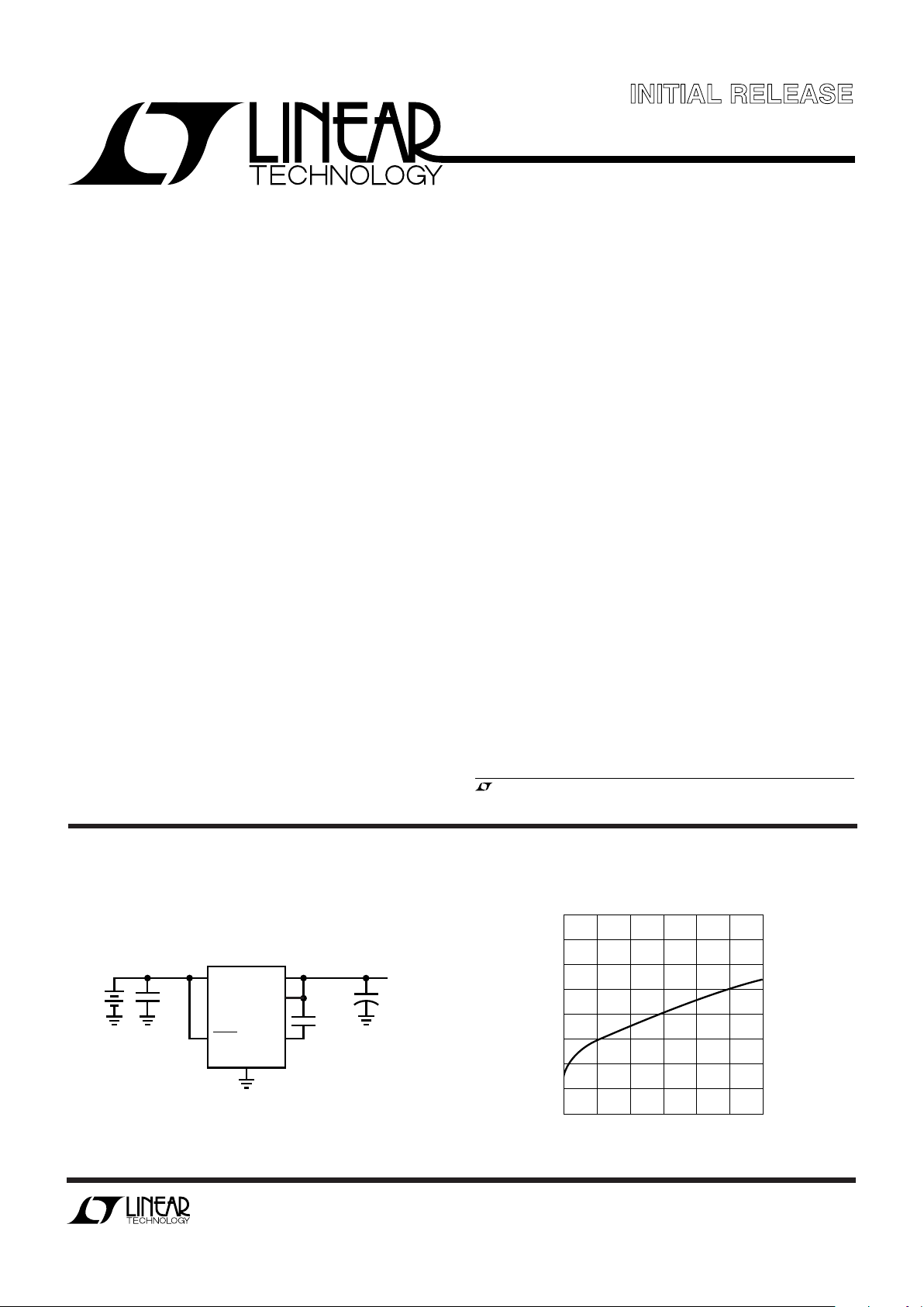
3.3V Low Noise Regulator
■
Cellular Phones
■
Battery-Powered Systems
■
Noise-Sensitive Instrumentation Systems
, LTC and LT are registered trademarks of Linear Technology Corporation.
IN
SHDN
0.01µF
10µF
1962 TA01
OUT
SENSE
V
IN
3.7V TO
20V
BYP
GND
LT1962-3.3
3.3V AT 300mA
20µV
RMS
NOISE
1µF
+
DESCRIPTIO
U
FEATURES
APPLICATIO S
U
TYPICAL APPLICATIO
U
Final Electrical Specifications
LOAD CURRENT (mA)
0
DROPOUT VOLTAGE (mV)
400
350
300
250
200
150
100
50
0
1962 TA02
100
200
30050
150
250
Dropout Voltage
Information furnished by Linear Technology Corporation is believed to be accurate and reliable.
However, no responsibility is assumed for its use. Linear Technology Corporation makes no representation that the interconnection of its circuits as described herein will not infringe on existing patent rights.
2
LT1962 Series
(Note 1)
IN Pin Voltage........................................................ ±20V
OUT Pin Voltage .................................................... ±20V
Input to Output Differential Voltage (Note 2) ......... ±20V
SENSE Pin Voltage ............................................... ±20V
ADJ Pin Voltage ...................................................... ±7V
BYP Pin Voltage....................................................±0.6V
SHDN Pin Voltage................................................. ±20V
Output Short-Circut Duration.......................... Indefinite
Operating Junction Temperature Range
(Note 3) ............................................ –40°C to 125°C
Storage Temperature Range ................. –65°C to 150°C
Lead Temperature (Soldering, 10 sec)..................300°C
Consult factory for Industrial and Military grade parts.
PARAMETER CONDITIONS MIN TYP MAX UNITS
Minimum Operating Voltage I
LOAD
= 300mA ● 1.8 2.3 V
Regulated Output Voltage LT1962-2.5 VIN = 3V, I
LOAD
= 1mA 2.475 2.500 2.525 V
(Note 5) 3.5V < V
IN
< 20V, 1mA < I
LOAD
< 300mA ● 2.435 2.500 2.565 V
LT1962-3 VIN = 3.5V, I
LOAD
= 1mA 2.970 3.000 3.030 V
4V < V
IN
< 20V, 1mA < I
LOAD
< 300mA ● 2.925 3.000 3.075 V
LT1962-3.3 VIN = 3.8V, I
LOAD
= 1mA 3.267 3.300 3.333 V
4.3V < V
IN
< 20V, 1mA < I
LOAD
< 300mA ● 3.220 3.300 3.380 V
LT1962-5 VIN = 5.5V, I
LOAD
= 1mA 4.950 5.000 5.050 V
6V < V
IN
< 20V, 1mA < I
LOAD
< 300mA ● 4.875 5.000 5.125 V
ADJ Pin Voltage LT1962 VIN = 2V, I
LOAD
= 1mA 1.208 1.220 1.232 V
(Notes 4, 5) 2.3V < V
IN
< 20V, 1mA < I
LOAD
< 300mA ● 1.190 1.220 1.250 V
Line Regulation LT1962-2.5 ∆VIN = 3V to 20V, I
LOAD
= 1mA ● 15 mV
LT1962-3 ∆V
IN
= 3.5V to 20V, I
LOAD
= 1mA ● 15 mV
LT1962-3.3 ∆V
IN
= 3.8V to 20V, I
LOAD
= 1mA ● 15 mV
LT1962-5 ∆V
IN
= 5.5V to 20V, I
LOAD
= 1mA ● 15 mV
LT1962 (Note 4) ∆V
IN
= 2V to 20V, I
LOAD
= 1mA ● 15 mV
Load Regulation LT1962-2.5 VIN = 3.5V, ∆I
LOAD
= 1mA to 300mA 5 12 mV
V
IN
= 3.5V, ∆I
LOAD
= 1mA to 300mA ● 25 mV
LT1962-3 VIN = 4V, ∆I
LOAD
= 1mA to 300mA 7 15 mV
V
IN
= 4V, ∆I
LOAD
= 1mA to 300mA ● 30 mV
LT1962-3.3 VIN = 4.3V, ∆I
LOAD
= 1mA to 300mA 7 17 mV
V
IN
= 4.3V, ∆I
LOAD
= 1mA to 300mA ● 33 mV
LT1962-5 VIN = 6V, ∆I
LOAD
= 1mA to 300mA 12 25 mV
V
IN
= 6V, ∆I
LOAD
= 1mA to 300mA ● 50 mV
LT1962 (Note 4) VIN = 2.3V, ∆I
LOAD
= 1mA to 300mA 2 6 mV
V
IN
= 2.3V, ∆I
LOAD
= 1mA to 300mA ● 12 mV
The ● denotes specifications which apply over the full operating temperature range, otherwise specifications are TA = 25°C. (Note 3)
ORDER PART
NUMBER
LT1962EMS8
LT1962EMS8-2.5
LT1962EMS8-3
LT1962EMS8-3.3
LT1962EMS8-5
MS8 PART MARKING
LTML
LTPT
LTPQ
LTPS
LTPR
T
JMAX
= 150°C, θJA = 125°C/W
SEE THE APPLICATIONS
INFORMATION SECTION
FOR ADDITIONAL
INFORMATION ON
THERMAL RESISTANCE
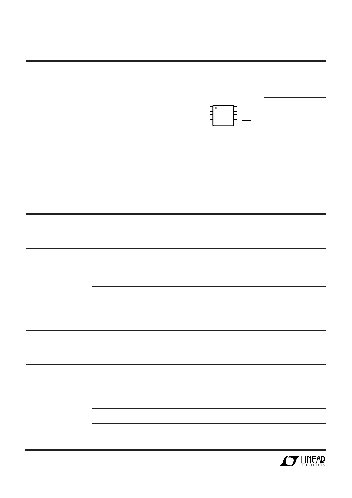
*PIN 2: SENSE FOR LT1962-2.5/LT1962-3/
LT1962-3.3/LT1962-5. ADJ FOR LT1962
1
2
3
4
OUT
SENSE/ADJ*
BYP
GND
8
7
6
5
IN
NC
NC
SHDN
TOP VIEW
MS8 PACKAGE
8-LEAD PLASTIC MSOP
ELECTRICAL CHARACTERISTICS
PACKAGE/ORDER I FOR ATIO
UU
W
ABSOLUTE AXI U RATI GS
WWWU
3
LT1962 Series
Dropout Voltage I
LOAD
= 10mA 0.10 0.15 V
V
IN
= V
OUT(NOMINAL)
I
LOAD
= 10mA ● 0.21 V
(Notes 6, 7)
I
LOAD
= 50mA 0.15 0.20 V
I
LOAD
= 50mA ● 0.28 V
I
LOAD
= 100mA 0.18 0.24 V
I
LOAD
= 100mA ● 0.33 V
I
LOAD
= 300mA 0.27 0.33 V
I
LOAD
= 300mA ● 0.43 V
GND Pin Current I
LOAD
= 0mA ● 30 75 µA
V
IN
= V
OUT(NOMINAL)
I
LOAD
= 1mA ● 65 120 µA
(Notes 6, 8)
I
LOAD
= 50mA ● 1.1 1.6 mA
I
LOAD
= 100mA ● 23 mA
I
LOAD
= 300mA ● 812 mA
Output Voltage Noise C
OUT
= 10µF, C
BYP
= 0.01µF, I
LOAD
= 300mA, BW = 10Hz to 100kHz 20 µV
RMS
ADJ Pin Bias Current (Notes 4, 9) 30 100 nA
Shutdown Threshold V
OUT
= Off to On ● 0.8 2 V
V
OUT
= On to Off ● 0.25 0.65 V
SHDN Pin Current V
SHDN
= 0V 0.01 0.5 µA
(Note 10) V
SHDN
= 20V 1 5 µA
Quiescent Current in Shutdown VIN = 6V, V
SHDN
= 0V 0.1 1 µA
Ripple Rejection VIN – V
OUT
= 1.5V (Avg), V
RIPPLE
= 0.5V
P-P
, f
RIPPLE
= 120Hz, 55 65 dB
I
LOAD
= 300mA
Current Limit VIN = 7V, V
OUT
= 0V 700 mA
V
IN
= V
OUT(NOMINAL)
+ 1V, ∆V
OUT
= –0.1V ● 320 mA
Input Reverse Leakage Current VIN = –20V, V
OUT
= 0V ● 1mA
Reverse Output Current LT1962-2.5 V
OUT
= 2.5V, VIN < 2.5V 10 20 µA
(Note 11) LT1962-3 V
OUT
= 3V, VIN < 3V 10 20 µA
LT1962-3.3 V
OUT
= 3.3V, VIN < 3.3V 10 20 µA
LT1962-5 V
OUT
= 5V, VIN < 5V 10 20 µA
LT1962 (Note 4) V
OUT
= 1.22V, VIN < 1.22V 5 10 µA
PARAMETER CONDITIONS MIN TYP MAX UNITS
The ● denotes specifications which apply over the full operating temperature range, otherwise specifications are TA = 25°C. (Note 2)
Note 6: To satisfy requirements for minimum input voltage, the LT1962
(adjustable version) is tested and specified for these conditions with an
external resistor divider (two 250k resistors) for an output voltage of
2.44V. The external resistor divider will add a 5µA DC load on the output.
Note 7: Dropout voltage is the minimum input to output voltage differential
needed to maintain regulation at a specified output current. In dropout, the
output voltage will be equal to: VIN – V
DROPOUT
.
Note 8: GND pin current is tested with VIN = V
OUT(NOMINAL)
and a current
source load. This means the device is tested while operating in its dropout
region. This is the worst-case GND pin current. The GND pin current will
decrease slightly at higher input voltages.
Note 9: ADJ pin bias current flows into the ADJ pin.
Note 10: SHDN pin current flows into the SHDN pin. This current is
included in the specification for GND pin current.
Note 11: Reverse output current is tested with the IN pin grounded and the
OUT pin forced to the rated output voltage. This current flows into the OUT
pin and out the GND pin.
Note 1: Absolute Maximum Ratings are those values beyond which the life
of a device may be impaired.
Note 2: Absolute maximum input to output differential voltage can not be
achieved with all combinations of rated IN pin and OUT pin voltages. With
the IN pin at 20V, the OUT pin may not be pulled below 0V. The total
measured voltage from in to out can not exceed ±20V.
Note 3: The LT1962 regulators are tested and specified under pulse load
conditions such that T
J
≈ TA. The LT1962 is 100% tested at TA = 25°C.
Performance at –40°C and 125°C is assured by design, characterization
and correlation with statistical process controls.
Note 4: The LT1962 (adjustable version) is tested and specified for these
conditions with the ADJ pin connected to the OUT pin.
Note 5: Operating conditions are limited by maximum junction
temperature. The regulated output voltage specification will not apply for
all possible combinations of input voltage and output current. When
operating at maximum input voltage, the output current range must be
limited. When operating at maximum output current, the input voltage
range must be limited.
ELECTRICAL CHARACTERISTICS
 Loading...