

Linear Technology LT1949 Datasheet
FEATURES
LT1949
600kHz, 1A Switch
PWM DC/DC Converter
U
DESCRIPTIO
■
1A, 0.5Ω, 30V Internal Switch
■
Operates with VIN as Low as 1.5V
■
600kHz Fixed Frequency Operation
■
Low-Battery Detector Stays Active in Shutdown
■
Low V
■
Pin-for-Pin Compatible with the LT1317B
■
Small 8-Lead MSOP and SO Packages
Switch: 410mV at 800mA
CESAT
U
APPLICATIO S
■
LCD Bias Supplies
■
GPS Receivers
■
Battery Backup
■
Portable Electronic Equipment
■
Diagnostic Medical Instrumentation
U
TYPICAL APPLICATIO
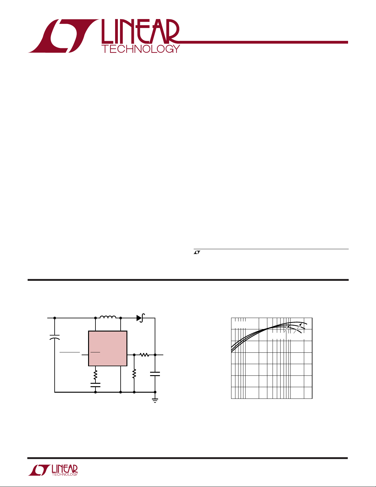
The LT®1949 is a fixed frequency step-up DC/DC converter with a 1A, 0.5Ω internal switch. Capable of generating 10V at 175mA from a 3.3V input, the LT1949 is ideal
for generating bias voltages for large screen LCD panels.
Constant frequency 600kHz operation results in a low
noise output that is easy to filter and the 30V switch rating
allows output voltage up to 28V using a single inductor. An
external compensation pin gives the user flexibility in
optimizing loop compensation, allowing small low ESR
ceramic capacitors to be used at the output. The 8-lead
MSOP and SO packages ensure a low profile overall
solution.
The LT1949 includes a low-battery detector that stays
alive when the device goes into shutdown. Quiescent
current in shutdown is 25µA, while operating current is
4.5mA.
, LTC and LT are registered trademarks of Linear Technology Corporation.
V
IN
3.3V
+
C1
22µF
C1: AVX TAJA226M006R
C2: TAIYO YUDEN LMK325BJ106MN
D1: MBRM120LT3
L1: SUMIDA CDRH62B-100
L1
10µH
V
IN
SHDNSHUTDOWN
V
C
68k
SW
LT1949
GND
330pF
D1
R1
FB
1M
R2
140k
V
OUT
10V
175mA
C2
10µF
CERAMIC
1949 F01
90
V
= 10V
OUT
80
70
60
50
EFFICIENCY (%)
40
30
20
5 10050 300
10
LOAD CURRENT (mA)
3.6V
4.2V
IN
IN
Figure 1. 3.3V to 10V/175mA DC/DC Converter Figure 2. 3.3V to 10V Converter Efficiency
3V
1949 F02
IN
1
LT1949
WWWU
ABSOLUTE AXI U RATI GS
(Note 1)
VIN, LBO Voltage..................................................... 12V
SW Voltage ............................................... –0.4V to 30V
FB Voltage .................................................... VIN + 0.3V
VC Voltage ................................................................ 2V
LBI Voltage ............................................ 0V ≤ V
LBI
≤ 1V
SHDN Voltage ........................................................... 6V
UU
W
PACKAGE/ORDER I FOR ATIO
ORDER PART
TOP VIEW
V
1
C
2
FB
3
SHDN
4
GND
MS8 PACKAGE
8-LEAD PLASTIC MSOP
T
= 125°C, θJA = 120°C/W
JMAX
Consult factory for Military grade parts.
8
LBO
7
LBI
6
V
IN
5
SW
NUMBER
LT1949EMS8
MS8 PART MARKING
LTJC
Junction Temperature.......................................... 125°C
Operating Temperature Range (Note 2)
LT1949EMS8.......................................–40°C to 85°C
LT1949ES8/LT1949IS8 .......................–40°C to 85°C
Storage Temperature ........................... – 65°C to 150°C
Lead Temperature (Soldering, 10sec).................. 300°C
ORDER PART
NUMBER
LT1949ES8
LT1949IS8
S8 PART MARKING
1949E
1949I
SHDN
GND
V
1
C
FB
2
3
4
T
JMAX
8-LEAD PLASTIC SO
TOP VIEW
8
7
6
5
S8 PACKAGE
= 125°C, θJA = 120°C/W
LBO
LBI
V
SW
IN
ELECTRICAL CHARACTERISTICS
temperature range, otherwise specifications are TA = 25°C. VIN = 2V, V
SYMBOL PARAMETER CONDITIONS MIN TYP MAX UNITS
I
V
I
g
A
f
Q
FB
B
m
V
OSC
Quiescent Current ● 4.5 7.5 mA
Feedback Voltage 1.22 1.24 1.26 V
FB Pin Bias Current (Note 3) ● 12 80 nA
Input Voltage Range ● 1.7 12 V
Error Amp Transconductance ∆I = 5µA ● 70 140 240 µmhos
Error Amp Voltage Gain 700 V/V
Maximum Duty Cycle ● 80 85 %
Switch Current Limit (Note 4) VIN = 2.5V, Duty Cycle = 30% 1 1.13 1.5 A
Switching Frequency ● 500 600 750 kHz
Shutdown Pin Current V
LBI Threshold Voltage 190 200 210 mV
LBO Output Low I
LBO Leakage Current V
LBI Input Bias Current (Note 5) V
Low-Battery Detector Gain 1MΩ Pull-Up 2000 V/V
Switch Leakage Current VSW = 5V ● 0.01 3 µA
The ● denotes specifications which apply over the full operating
= 2V unless otherwise noted.
SHDN
V
= 0V ● 25 40 µA
SHDN
● 1.20 1.24 1.26 V
V
= 2.5V, Duty Cycle = 30% ● 0.95 1.5 A
IN
= V
SHDN
IN
= 0V ● –2.3 – 7 µA
V
SHDN
= 10µA ● 0.15 0.25 V
SINK
= 250mV, V
LBI
= 150mV ● 560nA
LBI
= 5V ● 0.02 0.1 µA
LBO
● 0.015 0.1 µA
● 180 200 220 mV
2

LT1949
TEMPERATURE (°C)
–50
SWITCH CURRENT (A)
1.3
1.2
1.1
1.0
0.9
0.8
–25
02550
1949 G03
75 100
TEMPERATURE (°C)
–50 –25
QUIESCENT CURRENT (mA)
1949 G06
4.6
4.5
4.4
4.3
4.2
4.1
4.0
3.9
3.8
0 255075100
ELECTRICAL CHARACTERISTICS
temperature range, otherwise specifications are TA = 25°C. VIN = 2V, V
The ● denotes specifications which apply over the full operating
= 2V unless otherwise noted.
SHDN
SYMBOL PARAMETER CONDITIONS MIN TYP MAX UNITS
Switch V
CESAT
ISW = 800mA 410 mV
= 500mA ● 400 mV
I
SW
Reference Line Regulation 1.8V ≤ VIN ≤ 12V ● 0.08 0.15 %/V
SHDN Input Voltage High ● 1.4 6 V
SHDN Input Voltage Low ● 0.4 V
Note 1: Absolute Maximum Ratings are those values beyond which the life
of a device may be impaired.
Note 2: The LT1949E is guaranteed to meet performance specifications
from 0°C to 70°C. Specifications over the –40°C to 85°C operating
Note 3: Bias current flows into FB pin.
Note 4: Switch current limit guaranteed by design and/or correlation to
static tests. Duty cycle affects current limit due to ramp generator.
Note 5: Bias current flows out of LBI pin.
temperature range are assured by design, characterization and correlation
with statistical process controls.
UW
TYPICAL PERFOR A CE CHARACTERISTICS
Switch Current Limit,
Oscillator Frequency
700
Switch Current Limit
1.3
Duty Cycle = 30%
650
600
550
OSCILLATOR FREQUENCY (kHz)
500
0
Switch Voltage Drop (V
1.0
0.8
0.6
0.4
SWITCH VOLTAGE (V)
0.2
0
0
–40°C
25°C
85°C
2468
INPUT VOLTAGE
CESAT
25°C
–40°C
0.4 0.6 0.8
0.2
SWITCH CURRENT (A)
10 12
1949 G01
)
85°C
1.0 1.2
1949 G04
1.2
1.1
1.0
SWITCH CURRENT (A)
0.9
0.8
20
0
Feedback Voltage
1.25
1.24
1.23
1.22
FEEDBACK VOLTAGE (V)
1.21
1.20
–50
–25 0 25 50
60
40
DUTY CYCLE (%)
TEMPERATURE (°C)
80
1949 G02
75 100
1949 G05
100
Quiescent Current, SHDN = 2V
3
 Loading...