advertisement
Quad Output Switching Converter Provides Power
for Large TFT LCD Panels
– Design Note 349
Dongyan Zhou
Introduction
The LT®1943 is a highly integrated, 4-output regulator
designed to power large TFT LCD panels. The LT1943
employs switching regulators—instead of linear regulators—to minimize power dissipation and accommodate a
wide input voltage range. The wide input range, 4.5V to
22V, allows it to accept a variety of power sources,
including the commonly used 5V, 12V and 19V AC adaptors. The first buck regulator provides a logic voltage with
up to 2A of current. The other three switching regulators
provide the three bias voltages, AV
required by LCDs.
CMDSH-3
0.47µF
L1
4.7µH
0.22µF
V
OFF
–10V
50mA
V
LOGIC
3.3V
1.5A
2.2µF
10V
ZHCS400
ZHCS400
80.6k
10.0k
16.5k
10.0k
22µF
6.3V
DD
10pF
7.5k
100pF
, VON and V
4.5V TO 8V
10µF
10V
SW4
NFB4
FB4
BIAS
BOOST
SW1
FB1
VC1
100pF
V
4.7nF2.7nF
L3
10µH
B230A
,
OFF
IN
V
SW3
IN
LT1943
VC2 VC3 VC4
4.7k
All four regulators are synchronized to a 1.2MHz internal
clock, allowing the use of small, low cost inductors and
ceramic capacitors. Since different types of panels may
require different bias voltages, all output voltages are
adjustable for maximum flexibility. Programmable softstart capability is included in all outputs to limit inrush
current. The LT1943 has a built-in start-up sequence and
panel protection feature. The LT1943 is available in a lowprofile 28-pin TSSOP package.
, LTC and LT are registered trademarks of Linear Technology Corporation.
6.8µH
RUN-SS
SS-234
PGOOD
30k
100pF
1.5nF
L2
4.7µH
SW2
FB2
V
FB3
GND
SGND
C
T
ON
E3
0.015µF
13k
100pF
2.2nF
B240A
0.015µF
0.047µF
10µF
16V
95.3k 100k
10.0k
232k
10.0k
2.2µF
35V
AV
500mA
V
30V
20mA
0.47µF
35V
Si2343DS
DD
13V
ON
10/04/349
L1: TDK RLF7030T-4R7M3R4
L2: TDK SLF6028T-4R7M1R6
L3: TDK RLF5018T-100MR94
DN349 F01
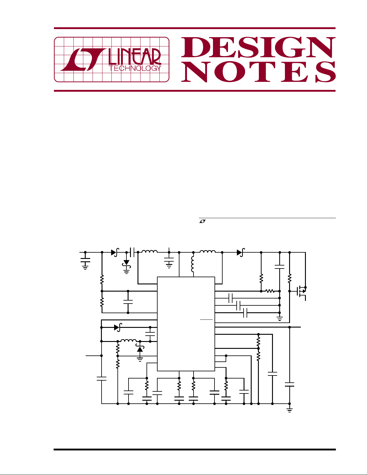
Figure 1. Quad Output TFT LCD Power Supply with 4.5V to 8V Input Voltage Range

4-Output Supply with Soft-Start
Figure 1 shows a 4-output TFT LCD power supply with a
4.5V to 8V input range. The first output provides a 3.3V,
up to 1.5A, logic supply using a buck regulator. The
second output employs a boost converter to generate a
13V, 500mA AV
and an inverter generate V
bias supply. Another boost converter
DD
and V
ON
OFF
.
When power is first applied to the input, the RUN/SS pin
starts charging. When its voltage reaches 0.7V, switcher 1
is enabled. The capacitor at RUN/SS pin controls the
V
ramping rate and inrush current in L1.
LOGIC
Switchers 2, 3 and 4 are controlled by the BIAS pin, which
is usually connected to V
. When the BIAS pin is
LOGIC
higher than 2.8V, the SS-234 pin begins charging to
enable switchers 2, 3 and 4. When AV
reaches approxi-
DD
mately 90% of its programmed voltage, the PGOOD pin is
pulled low. When AV
programmed voltages, the C
current source begins to charge C
reaches 1.1V, an output PNP turns on, enabling V
Since V
V
ON
has to be present to turn on the LCD panel, the
ON
turn-on delay gives the column drivers and digital
DD
, V
and E3 all reach 90% of their
OFF
timer is enabled and a 20µA
T
. When the CT pin
T
ON
.
circuitry in the LCD panel time to get ready, preventing
high currents from flowing into the panel.
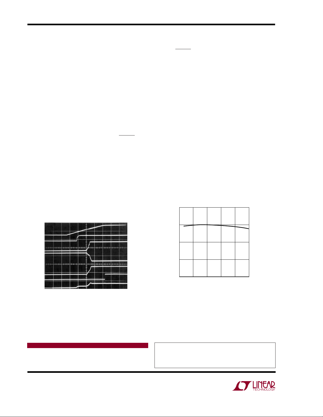
Figure 2 illustrates the start-up sequencing of the 4-output power
supply in Figure 1. Figure 3 gives the overall efficiency for
the circuit in Figure 1.
If one of the regulated voltages, V
LOGIC
, AVDD, V
OFF
or E3
drops more than 10%, the internal PNP turns off to shut
down VON. This action protects the panel in a fault condition. The PGOOD pin is used to drive an optional PMOS
device at the output of the AV
disconnect AV
from the input during shutdown.
DD
boost regulator to
DD
The converter uses all ceramic capacitors. X5R or X7R
type ceramic capacitors are recommended, as these
materials retain their capacitance over a wide temperature
range.
Wide Input Range Supply
If the input voltage may be higher than the AVDD set value,
a SEPIC regulator can be used in place of a boost regulator
to generate the AV
output. This covers the commonly
DD
used 12V and 19V inputs. Details for this are covered in
the LT1943 data sheet.
Conclusion
The LT1943 simplifies and shrinks power supplies for TFT
LCD panels. Its four integrated switching regulators enable a wide input voltage range and reduce power dissipation. All regulators have a 1.2MHz switching frequency
and allow the exclusive use of ceramic capacitors to
minimize circuit size, cost and output ripple.
100
RUN-SS
2V/DIV
V
LOGIC
5V/DIV
AV
DD
10V/DIV
V
OFF
10V/DIV
V
E3
20V/DIV
V
ON
50V/DIV
I
IN(AVG)
1A/DIV
Figure 2. Start-Up Waveforms of the
Power Supply in Figure 1
Data Sheet Download
http://www.linear.com
5ms/DIV
DN349 F02
90
80
EFFICIENCY (%)
70
60
300
0
LOAD AT V
600
900
LOGIC
(A)
1200
1500
DN349 F03
Figure 3. Total Circuit Efficiency of the Power
Supply in Figure 1 (Load at AVDD: 500mA)
For applications help,
call (408) 432-1900, Ext. 3531
Linear Technology Corporation
1630 McCarthy Blvd., Milpitas, CA 95035-7417
(408) 432-1900 ● FAX: (408) 434-0507 ● www.linear.com
dn349f LT/TP 1004 305K • PRINTED IN THE USA
© LINEAR TECHNOLOGY CORPORATION 2004
 Loading...