

FEATURES
■
Triple Output TFT Supply with Built-In
Power Sequencing
■
Integrated White LED Backlight Driver
■
Integrated Schottky Diodes
■
Active Ballast Circuitry Ensures Precise Current
Matching in White LEDs
■
Low Noise 1MHz Fixed Frequency Operation
■
2.6V to 16V Input Voltage Range
■
Soft-Start Limits Inrush Current
■
TFT Supply Output Voltages Independently Set
(Not Charge Pump Derived)
■
Power Good and Output Disconnect for TFT Supply
■
Built-In LED Dimming Capability
■
Open LED Protection for LED Driver
■
24-Lead QFN Package (4mm × 4mm)
U
APPLICATIO S
■
Poly-Silicon TFT Displays
■
Amorphous Silicon TFT Displays
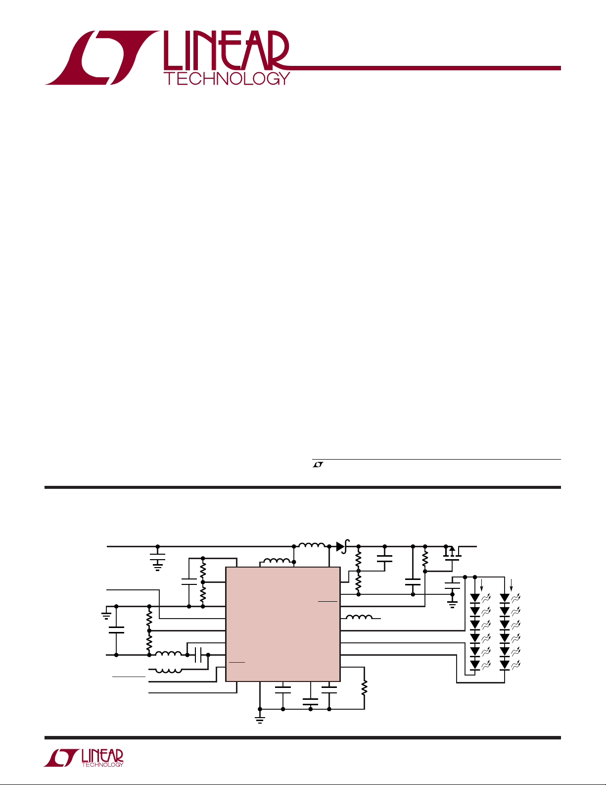
LT1942
Quad DC/DC Converter
for Triple Output TFT Supply
Plus LED Driver
U
DESCRIPTIO
The LT®1942 is a highly integrated quad switching regulator designed to provide all necessary power supply
functions for TFT displays, including the white LED
backlight driver. The TFT supply incorporates two boost
and one inverting DC/DC converters. The TFT supply
output voltages are independently set, unlike charge
pump solutions which have many limitations. Power
sequencing for the TFT supply is built into the part and is
user programmable.
The LED driver is a boost DC/DC converter that can be
independently controlled. The LED driver has built-in
dimming control for precise control of LED current. An 8:1
dimming range is achieved by adjusting the CTRL4
voltage.The user can elect to drive a single string or two
strings of LEDs. An LED ballast circuit is included to
precisely match the LED currents if two strings of LEDs are
used. Soft-start is built into the LED driver as well as the
primary TFT supply.
The LT1942 is available in a low profile (0.75mm) 24-lead
QFN (4mm × 4mm) package.
, LTC and LT are registered trademarks of Linear Technology Corporation.
All other trademarks are the property of their respective owners.
V
3V TO 4.2V
V
10V
2mA
V
OFF
–10V
2mA
IN
ON
SHUTDOWN
LED CONTROL
10k
0.22µF
665k
TFT Bias and White LED Backlight Power Supply
CMDSH-3
22µH
0.22µF
698k
100k
0.1µF
D3 SW3
FB3
PGND23
V
OUT3
NFB2
D2
SW2
SHDN
CTRL4
0.22µF
47µH
47µH
V
IN
22µH
SGND/
AGND
V
CC
PGND14
LT1942
SS1 SS4 CT
0.1µF
SW1
FB1
PGOOD
SW4
LED1
LED2
FB4
4.99Ω
V
4.7pF
4.7µF
IN
301k
100k
33µH
D4
0.1µF0.1µF
Si2301BDS
1M
4.7µF
AV
DD
5V
40mA
20mA 20mA
1942 TA01
1942fa
1
LT1942
PACKAGE/ORDER I FOR ATIO
UU
W
WWWU
ABSOLUTE AXI U RATI GS
(Note 1)
VCC Voltage............................................................. 16V
SW1, SW2, SW3 Voltage .......................... –0.4V to 36V
SW4.......................................................... –0.4V to 45V
FB1, FB3 Voltage ................................................... 2.5V
FB4 Voltage ....................................................... 400mV
NFB2 Voltage ................................................... –200mV
SHDN Voltage ......................................................... 10V
CTRL4 Voltage ........................................................ 16V
SS1, SS4 Voltage .................................................. 1.5V
Current Into D2 ......................................................... 1A
D2 Voltage ............................................................ –36V
Current Out of D3 ..................................................... 1A
D3 Voltage .............................................................. 36V
Current Out of D4 ..................................................... 4A
D4 Voltage .............................................................. 45V
LED1, LED2 Voltage ............................................... 45V
Current Into LED1, LED2 ..................................... 35mA
PGOOD Voltage ...................................................... 16V
V
Voltage ......................................................... 36V
OUT3
CT Current ........................................................... ±1mA
Maximum Junction Temperature ......................... 125°C
Operating Temperature Range (Note 2) .. – 40°C to 85°C
Storage Temperature Range ................ –65°C to 125°C
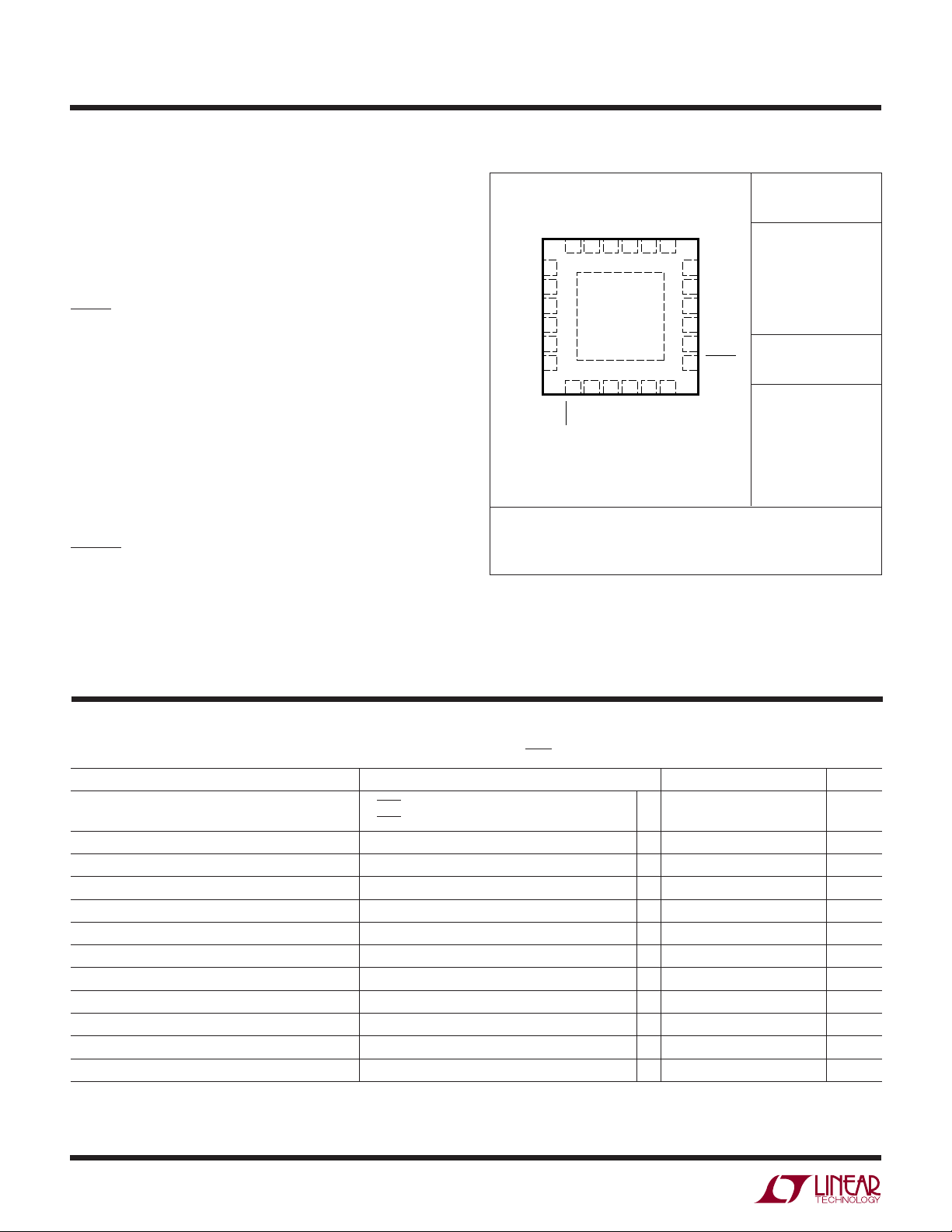
TOP VIEW
ORDER PART
NUMBER
SW2D2VCCPGND14
24 23 22 21 20 19
PGND23
1
SW3
2
D3
3
V
4
OUT3
FB3
5
NFB2
6
7 8 9
SHDN
CTRL4
24-LEAD (4mm × 4mm) PLASTIC QFN
T
JMAX
Order Options Tape and Reel: Add #TR
Lead Free: Add #PBF Lead Free Tape and Reel: Add #TRPBF
Lead Free Part Marking: http://www.linear.com/leadfree/
Consult LTC Marketing for parts specified with wider operating temperature ranges.
UF PACKAGE
= 125°C, θJA = 37°C/W, θJC = 4.3°C/W
EXPOSED PAD (PIN 25) IS SGND
(MUST BE SOLDERED TO PCB)
25
10 11 12
CT
AGND
SW1
SS1
SW4
SS4
LT1942EUF
18
LED1
LED2
17
D4
16
FB4
15
FB1
14
13
PGOOD
UF PART
MARKING
1942
ELECTRICAL CHARACTERISTICS
temperature range, otherwise specifications are at T
PARAMETER CONDITIONS MIN TYP MAX UNITS
Quiescent Current V
Input Voltage Range VCC Pin
AVDD Feedback Voltage FB1 Pin
AVDD Feedback Pin Bias Current (FB1) FB1 Pin (Note 3) 15 60 nA
AVDD Feedback Voltage for Power Good Signal FB1 Pin Voltage as a Percent of Nominal Voltage
V
Feedback Voltage NFB2 Pin –160 –150 –140 mV
OFF
V
Feedback Pin Bias Current (NFB2) NFB2 Pin (Note 3) 25 60 nA
OFF
VON Feedback Voltage FB3 Pin 1.225 1.25 1.275 V
VON Feedback Pin Bias Current (FB3) FB3 Pin (Note 3) 25 60 nA
LED Feedback Voltage FB4 Pin, V
LED Feedback Pin Bias Current (FB4) FB4 Pin (Note 3) 20 60 µA
LED Feedback Voltage with Dimming FB4 Pin, V
V
SHDN
SHDN
The ● denotes the specifications which apply over the full operating
= 25°C. VIN = 3.3V, V
A
= 3.3V, V
= V
CTRL4
CTRL4
CTRL4
= 0V, Not Switching
CTRL4
= 0V, In Shutdown
= 3.3V
= 1V 85 95 105 mV
= VIN, unless otherwise noted. (Note 2)
SHDN
●
●
●
2.6 16 V
●
1.225 1.25 1.275 V
●
95 97 100 %
●
190 200 210 mV
710 mA
01 µA
1942fa
2
LT1942
ELECTRICAL CHARACTERISTICS
temperature range, otherwise specifications are at T
The ● denotes the specifications which apply over the full operating
= 25°C. VIN = 3.3V, V
A
= VIN, unless otherwise noted. (Note 2)
SHDN
PARAMETER CONDITIONS MIN TYP MAX UNITS
LED1-LED2 Current Matching Current Into Each Pin = 20mA, V
Current Into Each Pin = 20mA, |V
LED1 Voltage 20mA Into Pin, V
LED2 Voltage 20mA Into Pin, V
LED1, LED2 Maximum Current Into Either Pin, V
LED1, LED2 Leakage Current V
SHDN
= 0V, V
= 2V, FB4 = 0 1 1.2 V
LED2
= 2V, FB4 = 0 1 1.2 V
LED1
< 1.5V, FB4 = 0 35 mA
LEDX
= 45V
LEDX
= V
LED1
LED1-VLED2
LED2
0 1.5 %
| = 1V 1 2.5 %
●
1 µA
AVDD Maximum Duty Cycle SW1 Pin 88 93 %
V
Maximum Duty Cycle SW2 Pin 75 86 %
OFF
VON Maximum Duty Cycle SW3 Pin 75 86 %
LED Maximum Duty Cycle SW4 Pin 88 93 %
AVDD Switch Current Limit at Minimum DC (SW1) SW1 Pin (Note 4) 150 200 250 mA
AVDD Switch Current Limit at Maximum DC (SW1) SW1 Pin (Note 4) 80 140 200 mA
V
Switch Current Limit at Minimum DC (SW2) SW2 Pin (Note 4) 50 80 110 mA
OFF
V
Switch Current Limit at Maximum DC (SW2) SW2 Pin (Note 4) 30 60 90 mA
OFF
VON Switch Current Limit at Minimum DC (SW3) SW3 Pin (Note 4) 50 80 110 mA
VON Switch Current Limit at Maximum DC (SW3) SW3 Pin (Note 4) 30 60 90 mA
LED Switch Current Limit at Minimum DC (SW4) SW4 Pin (Note 4) 550 750 900 mA
LED Switch Current Limit at Maximum DC (SW4) SW4 Pin (Note 4) 450 600 850 mA
V
Schottky Diode Forward Drop D2 Pin, I = 60mA 0.65 V
OFF
V
Schottky Diode Leakage Current D2 Pin, VD2 = –36V
OFF
●
1 µA
VON Schottky Diode Forward Drop D3 Pin, I = 60mA 0.65 V
VON Schottky Diode Leakage Current VD3 = 36V, SW3 = 0V, Output Disconnect PNP Off
●
1 µA
LED Schottky Diode Forward Drop I = 250mA 0.75 V
LED Schottky Diode Leakage Current VD4 = 36V, SW4 = 0V
●
1 µA
Switching Frequency 0.8 1 1.2 MHz
SHDN Pin Current V
CTRL4 Pin Current V
SW1-SW4 leakage Current V
SW1 V
CESAT
SW2 V
CESAT
SW3 V
CESAT
SW4 V
CESAT
= 3V
SHDN
= 0V 20 30 nA
V
SHDN
= 3V
CTRL4
V
= 0V –60 –150 nA
CTRL4
= 36V
SWX
I
= 100mA (Note 5) 200 300 mV
SW1
I
= 40mA (Note 5) 150 250 mV
SW2
I
= 40mA (Note 5) 150 250 mV
SW3
I
= 400mA (Note 5) 280 400 mV
SW4
●
●
●
70 100 µA
30 60 µA
0.01 1 µA
SS1 Charging Current VSS = 0.5V 1 3 5 µA
SS4 Charging Current VSS = 0.5V 1 3 5 µA
SHDN Input Voltage High 1V
SHDN Input Voltage Low 0.4 V
CTRL4 Input Voltage High 0.25 V
CTRL4 Input Voltage Low 0.1 V
1942fa
3
LT1942
TEMPERATURE (°C)
–40
VOLTAGE (V)
1.26
1.27
1.28
20 60
1942 G01
1.25
1.24
–20 0
40 80 100
1.23
1.22
ELECTRICAL CHARACTERISTICS
temperature range, otherwise specifications are at T
The ● denotes the specifications which apply over the full operating
= 25°C. VIN = 3.3V, V
A
= VIN, unless otherwise noted. (Note 2)
SHDN
PARAMETER CONDITIONS MIN TYP MAX UNITS
PGOOD Leakage Current PGOOD NPN Off, V
PGOOD Sink Current PGOOD NPN On, V
= 5V 0 0.1 µA
PGOOD
= 1V 0.5 0.7 mA
PGOOD
CT Charging Current 12 µA
CT Reference Voltage 0.8 V
V
Leakage Current Output Disconnect PNP Off, D3 = 36V, V
OUT3
V
Source Current Output Disconnect PNP On, D3 = 3V, V
OUT3
Minimum D3/V
Operating Voltage Minimum D3 Voltage for Proper Output 3 V
OUT3
= 0V 0 1 µA
OUT
= 2.5V 10 15 mA
OUT
Disconnect PNP Operation
D4 LED Open-Circuit Voltage 38 42 44 V
Note 1: Absolute Maximum Ratings are those values beyond which the life
of a device may be impaired.
Note 2: The LT1942 is guaranteed to meet performance specifications
from 0°C to 70°C. Specifications over the –40°C to 85°C operating
Note 3: Current flows out of the pin.
Note 4: Current limit guaranteed by design and/or correlation to static test.
Note 5: V
100% tested at wafer level.
CESAT
temperature range are assured by design, characterization and correlation
with statistical controls.
UW
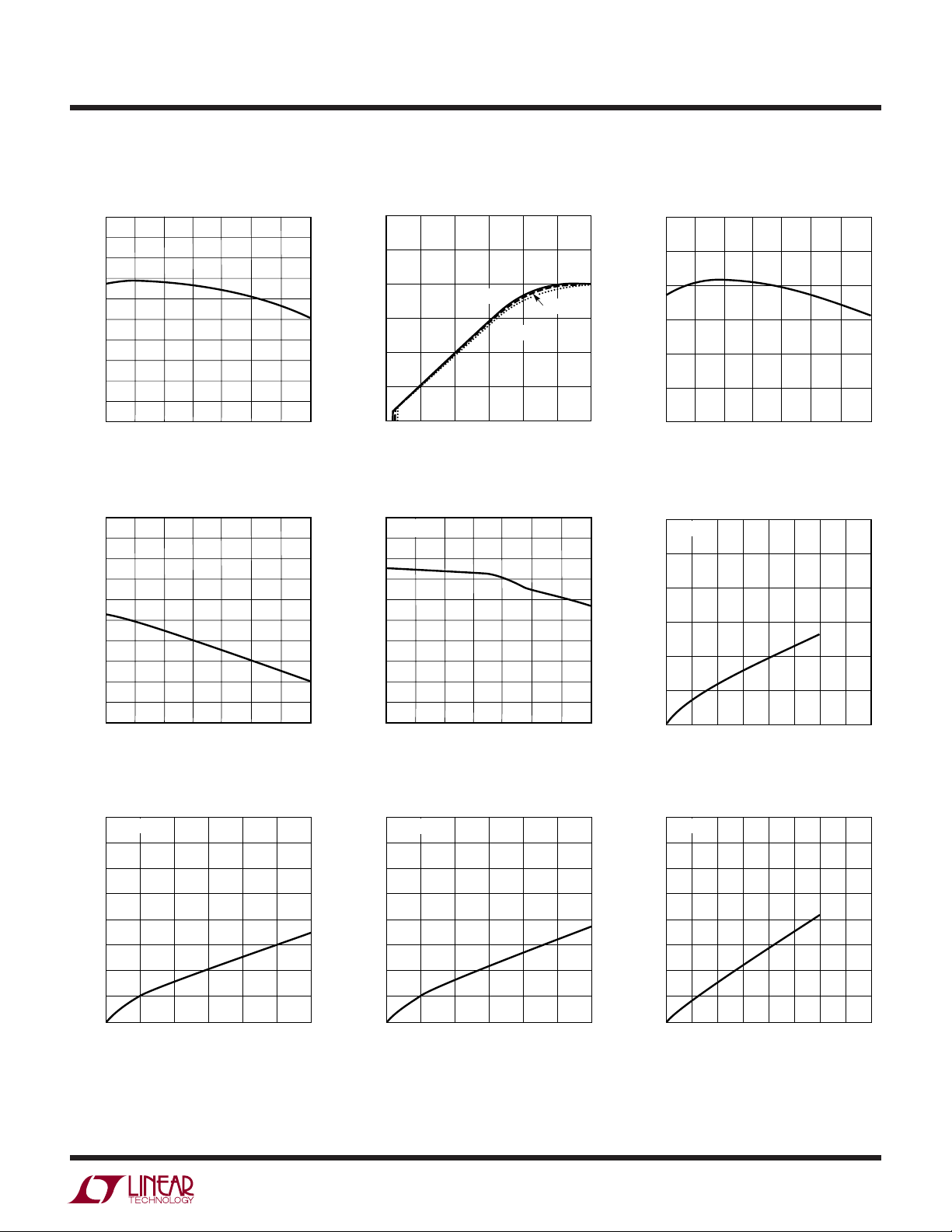
TYPICAL PERFOR A CE CHARACTERISTICS
V
FB1
1.28
1.27
1.26
1.25
VOLTAGE (V)
1.24
1.23
1.22
–40
Voltage
–20 0
40 80 100
20 60
TEMPERATURE (°C)
1942 G01
NFB2 Voltage V
–145
–146
–147
–148
–149
–150
–151
VOLTAGE (mV)
–152
–153
–154
–155
–40
–20
0
40
20
TEMPERATURE (°C)
60
80
100
1942 G02
Voltage
FB3
4
1942fa
UW
TEMPERATURE (°C)
–40
OSCILLATOR FREQUENCY (kHz)
1000
1100
1200
20 60
1942 G06
900
800
–20 0
40 80 100
700
600
SW1 CURRENT (mA)
0
0
SW1 SATURATION VOLTAGE (mV)
100
200
300
400
50
100
200150 175
1942 G09
500
600
25
75
125
TA = 25°C
SW4 CURRENT (mA)
0
SW4 SATURATION VOLTAGE (mV)
300
400
500
300
700
1942 G12
200
100
0
100 200 500
600
400
600
700
800
800
TA = 25°C
TYPICAL PERFOR A CE CHARACTERISTICS
LT1942
FB4 Voltage V
210
208
206
204
202
(mV)
200
FB4
V
198
196
194
192
190
–40
–20
0
40
20
TEMPERATURE (°C)
60
80
100
1942 G04
300
250
200
(mV)
150
FB4
V
100
vs CTRL4 Oscillator Frequency
FB4
TA = –40°C
T
A
50
0
0
0.5
1 1.5 2
CTRL4 (V)
TA = 25°C
= 85°C
2.5 3
1942 G05
Quiescent Current CT Timer Delay Time SW1 Saturation Voltage
10.0
9.5
9.0
8.5
8.0
7.5
7.0
6.5
QUIESCENT CURRENT (mA)
6.0
5.5
5.0
–40
–20
0
TEMPERATURE (°C)
40
20
60
80
100
1942 G07
10
CT = 0.1µF
9
8
7
6
5
4
DELAY TIME (ms)
3
2
1
0
–40
–20
40
20
0
TEMPERATURE (°C)
80
100
1942 G08
60
400
TA = 25°C
350
300
250
200
150
100
SW2 SATURATION VOLTAGE (mV)
50
0
10 20 40
0
30
SW2 CURRENT (mA)
SW3 Saturation VoltageSW2 Saturation Voltage SW4 Saturation Voltage
400
TA = 25°C
350
300
250
200
150
100
SW3 SATURATION VOLTAGE (mV)
50
0
10 20 40
50
60
1942 G10
0
30
SW3 CURRENT (mA)
50
60
1942 G10
1942fa
5

LT1942
UW
TYPICAL PERFOR A CE CHARACTERISTICS
LED1 to LED2 Current Matching V
2.0
V
= V
LED1
1.5
1.0
0.5
0
–0.5
–1.0
–1.5
LED1 CURRENT MATCHING ERROR (%)
–2.0
2 6 10 14 18 26 30
+ 1V
LED2
LED2 CURRENT (mA)
TA = 85°C
TA = 25°C
TA = –40°C
22
34
1942 G13
D4 Forward Voltage V
1400
TA = 25°C
1200
500
450
400
350
300
250
200
VOLTAGE DROP (mV)
150
OUT3
100
D3-V
50
1400
1200
vs I
0
0.01
TA = 25°C
OUT3
OFF
OUT3
TA = 85°C
0.1 1 10
I
CURRENT (mA)
OUT3
Diode Forward Voltage
TA = 25°C
TA = –40°C
1942 G14
LED Open-Circuit Protection
Voltage
44.0
43.8
43.6
43.4
43.2
43.0
VOLTAGE (V)
42.8
OUT4
V
42.6
42.4
42.2
42.0
1400
1200
–40
–20
V
Diode Forward Voltage
ON
TA = 25°C
20
0
TEMPERATURE (°C)
40
60
80
100
1942 G08
1000
800
600
400
D4 FORWARD VOLTAGE (mV)
200
0
0.1 10 100 1000
1
D4 CURRENT (mA)
300
250
200
(mA)
150
LIM
I
100
50
0
20
AV
Switcher Current Limit
DD
TA = 25°C
30 40
1942 G16
60 80 90
50 70
DUTY CYCLE (%)
1000
800
600
400
DIODE FORWARD VOLTAGE (mV)
200
OFF
V
0
0.1 10 100 1000
1942 G18
1
V
DIODE CURRENT (mA)
OFF
900
800
700
600
500
(mA)
400
LIM
I
300
200
100
1000
800
600
400
DIODE FORWARD VOLTAGE (mV)
200
ON
V
0
0.1 10 100 1000
1942 G17
LED Switcher Current Limit
TA = 25°C
0
20
30
40
50 90
DUTY CYCLE (%)
60
1
VON DIODE CURRENT (mA)
1942 G19
70 80
1942 G20
6
1942fa

LT1942
U
UU
PI FU CTIO S
PGND23 (Pin 1): Power Ground for V
Tie directly to local ground plane.
SW3 (Pin 2): Switch Pin for V
ON
collector of an internal NPN power switch. Minimize the
metal trace area connected to this pin to minimize EMI.
D3 (Pin 3): Output of V
Switcher. Place output decoup-
ON
ling capacitor from this pin to local ground plane.
V
(Pin 4): Collector of Internal Output Disconnect
OUT3
PNP Transistor for the V
Switcher. Place a capacitor
ON
from this pin to local ground plane of at least 0.1µF.
FB3 (Pin 5): Feedback Pin for VON Switcher. Reference
voltage is 1.25V. Connect resistive divider tap here.
Minimize trace area at FB3. Set V
= 1.25(1 + R5/R6).
NFB2 (Pin 6): Feedback Pin for V
voltage is –150mV. Connect resistive divider tap here.
Minimize trace area at NFB2. Set V
V
= (–0.15)(1 + R3/R4).
OUT2
SHDN (Pin 7): Shutdown. Tie to 1V or greater to enable the
part. Tie to 0.4V or lower to disable. This pin is the global
shutdown pin for all four switching regulators.
and VON Switcher.
OFF
Switcher. This is the
according to V
OUT3
Switcher. Reference
OFF
according to
OUT2
OUT3
AGND (Pin 10): Analog Ground. Tie directly to local
ground plane.
SS1 (Pin 11): Soft-Start Pin for AV
Switcher. Place a
DD
soft-start capacitor from this pin to ground. Upon start-up,
3µA of current charges the capacitor to 1.25V. Use larger
capacitor for slower start-up. Leave floating if not in use.
SS4 (Pin 12): Soft-Start for LED Switcher. Place a softstart capacitor from this pin to ground. Upon start-up, 3µA
of current charges the capacitor to 1.25V. Use larger
capacitor for slower start-up. Leave floating if not in use.
PGOOD (Pin 13): Power Good Indication for AV
Open-collector NPN. Stays open until the V
Switcher.
DD
voltage
FB1
reaches 97% of target value at which point the pin will pull
down.
FB1 (Pin 14): Feedback Pin for AVDD Switcher. Connect
resistive divider tap here. Minimize trace area at FB1. Set
according to V
V
OUT1
= 1.25(1 + R1/R2).
OUT1
FB4 (Pin 15): Feedback Pin for LED Switcher. Place a
resistor from this node to ground. Choose R7 to set LED
current (I
if V
) according to the following formula:
LED
≥ 2.5V, R7 = 0.2/I
CTRL4
LED
CTRL4 (Pin 8): Shutdown for the LED Switcher. Tie to
0.25V or greater to enable the LED switcher. Tie to 0.1V or
lower to disable. CTRL4 can also override the default 200mV
reference for the LED switcher. If CTRL4 is tied to 2.5V or
greater, the reference voltage is 200mV. If CTRL4 is less
than 2.5V, the LED reference voltage is approximately
/10. This allows an 8:1 dimming range for the LEDs.
V
CTRL4
Refer to the Applications Section for more information.
CT (Pin 9): Programmable Delay for the TFT Supplies.
Place a capacitor from this pin to local ground plane. After
the delay, the output disconnect PNP for the V
turned on. The delay time is initiated when AV
supply is
ON
reaches
DD
97% of its final value.
In this case, I
LEDs are used, I
strings. If only a single string of LEDs is used, I
is the total LED current. If two strings of
LED
is the sum of the current in the two
LED
LED
is
simply the single string current. For dimming LED current,
drive V
to a lower voltage. See the Applications
CTRL4
Section for more information.
D4 (Pin 16): Output of LED Switcher. Place output decoupling capacitor from this pin to local ground plane.
LED2 (Pin 17): Second Input of Current Mirror for an LED
String. Connect the negative end of second string of LEDs
to this pin. If not in use, leave floating.
1942fa
7

LT1942
U
UU
PI FU CTIO S
LED1 (Pin 18): First Input of Current Mirror for an LED
String. Connect the negative end of first string of LEDs to
this pin. If not in use, leave floating.
SW4 (Pin 19): Switch Pin for LED Switcher. This is the
collector of an internal NPN power switch. Minimize the
metal trace area connected to this pin to minimize EMI.
SW1 (Pin 20): Switch Pin for AVDD Switcher. This is the
collector of an internal NPN Power switch. Minimize the
metal trace area connected to this pin to minimize EMI.
PGND14 (Pin 21): Power Ground for LED Switcher and
Switcher. Tie directly to local ground plane.
AV
DD
V
(Pin 22): Input Supply. Must be locally bypassed.
CC
D2 (Pin 23): Anode Connection of Internal Schottky Diode
for V
SW2 (Pin 24): Switch Pin for V
collector of an internal NPN Power switch. Minimize the
metal trace area connected to this pin to minimize EMI.
SGND (Pin 25): Signal Ground. This is the Exposed Pad,
which must be soldered directly to a local ground plane to
achieve optimum thermal performance.
Switcher.
OFF
Switcher. This is the
OFF
8
1942fa

BLOCK DIAGRA
LT1942
W
SHDN
7
V
CC
22
ONE
SHOT
PGOOD
13
QS
R
ENABLE
1MHz
OSCILLATOR
ENABLE
FB1
14
–150mV
REFERENCE
NFB2
1.250V
REFERENCE
ENABLE
1.250V
REFERENCE
+
–
6
FB3
5
SS1
11
SOFT-START
+
COMPARATOR
–
AV
BOOST CONVERTER
DD
RQ
DRIVER
S
SW1
20
Q1
+
–
Σ
+
28mV
–
–
+
RAMP-PULSE
GENERATOR
V
OFF
COMPARATOR
–
INVERTING CONVERTER
RQ
S
DRIVER
+
–
PGND14
SW2
24
Q2
+
+
Σ
RAMP-PULSE
GENERATOR
V
BOOST CONVERTER
ON
+
COMPARATOR
–
–
RQ
S
–
SW3
2
DRIVER
Q3
+
D2
D2
23
D3
3
D3
Q5
V
OUT3
4
+
Σ
–
PNP
DRIVE
CTRL4
8
AGND
10
200mV
ENABLE
90k
10k
FB4
SS4
12
+
–
SOFT-START
RAMP-PULSE
GENERATOR
Σ
RAMP-PULSE
GENERATOR
COMPARATOR
–
+
40V
LED BOOST CONVERTER
RQ
S
DRIVER
LED1
18
CT
9
LED2
17
SW4
19
D4
16
DELAY
GENERATOR
1
PGND23
D4
Q4
+
Q6
–
21
1942BD
PGND14
15
FB4
Q7
1942fa
9

LT1942
OPERATIO
U
Refer to the figure on the first page of this data sheet and
the Block Diagram when following the description of the
operation of the LT1942. The LT1942 contains four switching regulators. Three switchers are designed to be used as
the power supply for driving small to medium sized TFT
displays. The fourth switcher is designed to power an LED
backlight. All four switching regulators use a constant
frequency, current mode control scheme to provide excellent line and load regulation.
TFT Supply
The three switching regulators for the TFT supply are
named AV
switchers are boost type, while the V
type. Power sequencing circuitry is integrated into the
LT1942 to properly power up the TFT power supply. When
the SHDN pin is driven above 1V initially, only the AV
switcher is enabled. After the output of the AVDD switcher
reaches 97% of its final value, the PGOOD pin is driven low
and both the V
event is latched rejecting any later drops on AV
97%. The output-disconnect circuitry (Q5 in the Block
Diagram) for the V
programmable delay set by the CT pin has elapsed. Once
the output-disconnect circuitry is enabled, the V
driven to nearly the same voltage as D3. The V
only source current and is limited to 15mA nominally. All
three switching regulators are internally compensated and
operated at a fixed frequency of 1MHz. The AVDD switching regulator has integrated soft-start. Simply place a
capacitor from the SS1 pin to GND to implement soft-start.
DD
, V
and VON. Both the AVDD and V
OFF
is an inverting
OFF
and VON switchers are enabled. This
OFF
switcher is not activated until the
ON
OUT3
below
DD
OUT3
pin can
ON
DD
pin is
LED Supply
The fourth switching regulator in the LT1942 is designed
to drive up to 20 LEDs (2 strings of 10) to power a
backlight. The LED switcher has an integrated current
ballaster (Q6 and Q7 in the Block Diagram) which enables
two strings of LEDs to have active current matching. The
current into LED1 and LED2 will always be actively matched,
regardless of which LED string has the highest voltage
drop. The LED ballast circuitry can be left unused when
driving a single string of LEDs. Simply leave the LED1 and
LED2 inputs floating and return the LED string directly to
the FB4 pin. The LED switcher has an independent control
pin which serves two functions: shutdown and reference
adjustment. The CTRL4 pin needs to be driven above
0.25V to enable the LED switcher. When CTRL4 is between
0.25V and 2.5V, the internal reference for the LED switcher
is attenuated. If CTRL4 is above 2.5V, the internal reference is limited to 200mV no matter how high CTRL4 is.
This feature allows an 8:1 dimming range for the LEDs.
The LED switching regulator is internally compensated
and operates at a fixed frequency of 1MHz. The LED
switching regulator has LED open-circuit protection. If
any LED fails open, D4 is not allowed to exceed 42V
(typical). This prevents damage to the power switch. The
LED switching regulator also has built in soft-start. By
placing a capacitor from the SS4 pin to GND, the user can
program the soft-start time.
10
1942fa

WUUU
APPLICATIO S I FOR ATIO
LT1942
Setting the Output Voltages
Unlike charge-pump-based TFT supplies, the LT1942 TFT
, V
outputs can all be independently set. The AV
V
outputs are all inductively based DC/DC converters.
ON
DD
OFF
and
As such, the output voltages are set by choosing the right
feedback divider ratio. The AV
the reference voltage is 1.25V. The V
NFB2 and the reference voltage is –150mV. The V
feedback pin is FB1 and
DD
feedback pin is
OFF
ON
feedback pin is FB3 and the reference voltage is 1.25V. The
LED driver is also an inductively based DC/DC converter.
Output Disconnect
The V
nect. When the V
switching regulator has built in output discon-
ON
supply is enabled, the boost converter
ON
will charge up the D3 node. With the output disconnect
PNP (Q5) turned off, the voltage on V
will be zero.
OUT3
Once the power sequencing circuitry turns on the PNP,
will go to nearly the same voltage as D3.
V
OUT3
The V
switching regulator naturally achieves output
OFF
disconnect due to the switching topology (inverting configuration). When the LT1942 is in shutdown, V
OFF
will go
to zero volts.
latches low turning on the PMOS device and bringing the
output quickly to the desired voltage.
AV
DD
Soft-Start
The higher current regulators, AV
and LED, have user
DD
programmable soft-start functions built into the part.
Simply place a capacitor from the SS1 pin to GND to
achieve soft-start for the AVDD switcher. For the LED
switcher, place a capacitor from the SS4 pin to GND. A
good value for both soft-start capacitors is 0.1µF. The
soft-start time is dependent on the load characteristics
which will vary depending on the type and size of the TFT
display. It is a good practice to experiment to determine
the best value for the soft-start capacitors.
Power Sequencing
The TFT supply has integrated supply sequencing built-in
to ensure proper initiation of the TFT display. Figure 1
shows a state diagram of the power sequencing circuitry.
The power sequencing circuitry insures that the AV
supply comes up first, then the negative V
lastly the V
positive supply. To pick the CT capacitor for
ON
supply and
OFF
DD
a particular delay, use the following equation:
The AV
switching regulator provides a PGOOD pin to be
DD
used for an external output disconnect function. This pin
can drive the gate of a PMOS device. When the LT1942 is
first enabled, the AVDD switching regulator begins to
charge up the output capacitor. Since PGOOD is still an
open collector at this point, the PMOS device is turned off,
leaving the AVDD output at zero volts. Once the output
capacitor charges to 97% of the final value, PGOOD
At
µ1007•
C
=
T
DELAY
V
.
Figure 2 shows the power sequencing during start-up of
the TFT power supply for the circuit shown in the figure on
the first page of this data sheet. All bias supplies start up
in a well controlled and well timed manner. The LED
backlight driver is independently controlled via the CTRL4
pin.
1942fa
11

LT1942
WUUU
APPLICATIO S I FOR ATIO
SHUTDOWN
< 1µA
I
Q
START
V
SHDN
AVDD ENABLED
V
OFF
V
ON
V
SHDN
TFT SUPPLY
V
C1
5V/DIV
V
AVDD
5V/DIV
> 1V
DISABLED
DISABLED
< 0.4V
SEQUENCE
COMPLETE
FB1 > (97% OF 1.25V)
PGOOD GOES LOW
OUTPUT DISCONNECT
PNP TURNS ON
Figure 1. Power Sequencing State Diagram
CT TIMER STARTS
V
≥ V
CT
BE
1942 F01
V
OFF
V
ON
ENABLED
ENABLED
V
OFF
10V/DIV
V
D3
10V/DIV
V
ON
10V/DIV
V
SHDN
1V/DIV
2ms/DIV
1942 F02
Figure 2. Power Sequencing During TFT Supply Start-Up
(Refer to Figure 4 Node Names)
12
1942fa

WUUU
APPLICATIO S I FOR ATIO
LT1942
Layout Hints
Proper layout techniques must be followed to achieve
advertised performance of the part. Keep all SW and FB
traces short and small. There are several power ground
pins on the LT1942 and it is important to implement the
grounding properly. PGND14 is the power ground pin for
the AVDD and LED switchers. The output capacitor for both
the AV
and LED switcher must be returned back to this
DD
pin before being allowed to mix into the ground plane.
OUTPUT AVDD OUTPUT
V
OFF
V
IN
C2
L5
L2
L3
C3
L1
C5
C6
1
Similarly, PGND23 is the power ground pin for the V
switcher. Again, both output capacitors for the V
V
OFF
and V
switchers need to return to the PGND23 pin
OFF
ON
and
ON
before mixing with the ground plane. Place the input
decoupling capacitor, which ties from the V
pin to GND,
CC
as close to the part as possible. Please refer to Figure 3 for
a recommended layout of the power path components.
The component names are those shown in the circuit of
Figure 4.
C1
D1
L4
V
IN
LED1 STRING
LED2 STRING
LED OUTPUT
C4
V
ON
OUTPUT
LT1942
GND
PLANE
1942 F03
Figure 3: Power Path Component Recommended Layout
(Refer to Figure 4 Component Names)
1942fa
13

LT1942
TYPICAL APPLICATIO S
U
V
IN
3V TO 4.2V
V
ON
10V
2mA
C2
0.22µF
16V
V
OFF
–10V
2mA
LED CONTROL
LED CONTROL VOLTAGE
R4
10k
R3
665k
V
SHUTDOWN
>2.5V
0.25V
<0.1V
IN
C5
22µF
C3
0.22µF
16V
L5 47µH
L2 47µH
LED CURRENT
C5 0.1µF 16V
20mA
2.5mA
DISABLED
C6
R5
698k
R6
100k
D3 SW3
FB3
PGND23
V
OUT3
NFB2
D2
SW2
SHDN
CTRL4
SGND/
AGND
L3 22µH
L1
22µH
V
CC
PGND14
LT1942
SS1 SS4 CT
C7
0.1µF
C8
0.1µF
SW1
FB1
PGOOD
SW4
LED1
LED2
FB4
D4
D1
C9
0.1µF
R1
301k
R2
100k
L4 33µH
4.7pF
C1
4.7µF
6.3V
V
IN
R7
4.99Ω
C1 TO C9: X5R OR X7R
D1: CMDSH-3 CENTRAL SEMICONDUCTOR
L1: 22µH MURATA LQH32CN220K53
L2, L5: 47µH TAIYO YUDEN LB2012B470
L3: 22µH TAIYO YUDEN LB2012B220
L4: 33µH SUMIDA CDPH4D19-330MC
M1: Si2301BDS SILICONIX
R8
1M
M1
PMOS
C4
4.7µF
25V X5R
Figure 4. TFT Bias (5V, 10V, –10V) and White LED Backlight Supply from Single Li-Ion Cell
Efficiency
90
AVDD LOAD = 40mA
LOAD = 2mA
V
OFF
LOAD = 2mA
V
85
ON
AV
DD
5V
40mA
20mA 20mA
1942 F04a
V
AVDD
5V/DIV
V
OFF
10V/DIV
V
10V/DIV
V
SHDN
1V/DIV
80
75
EFFICIENCY (%)
70
65
60
5
10 15
VIN = 3.6V VIN = 3V
TOTAL LED CURRENT (mA)
VIN = 4.2V
25 35 40
20 30
1942 F04b
AV
Transient Response, I
DD
Stepped from
LOAD
30mA→40mA→30mATFT Power Supply Sequencing
V
AVDD
20mV/DIV
AC-COUPLED
ON
I
LI
50mA/DIV
2ms/DIV
1942 F04c
100µs/DIV
1942 F04d
1942fa
14

PACKAGE DESCRIPTIO
LT1942
U
UF Package
24-Lead Plastic QFN (4mm × 4mm)
(Reference LTC DWG # 05-08-1697)
0.70 ±0.05
4.50 ± 0.05
3.10 ± 0.05
2.45 ± 0.05
(4 SIDES)
RECOMMENDED SOLDER PAD PITCH AND DIMENSIONS
4.00 ± 0.10
(4 SIDES)
PIN 1
TOP MARK
(NOTE 6)
NOTE:
1. DRAWING PROPOSED TO BE MADE A JEDEC PACKAGE OUTLINE MO-220 VARIATION (WGGD-X)—TO BE APPROVED
2. DRAWING NOT TO SCALE
3. ALL DIMENSIONS ARE IN MILLIMETERS
4. DIMENSIONS OF EXPOSED PAD ON BOTTOM OF PACKAGE DO NOT INCLUDE
MOLD FLASH. MOLD FLASH, IF PRESENT, SHALL NOT EXCEED 0.15mm ON ANY SIDE, IF PRESENT
5. EXPOSED PAD SHALL BE SOLDER PLATED
6. SHADED AREA IS ONLY A REFERENCE FOR PIN 1 LOCATION
ON THE TOP AND BOTTOM OF PACKAGE
0.25 ±0.05
0.50 BSC
PACKAGE OUTLINE
0.75 ± 0.05
2.45 ± 0.10
(4-SIDES)
0.200 REF
0.00 – 0.05
BOTTOM VIEW—EXPOSED PAD
R = 0.115
TYP
0.23 TYP
(4 SIDES)
24
23
0.38 ± 0.10
1
2
(UF24) QFN 1103
0.25 ± 0.05
0.50 BSC
Information furnished by Linear Technology Corporation is believed to be accurate and reliable.
However, no responsibility is assumed for its use. Linear Technology Corporation makes no representation that the interconnection of its circuits as described herein will not infringe on existing patent rights.
1942fa
15

LT1942
RELATED PARTS
PART NUMBER DESCRIPTION COMMENTS
LT1613 550mA (ISW), 1.4MHz High Efficiency Step-Up VIN: 0.9V to 10V, V
DC/DC Converter
LT1615/LT1615-1 300mA/80mA (ISW), Constant Off-Time, High Efficiency VIN: 1.2V to 15V, V
Step-Up DC/DC Converter ThinSOT Package
LT1930/LT1930A 1A (ISW), 1.2MHz/2.2MHz High Efficiency Step-Up VIN: 2.6V to 16V, V
DC/DC Converter ThinSOT Package
LT1932 Constant Current, 1.2MHz, High Efficiency White VIN: 1V to 10V, V
LED Boost Regulator ThinSOT Package
LT1943 (Quad) Quad Output, 2.6A Buck, 2.6A Boost, 0.3A Boost, VIN: 4.5V to 22V, V
0.4A Inverter, 1.2MHz TFT DC/DC Converter TSSOP28E Package
LT1944/LT1944-1 Dual Output 350mA/100mA (ISW), Constant Off-Time, VIN: 1.2V to 15V, V
(Dual) High Efficiency Step-Up DC/DC Converter
LT1945 Dual Output, Pos/Neg, 350mA (ISW), Constant Off-Time, VIN: 1.2V to 15V, V
High Efficiency Step-Up DC/DC Converter
LT1947 Adjustable Output TFT-LCD Triple Switching Regulator VIN: 2.7V to 8V, V
LTC3450 Triple Output Power Supply for Small TFT-LCDs VIN: 1.5V to 4.6V, V
LT3461/LT3461A 0.3A (ISW), 1.3MHz/3MHz, High Efficiency Step-Up VIN: 2.5V to 16V, V
DC/DC Converter with Integrated Schottky SC70, ThinSOT Packages
LT3464 0.08A (ISW), High Efficiency Step-Up DC/DC Converter VIN: 2.3V to 10V, V
with Integrated Schottky, Output Disconnect ThinSOT Package
LT3465/LT3465A Constant Current, 1.2MHz/2.7MHz High Efficiency VIN: 2.7V to 16V, V
White LED Boost Regulator with Integrated Schottky ThinSOT Package
LT3466 Dual Constant Current, 2MHz, High Efficiency White LED VIN: 2.7V to 24V, V
Boost Regulator with Integrated Schottky
LT3467/LT3467A 1.1A (ISW), 1.3MHz/2.1MHz, High Efficiency Step-Up VIN: 2.4V to 16V, V
DC/DC Converter with Integrated Soft-Start ThinSOT Package
OUT(MAX)
= 34V, IQ = 3mA, ISD < 1µA, ThinSOT Package
OUT(MAX)
= 34V, IQ = 20µA, ISD < 1µA,
OUT(MAX)
= 34V, IQ = 4.2mA/5.5mA, ISD < 1µA,
OUT(MAX)
= 34V, IQ = 1.2mA, ISD < 1µA,
= 40V, IQ = 10mA, ISD < 35µA,
OUT(MAX)
= 34V, IQ = 20µA, ISD < 1µA, MS10 Package
OUT(MAX)
= ±34V, IQ = 20µA, ISD < 1µA, MS10 Package
OUT(MAX)
= 30V, IQ = 9.5mA, ISD < 1µA, MS10 Package
OUT(MAX)
= ±15V, IQ = 75µA, ISD < 1µA, DFN Package
OUT(MAX)
= 38V, IQ = 2.8mA, ISD < 1µA,
OUT(MAX)
= 34V, IQ = 25µA, ISD < 1µA,
OUT(MAX)
= 34V, IQ = 1.9mA, ISD < 1µA,
OUT(MAX)
= 40V, IQ = 5mA, ISD < 16µA, DFN Package
OUT(MAX)
= 40V, IQ = 1.2mA, ISD < 1µA,
OUT(MAX)
16
Linear Technology Corporation
1630 McCarthy Blvd., Milpitas, CA 95035-7417
(408) 432-1900 ● FAX: (408) 434-0507
●
www.linear.com
1942fa
LT/LT 0605 REV A • PRINTED IN USA
© LINEAR TECHNOLOGY CORPORATION 2004
 Loading...